
Abstract
There are significant differences between pure electric vehicles and traditional fuel vehicles. High-power converters are required to meet the increased energy consumption requirements of loads within pure electric vehicles. A high-power integrated DC-DC converter is designed to meet the requirements of pure electric vehicles. First, the characteristics of LLC resonant converters are analyzed, and a fuzzy adaptive PID frequency conversion phase-shift soft switching control strategy is proposed. Second, the fuzzy controller is designed based on the MATLAB toolbox based on the characteristics of electric vehicle converters. Then, in order to further improve the efficiency of the converter, a planar transformer is proposed and optimized. It is found that with the increase in the switching frequency, the loss is smaller, which is more conducive to improving the efficiency. Simulation results show that zero-voltage switching and zero-current switching can be realized by using the proposed control strategy, and experimental results show that the proposed strategy is significantly more efficient under non-heavy-load conditions. The minimum and maximum efficiency values are 92% and 97.38%, respectively. The high-power converter ensures the normal operation of the load of pure electric vehicles. This work provides a method for developing high-power DC-DC converters and improving efficiency.
Introduction
Power converters have a voltage regulation function and are applied in pure electric vehicles to ensure the power supply stability of the electric appliances in the vehicles. The driving range of a pure electric vehicle can be increased by reducing the loss during voltage regulation. For the study of a non-isolated switching power supply, Tu et al. 1 proposed a parallel mode to increase the duty ratio in the study of voltage reduction. The experimental results showed that the topology could realize zero-voltage switching (ZVS) and zero-current switching (ZCS), and the feasibility of the proposed scheme was verified. Shen et al. 2 improved the voltage mode power converter based on a buck circuit. The simulation results showed that the overshoot could be eliminated and the static error could not be considered by comparing it with a typical circuit. This strategy could provide new concepts for design. Edla et al. 3 synthesized several voltage regulation methods and proposed a boost converter that could extract energy from environmental vibrations. The simulation results showed that the proposed power converter could increase the low-frequency alternating current (AC) voltage from 0.5 V to a direct current (DC) voltage of 5.1 V. The experimental results showed that the maximum output power was 281.1 μW. Thus, this converter could be widely used in sensors and low-power portable devices. Wang et al. 4 proposed a ZVS Buck/Boost converter to achieve converter efficiency. The simulation results showed that the loss was small. The experimental results showed that the efficiency of the proposed scheme was 97.1%, which was increased by 1.2%. The boosting efficiency was 97%, an increase of 1.3%. The above studies were related to non-isolated power converters that have the advantages of a small size and high efficiency. Furthermore, non-isolated power converters are commonly used in low-power electronic devices, such as electronic watches and bracelets, and they have limited power due to the absence of transformers.
An isolated power converter includes a circuit with a transformer. Furthermore, isolated power converters have a larger volume than non-isolated power converters. Therefore, the power that can be achieved using an isolated power converter is also greater than that achievable using a non-isolated power converter. With regard to isolated switching power converters, Kim et al. 5 studied the problem of reducing switching loss. An improved method was proposed based on a forward converter by his team. The experimental results showed that the characteristics of the soft switch were significantly improved, and the efficiency was improved. Goyal and Shukla 6 proposed an isolated DC-DC boost converter to overcome power and input voltage issues. The test results indicated that the voltage regulation range of the power converter was 80 V and that it could be operated within the input voltage range of 90–170 V. Colalongo et al. 7 studied the environmental energy harvesting problem. An ultra-low-voltage 9 mV DC-DC converter was designed from a push–pull converter. The simulation results showed that the designed converter could operate at low voltage. The experimental results showed that a 10 V voltage could be output in the 200–300 mV voltage input. The efficiency could reach 50%. This was conducive to environmental energy recovery. Wang et al. 8 designed a three-port converter based on series resonance and proposed a decoupling method for energy conversion. A simulation model was built to verify the effectiveness of the method. The simulation results showed the effectiveness of the simulation results in different simulation environments. The experimental results were consistent with the simulation results. This showed that the method was feasible. Zhang et al. 9 proposed a new current balancing method to solve the current sharing problem. The proposed method was compared with existing methods. Jin et al. 10 studied the input voltage of the converter and proposed a half-bridge LLC resonant converter with a voltage regulator. The experimental results showed that the input voltage range of the proposed scheme was 1.75 times higher than that of the conventional LLC half-bridge converter. The proposed method had a better current balance. Zhu et al. 11 proposed a wide-range LLC converter. The zero-voltage switching control strategy was used, and a prototype was made to verify the proposed converter. The experimental results showed that the peak efficiency was 95.6%. The efficiency could be improved. The above studies focused on isolated transformers, and the power of the converter from the front to the back increased gradually. This type of transformer is generally used in converters with power values of less than 800 W but does not meet the requirements of 3-kW DC-DC pure electric vehicle power converters. The LLC resonant converter could realize zero voltage by soft switching due to resonance. Therefore, the efficiency of the soft switching control of an isolation converter is higher. The transformer of the isolated converter also produces losses, but the efficiency of the converter was not examined in the above literature.
Efficiency is one of the key design parameters of power converters. Efficient power converters are beneficial for saving electricity. In terms of research on the efficiency of power converters, Chen et al. 12 studied ultra-high-voltage input power converters. A driving method was proposed for the transformer in a power converter. The experimental results showed that the transformer could isolate an extra-high voltage and the scheme was feasible. Abu Bakar et al. 13 proposed a flattening method to optimize the volume of power converters by connecting multiple transformers in series. The experimental results showed that their method optimized the weight of the transformer by 45% and that the converter efficiency was high. Somkun et al. 14 studied a transformer and verified it in a dual-active DC-DC converter by selecting materials. The experimental results showed that the highest efficiency could reach 99.2% by using the materials with the best transformer performance. Zhao et al. 15 improved a staggered structure that was different from the traditional transformer by comparing the transformer structure. The simulation results were consistent with the calculation results. The experimental results show that the efficiency reached 96.8% under a low-voltage input and a high-voltage output. D’Antonio et al. 16 proposed a new planar transformer structure for the defects of integrated magnetism. The genetic algorithm was improved, and the objective was optimized for the multi-objective problem of the transformer. The experimental results showed that the peak efficiency was 96.5%. The above studies were concerned with the efficiency of power converters. The characteristics of transformers are influenced by materials and operating frequencies, and optimizing transformer efficiency is one way to improve the efficiency of power converters. Furthermore, the volume of the transformer is reduced when its efficiency is improved. This can provide a reference for optimizing transformer efficiency in this study.
The control mode of the power converter affects its operating characteristics. Martinez-Trevino et al. 17 proposed a sliding mode control method to solve the constant power problem of power converters. The experimental results indicated the feasibility of their method. Wang et al. 18 proposed a control method to address the gain problem of the converter by introducing the adaptive mechanism into the control system. Both experimental and simulation results indicated that the power converter that used their proposed method had better robustness. Dominikowski 19 proposed a fuzzy gain system with high accuracy to improve the measurement accuracy of power converters. The simulation results showed that the fuzzy controller was feasible. The experimental results showed that the small current could be measured with high accuracy. Hou et al. 20 designed a control method for the system performance problem and improved the robustness of the power conversion by using a fuzzy neural network combined algorithm. Lin et al. 21 proposed a strategy based on fuzzy logic to suppress disturbances in power converters. The loop adopted fuzzy sliding mode control. The experimental results showed that the proposed strategy had advantages. Rajavel and Prabha 22 addressed the solar power converter power problem by comparing three power converters and concluded that the fuzzy-controller-based power converter was the best. Therefore, fuzzy control had the advantages of high robustness from the above studies, and could be used to solve nonlinear and control problems.
In summary, currently, much research has been conducted on pure electric chargers, but there is less research on adjusting the voltage of the power battery of pure electric vehicles according to the load demand. Most previous studies tend to consider only a single design parameter, neglecting to consider both stability and efficiency. In this study, a 3 kW DC-DC power converter was designed to output stable voltage within the voltage range of the power battery based on the full-bridge LLC. The voltage gain characteristics of the converter were analyzed through the derivation of the main circuit to study the wide-range input of the converter. The characteristics of the two operating modes were analyzed to determine the control mode of the power converter. A soft switching control method was proposed based on fuzzy adaptive control. Furthermore, a planar transformer that was less affected by the operating frequency was designed to further improve the conversion efficiency of the converter. Finally, a simulation model and experimental platform were built to verify whether the designed 3-kW DC-DC pure electric vehicle power converter met the requirements, ensure stable operation of the power converter within the load range, and optimize the efficiency of power converters to reduce energy transfer losses and achieve energy conservation.
Contributions of previous work
Many scientific papers have studied power converters,1–22 which include different circuit topologies, soft switching control methods, and transformer optimization methods. However, the output powers of power converters in these scientific papers were not large, and there have been no in-depth studies on the input voltage range. Table 1 shows a comparison of the differences between these power converters studies.
Comparison of the differences between power converter studies.

Based on the previous literature review, to allow the high-power power converter to operate over a wide range and a full-load range, a fuzzy adaptive proportional–integral–derivative (PID) frequency-conversion phase-shift soft-switching control strategy is proposed. At the same time, the transformer is optimized to improve the efficiency of the power converter.
Characteristics and analysis of converter
The main topology of the full-bridge LLC resonant converter is shown in Figure 1. Q1 to Q4 are switches of the switching network, D1 to D4 are diodes of the switches, and C1 to C4 are parasitic capacitances. The resonance inductor Lr, the excitation inductance Lm, and the resonant capacitor Cr constitute a resonance network in Figure 1. Tr represents a transformer, and DR1 and DR2 are rectifier diodes. Capacitor Cf is on the output side and is used for filtering.
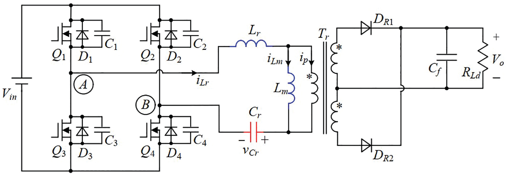
Main topology of LLC full-bridge resonant converter. 23
The frequency fr is defined as the resonance frequency when Lr and Cr resonate. 24 The frequency fr is expressed as follows:

The frequency fm is defined as the resonance frequency when Lr, Lm, and Cr resonated. The frequency fm is expressed as follows:

Frequency conversion mode means that the resonant power converter was controlled by changing the frequency of the switch. The switching frequency was controlled by setting the pulse-width modulation (PWM). It was ensured that the switching tube pulses on the same bridge arm were complementary when switches Q1 and Q4 were turned on and Q2 and Q3 were off. 25
The equivalent circuit of the full-bridge LLC resonant converter is shown in Figure 2. 26 The LLC resonant power converter has two resonant frequencies according to equations (1) and (2). The frequency fr is the maximum resonance frequency. The frequency fm is the minimum resonance frequency. Only Lr and Cr resonate at the maximum resonance frequency point, which is equivalent to a short circuit of the resonance network composed of them. The equivalent circuit is shown in Figure 3(a). Lm, Lr, and Cr resonate together at the minimum resonance frequency point, which is equivalent to the short circuit of the resonance network. No current flows through the secondary side of the transformer at this time. The equivalent circuit is shown in Figure 3(b).

Equivalent circuit of LLC resonant power converter. 26
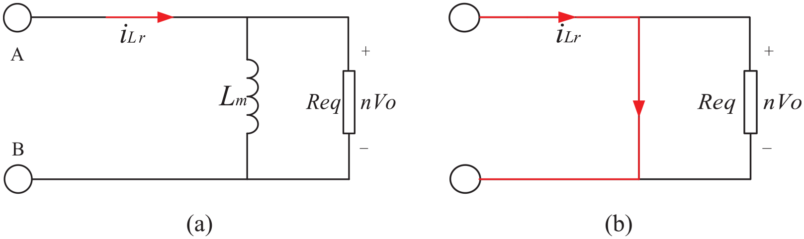
Resonant equivalent circuit of Lm, Lr, and Cr: (a) resonant equivalent circuit composed of Lm and Lr and (b) resonant equivalent circuit composed of Lm, Lr, and Cr.
The working frequency is defined as fk to study the working characteristics at different frequencies. The working frequency and resonance frequency are studied based on the following three cases.
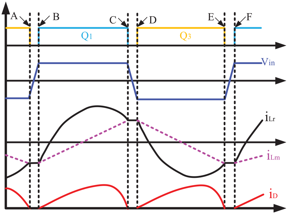
(1) The operating waveform of the resonant converter when fk > fr is shown in Figure 4. 27 The light blue waveform is the driving waveform of switches Q1 and Q4. The yellow waveform is the driving waveform of switches Q2 and Q3. The blue waveform is the voltage waveform at both ends of AB in Figure 2. The black waveform is a resonance current waveform, the purple waveform is the excitation current waveform, and the red waveform is the output current waveform. Point A represents the time when switches Q2 and Q3 are turned off. The voltages at both ends of AB in Figure 2 change from negative to positive from point A to point B. The resonance current decreases and the excitation current increases linearly. The output current decreases to zero at point B. Point B represents the time when switches Q1 and Q4 are turned on. The voltages at both ends of AB in Figure 2 remain unchanged from point B to point C. The resonant current decreases first to zero and then increases in the reverse direction. The excitation current decreases linearly to zero and then increases linearly in the reverse direction. The output current increases first and then decreases. Points D, E, and F are similar to the points in the previous time analysis. The secondary side diode always has a current flowing when the switching frequency is higher than the maximum resonance frequency. The excitation inductance does not participate in the resonance. The voltages at both ends of the excitation inductance are clamped and determined by the turn ratio of the transformer. The voltage does not change. The switches of the super front bridge and the lagging bridge are alternately turned on. A change in the voltage direction of the transformer causes one diode to turn off and the other diode to turn on. There is a problem with reverse recovery when the diode is turned off. At this time, the diode is hard turned off.
(2) The operating waveform of the resonant converter when fk = fr is shown in Figure 5. 28 Points A to F are critical time points. The analyses of the switch drive, voltage of AB in Figure 2, excitation current, resonance current, and output current were similar to those for Figure 4. The results in Figure 5 are different from those in Figure 4 in time periods A to B and C to D. At this time, the excitation current in Figure 5 is equal to the resonance current. The diode has no current when resonance occurs, and the diode could realize ZCS.
(3) The operating waveform of the resonant converter when fm < fk < fr is shown in Figure 6. 29 Points A to H are critical time points. The analyses of the switch drive, voltage of AB in Figure 2, excitation current, resonance current, and output current are similar to those in Figure 5. Figure 6 is different from Figure 5 in time periods C to D and F to G. The resonance currents from point C to point D and from point F to point G are equal to the excitation current in Figure 6. At this time, it is in the resonance state. The ZVS and ZCS could be realized. This operating frequency is beneficial to reduce loss.

Frequency fk > fr operating waveform.
Frequency fk = fr operating waveform.
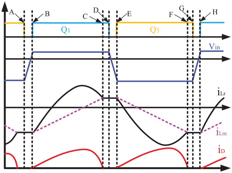
Frequency fm < fk < fr operating waveform.
In summary, both ZVS and ZCS could reduce losses based on the comparison of the switching frequency operating ranges. The switching frequency between the maximum resonance point and the minimum resonance point could realize ZVS and ZCS. To improve the efficiency of the power converter, the operating frequency of the switch should be between the switching frequencies of the maximum resonance point and the minimum resonance point.
To simplify the analysis, an equivalent circuit model was established, as shown in Figure 2. The input impedance was expressed as follows:

The AC voltage gain of the converter is expressed as follows:

M is defined as the voltage gain of the power converter. The expression is as follows:

According to equation (4), the voltage gain of the power converter is expressed as follows:

Because the expression of the voltage gain is complex, normalization is performed to reduce the difficulty of analysis. γ is defined as the ratio of the excitation inductance Lm and the resonance inductance Lr. The quality factor Q is defined as the ratio of the resonance impedance to the output resistance. The normalized frequency fn is defined as the ratio of the operating frequency to the resonance frequency. The expressions for γ, Q, and fn are as follows:

where Zr denotes the resonance impedance.
The following equation is obtained from equations (6) and (7):

Thus, the gain curve of the LLC resonant converter is only related to the parameters fn, γ, and Q.
To study the gain characteristics, the effect of γ on the gain was investigated for different quality factor Q values. The quality factor Q was set to 0.5, 1, and 1.5, and γ was set to 2, 3, 4, 5, 6, 7, and 8. The voltage gain curves were plotted in MATLAB and are shown in Figure 7. The curve was highest when the value of Q was 1 and the value of γ was 2, as shown in Figure 7(a). The curve of the gain increased with the increase in the normalized frequency when the normalized frequency was less than 1 at the same γ. The gain curve decreased with the increase in the normalized frequency when the normalized frequency was greater than 1 at the same γ. The gain curve decreased as the value of γ increased when the normalized frequency was greater than 1 at the same normalized frequency. For all values of γ, the curves all pass through the point (1, 1) in Figure 7(a). The gain increased overall when the quality factor Q value was fixed at 0.5, as shown by comparing Figure 7(b) with 7(a). For all values of γ, the curves also all pass through the point (1, 1) in Figure 7(b). This indicated that the overall gain increased when the quality factor Q was less than 1. The gain decreased overall when the quality factor Q was fixed at 1.5, as shown by comparing Figure 7(c) with 7(a). For all values of γ, the curves also all passed through the point (1, 1) in Figure 7(c).

Voltage gain curves for different quality factors Q: (a) Q = 1, (b) Q = 0.5, and (c) Q = 1.5.
Similarly, the gain was studied for different values of Q and γ. The values of γ were set to 0.5, 1, and 10, and the values of Q were set to 0.4, 0.5, 0.6, 0.8, and 1. The voltage gain curves were plotted in MATLAB and are shown in Figure 8. The voltage gain increased first and then decreased with the normalized frequency for the same value of Q when the value of γ was 1, as shown in Figure 8(a). The gain decreased with the increase in the quality factor Q at the same normalized frequency. The variation trend in Figure 8(b) was similar to that in Figure 8(a) when the value of γ was 0.5. The overall gain increased. This showed that the voltage gain increased at the same normalized frequency when the value of γ was less than 1. The variation trend of Figure 8(c) was similar to those of Figure 8(a) and (b) when the value of γ was 10. The overall gain was reduced. Regardless of the value of the quality factor Q, the gain curve passed through the point (1, 1). This showed that the voltage gain decreased at the same normalized frequency when the value of γ was greater than 1.
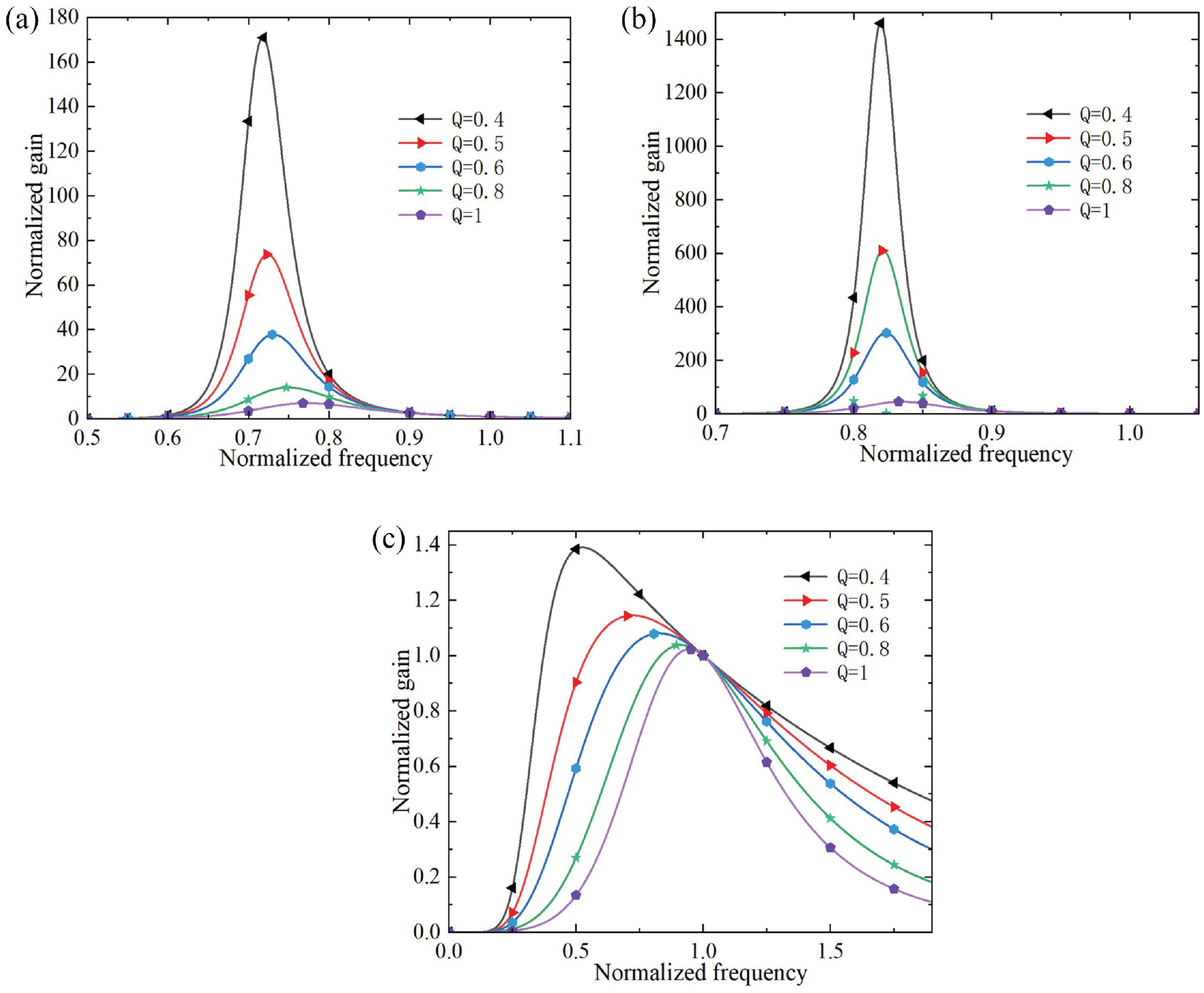
Voltage gain curves for different values of γ: (a) γ = 1, (b) γ = 0.5, and (c) γ = 10.
The input voltage regulation ability became poor due to the decrease in the peak value of the gain curve. If the power converter requires a wide range of input voltages, the value of Q should be less than 1. The operating frequency range increased with the increase in γ. The increase in γ would increase the design difficulty. The selected value of γ should be greater than 1 but not too large. Frequency conversion mode is applicable to non-light-load conditions. Therefore, considering the design difficulty of the compensation network and power efficiency, reasonable values of γ and Q should be selected.
Frequency conversion mode means that the corresponding switching phases of the super front bridge and the lag bridge are the same. The influence of the working frequency on the power converter was studied. 30 To study the phase shift mode, the influence of the switches on the super front bridge and the lag bridge with different phases on the resonant converter were examined. The characteristic of this mode is that the switches of the super front bridge and the lagging bridge are not turned on or off at the same time. When the switching phase on the super front bridge and the lagging bridge is 0, it means that they are in the same phase. At this time, it is in frequency conversion mode.
The phase shift operation waveform is shown in Figure 9. 31 Point A is the turn-off time of switch Q3, and point B is the turn-on time of switch Q1. The voltage waveform at both ends of AB in Figure 2 decreased to zero from time point A to time point B. The excitation current increased linearly, the resonance current decreased, and the output current decreased. Switches Q1 and Q2 were on, and the excitation current at time point C was equal to the resonant current. The voltages at both ends of AB in Figure 2 were zero and unchanged from time point B to time point C. The output current decreased to zero at point C. Point D was the moment when switch Q2 was turned off. The voltages at both ends of AB in Figure 2 were also zero and unchanged from time point C to time point D. The excitation current, resonance current, and output current were the same in the period from point B to point D. The point E was the conduction time of switch Q4. The voltages at both ends of AB in Figure 2 increased from zero. The excitation current, resonance current, and output current also remained unchanged. Point F was the turn-off time of switch Q4. The voltages at both ends of AB in Figure 2 remained unchanged from time point E to time point F. The excitation current decreased linearly to zero and then increased. The resonance current decreased to zero first, then increased in the reverse direction, and then decreased. The output current increased first and then decreased. Time points G to M were similar to the time points in the previous time analysis. The resonance could reduce the loss. The harmonic component of the phase-shifting mode increased. To avoid the influence of the fundamental component on the error, the time-domain analysis method was used. The time-domain analysis method was used to avoid the large errors caused by using the fundamental wave component.

Phase shift working waveform.
The circuit expressions in the period of switching from off to on between points C and D are as follows:

where Im denotes the maximum value of the excitation current.
Similarly, the corresponding equations of other periods are listed. To facilitate the analysis using the time-domain analysis method, the equations are standardized below. Assuming that the switch is in an ideal state, the on and off times of the switch are disregarded. The resonance phase angle is defined as follows:

where D denotes the duty cycle. It is expressed by the ratio of the on time and half cycle for the switches of the super front and lag bridges.
The expressions at different times in the phase shift mode are normalized as follows:


It can be seen from the phase-shift operation waveform diagram in Figure 9 that the voltage and current waveforms in the resonant circuit were symmetric within one cycle. The boundary conditions of the inductance current and capacitor voltage of the resonant network are expressed as follows:

It can be seen from the phase shifting operation waveform in Figure 9 that the excitation current changed linearly and the integral was zero when the excitation inductance did not participate in the resonance. In this period, the resonance inductance and the capacitor resonated, which was equivalent to a short circuit. The current of the resonance inductance changed nonlinearly, and the current change was the charge change of the resonance capacitor. The current expression is as follows:

The equation obtained by collation is as follows:

The following three equations were obtained by combining equations (11) to (16):

The number of parameters in the above formula was greater than the number of equations, so the above equations were implicit functional equations. The parameters are defined as follows:

where
Equation (17) is still an implicit function. To study the gain characteristics in phase shift mode, Ln was selected as 4, and fN was selected as 1. To study the effect of the quality factor Q on the gain, the values of Q were set to 0.05, 0.1, 0.5, 1, 2, and 3. The gain, duty cycle, and quality factor curves are drawn in Figure 10. The curve was at the top when Q was 0.05, and the curve was at the bottom when Q was 3. The gain increased with the increase in Q for the same duty cycle. The gain increased with the increase in the duty cycle for the same value of Q.

Phase shift mode gain curve.
The output voltage in the phase shift mode is determined by the duty cycle. 32 The resonant converter could achieve a boost when M was greater than 1, it was at the resonant frequency point when M was equal to 1, and it could realize step-down when M was less than 1. The phase shift mode is generally suitable for loads with small variation ranges.
Soft switch control strategy
Based on the analysis of the two control modes above, the phase shift mode is generally suitable for working conditions with small load changes, and the frequency conversion mode is generally used for non-light loads. To ensure that the DC-DC resonant power converter could operate in the full load range, a fuzzy adaptive PID frequency-conversion phase-shift control strategy is proposed. The workflow of the soft switch control strategy is shown in Figure 11.

Workflow of the soft switch control strategy.
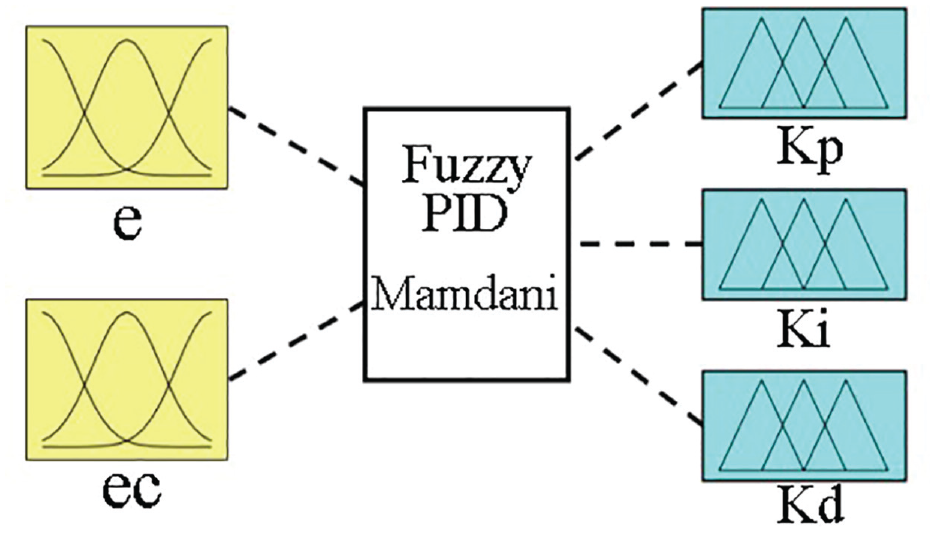
PID control has the advantages of simplicity, high robustness, and high reliability. It is difficult to determine a mathematical model for nonlinear and time-varying systems. Traditional PID control faces problems such as complex parameter tuning, unsatisfactory results, and poor adaptability. Fuzzy control and traditional PID are combined in this paper. Fuzzy reasoning is used to automatically achieve the optimal tuning of the PID parameters to meet the needs of DC-DC power converters. The structural block diagram of the fuzzy PID controller is shown in Figure 12.

Structure of fuzzy proportional–integral–derivative (PID) controller.
The fuzzy adaptive PID was designed using MATLAB. The fuzzy adaptive system is shown in Figure 13. The system had two inputs and three outputs. The difference between the actual voltage and the ideal voltage was defined as e. The error rate of change was defined as ec.
Fuzzy adaptive system.
The fuzzy subset of voltage differences and error change rates was defined as {NB,NM,NS,ZO,PS,PM,PB}. The fuzzy universe was [−27.5, 27.5]. Gaussian functions were used as membership functions. Fuzzy subsets Kp, Ki, and Kd were defined as {NB,NM,NS,ZO,PS,PM,PB}. The precision and response time of the control system are directly impacted by Kp value. A higher Kp compromises the stability of the system, while a lower Kp can slow down response times. In order to make sure that the output voltage is within a particular range, the response time and stability are taken into account. The variation of Kp was set to be in the range of [−0.3, 0.3] to improve the reaction speed based on experience. 33 Triangular membership functions were selected for Kp, Ki, and Kd to improve the sensitivity and facilitate the adjustment. The input and output membership functions are shown in Figure 14.

Input and output membership function: (a) membership functions of input, (b) membership functions of Ki and Kp, and (c) membership functions of Kd.
The core of fuzzy reasoning is to formulate fuzzy control rules based on experience and experimental data to meet the self-adaptive requirements. When e = NB and ec = NB, taking into account the response speed and error, the outputs are defined as Kp = PB, Ki = NB, and Kd = NB. When e and ec increase, the values of Kp = PB and Ki = NB increase. When e = ZO and ec = ZO, to reduce the influence of the differential gain in consideration of system overshoot, the outputs are defined as Kp = ZO, Ki = ZO, and Kd = ZO. The value of Kd is required to increase when e and ec increase. When the overshoot is large, if e = PB and ec = PB, then Kp = NB, Ki = PB, and Kd = PB, and when e and ec increase, the values of Kp and Ki decrease. The fuzzy rules for designing the fuzzy controller are shown in Table 2.
Fuzzy rule table of fuzzy controller.

The output surfaces of the fuzzy adaptive Kp, Ki, and Kd are shown in Figure 15 according to the formulated fuzzy rules. The variation trends of the three surfaces followed a gradient distribution. This indicated that the defined adaptive adjustment requirements were met. 34 The working flow of the fuzzy adaptive PID is shown in Figure 16. The sampled values determined e and ec. The input variables e and ec were blurred. ΔKp, ΔKi, and ΔKd were determined from the fuzzy rule table. The real-time values of Kp, Ki, and Kd were calculated, and the fuzzy adaptive PID adjustment was completed.

Fuzzy adaptive output surface.

Working flow of fuzzy adaptive PID controller.
To verify the formulated fuzzy adaptive PID controller performance, the transfer function is defined as G(s) = (s + 1)/(s2 + s + 1). A simulation model was built based on the previous scholar’s study. 35 MATLAB/SIMULINK was used to build fuzzy adaptive and traditional PID simulation models, and the simulation results are shown in Figure 17. It can be seen from Figure 17(b) that the peak value of the traditional PID control method was at point A. The peak value was 1.3 at 3.3 s. The output of the fuzzy adaptive PID control was the highest at point B. The highest value was 1.03 at 4.0 s. It was found that although the traditional PID control had a fast rising speed, the fuzzy adaptive PID control could quickly stabilize at 1 based on the simulation results of the two control modes. This showed that the fuzzy adaptive strategy could stabilize the output voltage effectively.
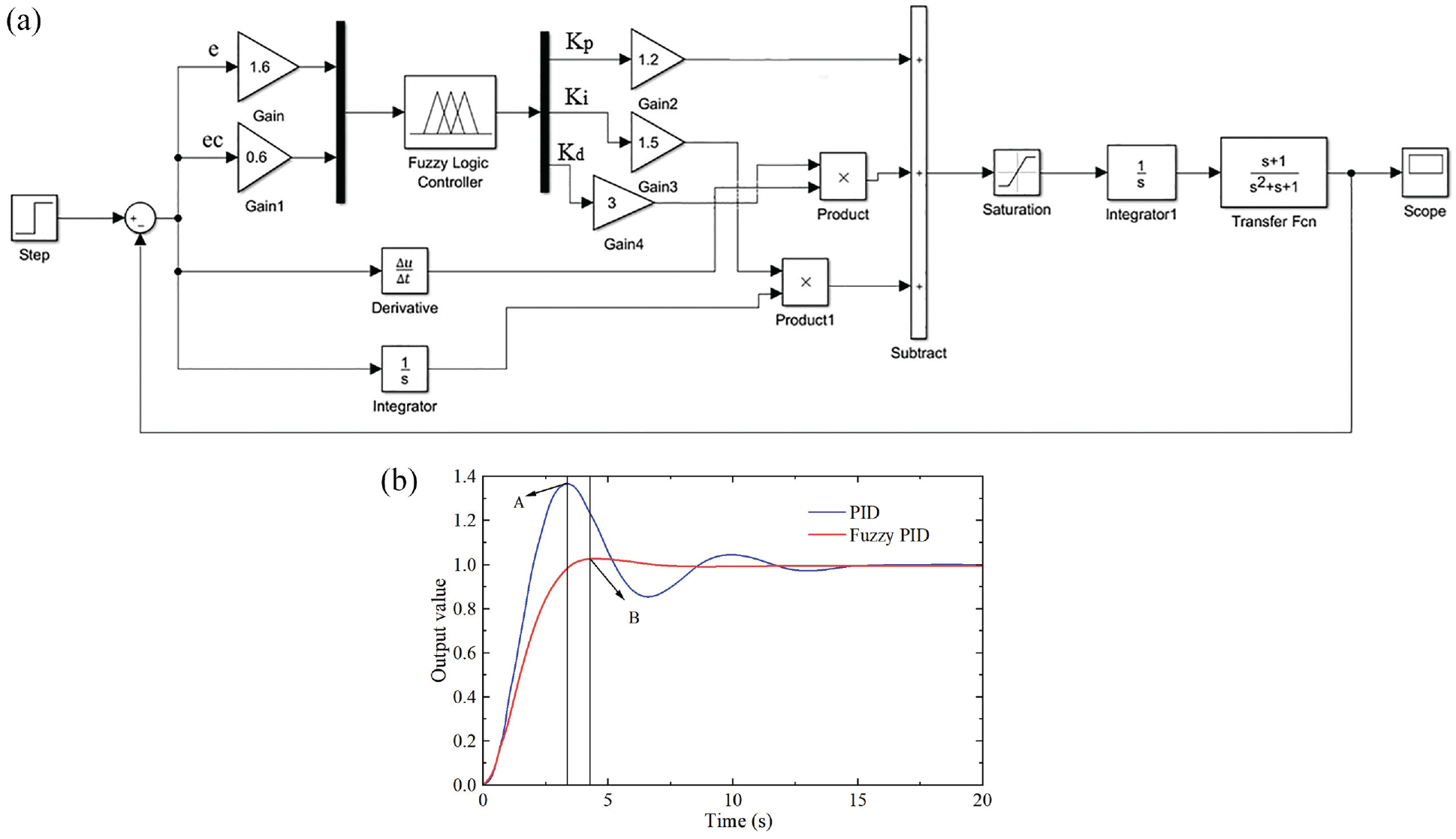
Fuzzy adaptive PID and traditional PID simulation: (a) fuzzy adaptive PID and traditional PID simulation models and (b) simulation results.
Transformer design
The voltage range of the power battery of the pure electric vehicle was 380–700 V, and the required voltage of the electric appliances was 27.5 V in the vehicle. The design of the planar transformer was determined by the parameters of the DC-DC power converter. The design parameters of the DC-DC power converter are shown in Table 3.
Design parameters of plane transformer.

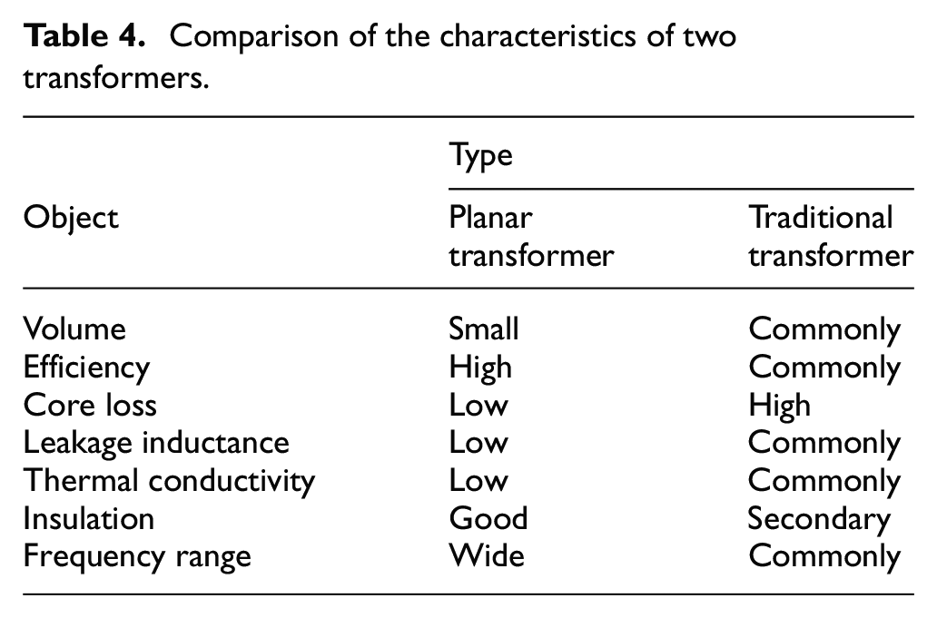
As technology improves, the performances of DC-DC power converters have higher requirements. A transformer is an important device for the voltage regulation of a power converter. Power converters are developing in the direction of small sizes, high powers, and high efficiencies. The comparison of the characteristics of a traditional transformer and a planar transformer is shown in Table 4. The planar transformer had advantages over the traditional transformer. 36 Thus, the planar transformer was selected to design the power converter in this paper.
Comparison of the characteristics of two transformers.
A transformer plays the role of regulating the voltage in a DC-DC power converter, and the design of a transformer is very important. The design process of the planar transformer was similar to that of a traditional transformer. In addition to meeting the design parameters, the designed planar transformer also needed to reflect the advantages of a low loss, small volume, and low cost. 37 The design flow of the planar transformer is shown in Figure 18. The design of the planar transformer mainly involved the selection of the magnetic core, parameter calculation, winding structure, and temperature rise.
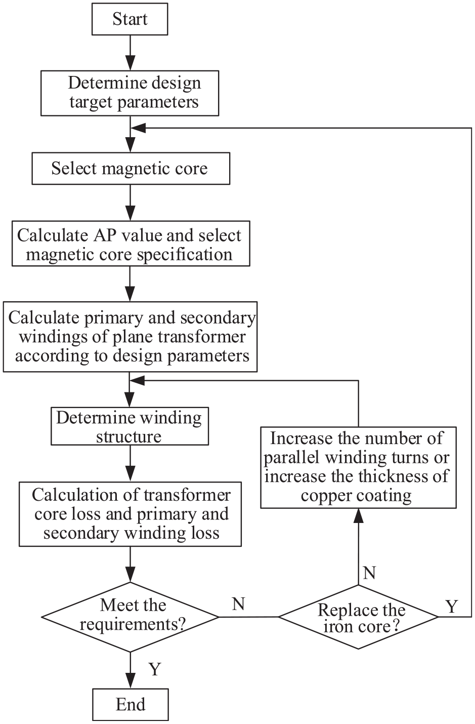
Design process of a plane transformer.
According to the plane transformer parameters of Table 3, the turn ratios of the primary and secondary windings were preliminarily calculated. The maximum duty cycle needed to be determined before calculation. Since the minimum input voltage and the saturation strength of the magnetic core needed to be considered in the calculation, the limit duty ratio was defined as 0.95, namely Dlim = 0.95. The maximum duty ratio was generally taken as 10% of the limit duty ratio in the calculation. The maximum duty ratio was 0.85 in the calculation, namely Dmax = 0.85.
The secondary side rectification network is composed of diodes with a voltage drop of 0.6 V. The secondary output voltage of the transformer is expressed as follows:

where VD represents the diode voltage drop.
The turn ratio of the primary and secondary windings was calculated as follows:

The area product method was used to select the magnetic core of the planar transformer. The expression of the AP method is as follows:

The magnetic core ER120 was selected, and the calculated AP was greater than 18.6. This margin could meet the design requirements.
As shown in the transformer design flowchart in Figure 17, the loss of the planar transformer was calculated after the magnetic core was determined. The transformer loss mainly came from the core loss and the coil loss. The modified Steinmetz equation was used to calculate the core loss in this study. 38 The expression of the core loss is as follows:

To reduce the calculation difficulty, the coil loss PWloss was considered to be equal to the core loss PMSE. The loss expression of the planar transformer is as follows:

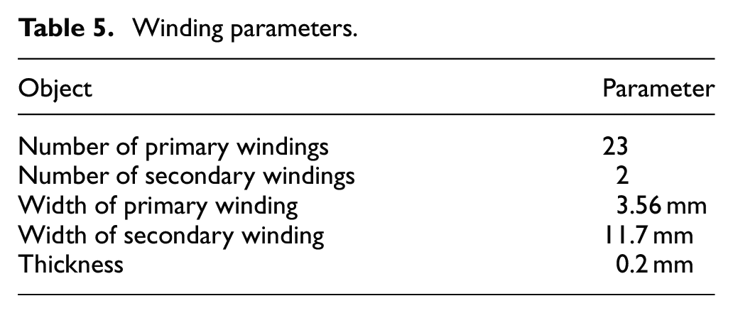
The number of secondary windings was calculated as follows:

The number of windings should be an integer. Thus, the number of turns of the secondary winding was taken to be two, that is, Ns = 2.
The number of turns of the primary winding was calculated from the turn ratio and the number of turns of the secondary winding. The number of primary windings was calculated as follows:

Again, the number of windings should be an integer. Thus, the number of turns of the primary winding was taken as 23, that is, Np = 23.
The expression of the effective current of the primary winding was as follows:

The expression of the effective current of the secondary winding was as follows:

The penetration depth of the winding at 100°C was as follows:

The expression of the cross-sectional area of the primary winding was as follows:

The cross-sectional area of the secondary winding was as follows:

The Copper–Covering expression was as follows:

where N represents the number of turns of a single-layer winding, and S1 represents the minimum distance between the copper coating and the inner and outer columns of the core window.
The resonant power converter operated at a high frequency, and the alternating current in the winding exhibited a skin effect. The skin effect would make the current gather on the winding surface, resulting in uneven current distribution and increased loss. The winding thickness was designed to be within twice the penetration depth to reduce the skin effect in this study. The winding parameters are shown in Table 5.
Winding parameters.
Simulation
Full-bridge LLC circuit simulation
To verify the feasibility of the proposed control strategy, the LLC fuzzy control frequency conversion circuit model was constructed in MATLAB/SIMULINK and is shown in Figure 19. Region A of Figure 19 is a switch network composed of four switches. Region B of Figure 19 is a resonant network composed of inductance and capacitance. Region C of Figure 19 is a rectifier network composed of diodes.

LLC fuzzy control frequency conversion circuit model.
Non-light-load simulations were carried out under frequency conversion mode. The simulation results of the switch, excitation current, resonance current, and output current are shown in Figure 20. The blue waveforms are switches Q1 and Q3 and the red waveforms are switches Q2 and Q4 in Figure 20. This indicated that the switch driving voltage was 15 V. The resonant currents in regions A to H in Figure 20 were equal to the excitation currents, and resonance occurred in these regions. Regions A to H in Figure 20 correspond to regions a to h in Figure 20, respectively. This indicated that no current flowed through the output diode during resonance. ZVS and ZCS could be realized, the loss could be reduced, and the efficiency could be improved. The simulation results were consistent with the theoretical analysis.
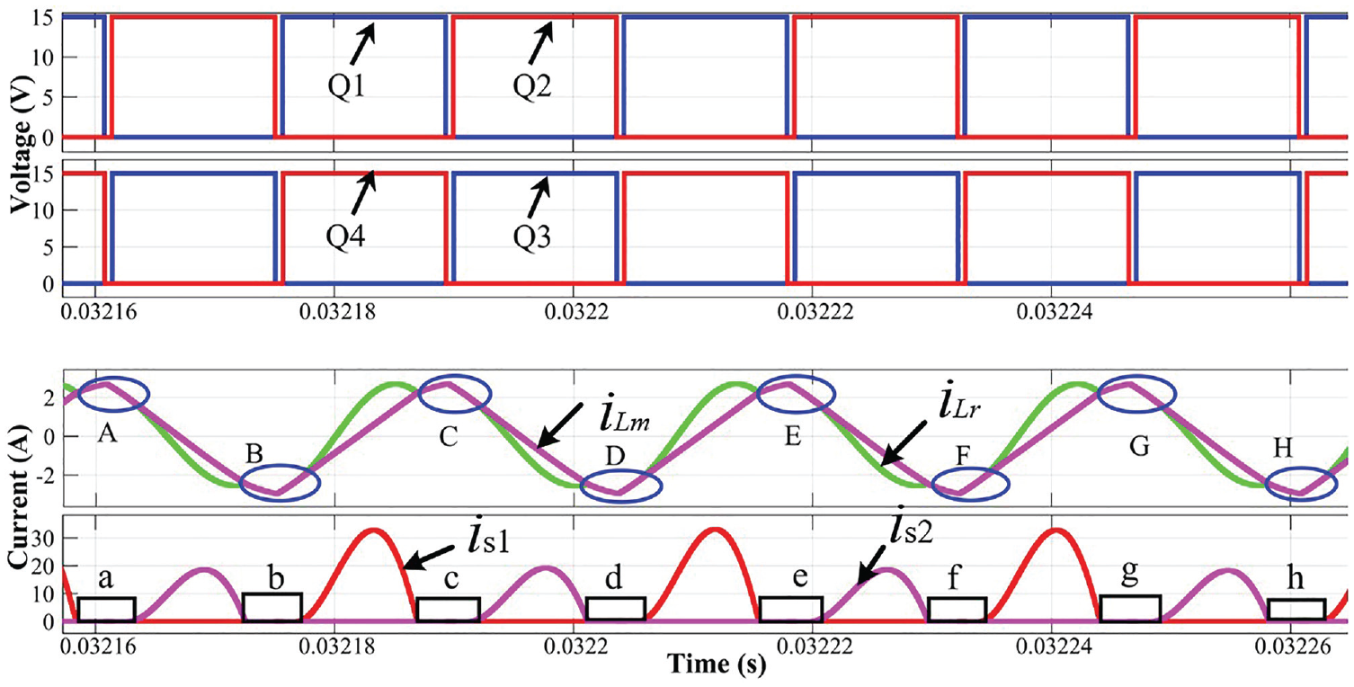
Non-light-load simulation results under frequency conversion mode.
Simulation and optimization of planar transformer
It is known that transformers mainly solve electrical and magnetic problems. The powerful and accurate Ansys Electronics Desktop software was selected to simulate the planar transformer in this paper. 39 The structure of the transformer winding would have an impact on the transformer due to the existence of AC impedance. 40 The uncrossed winding structure and the winding structure of the complete cross are shown in Figure 21. Yellow represents the primary winding, white represents the insulation layer, and blue represents the secondary winding in Figure 21. The two-dimensional diagram of the planar transformer winding was drawn using the ANSYS Electronics Desktop. The winding structure in Figure 21 is a two-dimensional model without chamfers, so the simulation does not require excessive time. The maximum element length is set 1 mm when dividing the grid in order to achieve the best simulation results. Since the model is relatively simple, it does not affect the running speed. The meshes of the two winding structures are shown in Figure 22. The grid shape was set to a triangle. By observing the shape of the unit, it was found that the triangle was approximately equilateral. The grid aspect ratio was close to 1, and the analysis of the grid aspect ratio indicated that the drawn transformer winding grid was of good quality. 41 To determine the AC impedance, the magnetomotive force was simulated by Ansys Electronics Desktop. A structure with a small impedance was selected for the design.
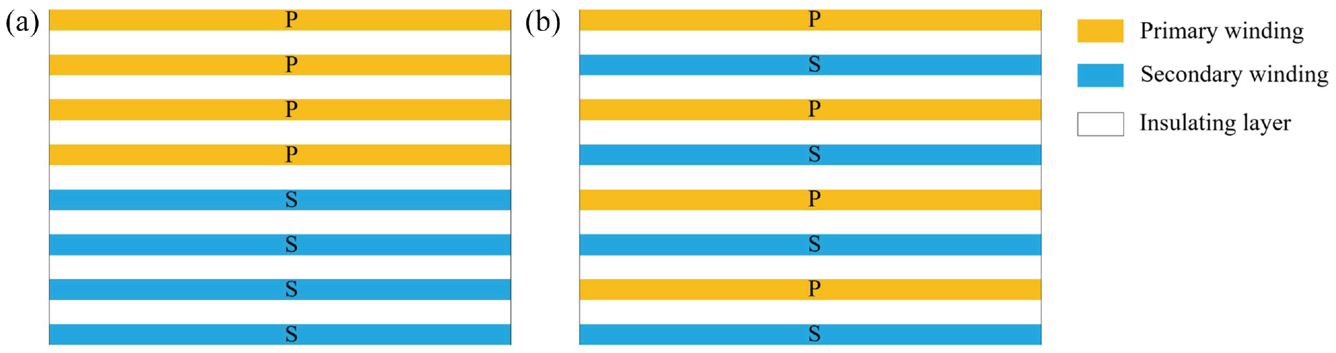
Uncrossed and complete cross winding structure: (a) uncrossed winding structure and (b) complete winding structure.

Two-dimensional model meshes of two kinds of winding structures: (a) uncrossed structural mesh and (b) complete cross structural mesh.
To ensure that the simulation result was realistic, the primary side current was set to 1 A and the secondary side current was set to 12 A based on the turn ratio of the transformer. The working frequency was set to 60 Hz, 35 kHz, 85 kHz, and 135 kHz for the simulation. The current density simulation results are shown in Figure 23. The operating frequencies of 60 Hz, 35 kHz, 85 kHz, and 135 kHz correspond to the black, red, blue, and green curves, respectively, in Figure 23. As can be seen in Figure 23(a), the operating frequency of the 60-Hz current density distribution was uniform. With the increase in the frequency, the current density of the uncrossed structure decreased with the increase in the working frequency. This indicated that the greater the working frequency was, the greater the influence on the planar transformer was. The current density of the complete cross winding structure was small, and the influence on the current density was small as the frequency increased based on the comparison of Figure 23(a) and (b). It is shown that the planar transformer’s complete cross structure had a low AC impedance, and the use of a complete cross structure could reduce the heat generated and improve the efficiency of the planar transformer.

Current density simulation: (a) current density distribution of uncrossed structure and (b) current density distribution of complete cross structure.
The cloud diagram of the simulated current density with an operating frequency of 85 kHz is shown in Figure 24. The distribution range in Figure 24(a) was [−1.929 × 10⁷, 2.9828 × 10⁶], corresponding to a color variation range between blue and red. The distribution range in Figure 24(b) was [−1.5742 × 10⁷, 3.2564 × 10⁶], corresponding to a color variation range between blue and red. The complete cross structure of the planar transformer winding was more evenly distributed based on the comparison of Figure 24(a) and (b).

Cloud diagram of current density distribution: (a) uncrossed structure and (b) complete cross structure.
The simulation results of the magnetic lines of the two windings of the plane transformer at the working frequency of 85 kHz are shown in Figure 25. The density of the magnetic lines represents the distribution of the magnetic field. The range in Figure 25(a) and (b) was [−0.132 × 10⁶, 0], corresponding to a color change range from blue to red. The distribution of the magnetic lines of the two structures was not much different based on the comparison of Figure 25(a) and (b). This showed that the magnetic field distribution of the planar transformer was not affected by the winding structure. The loss simulation structure of the two windings under four different operating frequencies is shown in Table 6. The simulation results showed that the full cross winding structure had less loss at the same working frequency, which was consistent with the previous analysis. The full cross winding structure was more conducive to improving efficiency.

Simulation of magnetic line distribution: (a) uncrossed structure and (b) complete cross structure.
Simulated loss results for two winding structures.

Experiment
Planar transformer
The photograph of the designed full cross plane transformer is shown in Figure 26. The planar transformer was composed of a magnetic core and a winding. The distributions of the planar transformer windings in the drawing board software are shown in Figure 27. Figure 27(a) to (d) show the primary windings of the transformer and Figure 27(e) and 27(f) show the secondary windings of the transformer. This verified the proposed control strategy and tested the characteristics of the DC-DC power converter. An experimental platform for experiments was then constructed.

Photograph of the planar transformer.
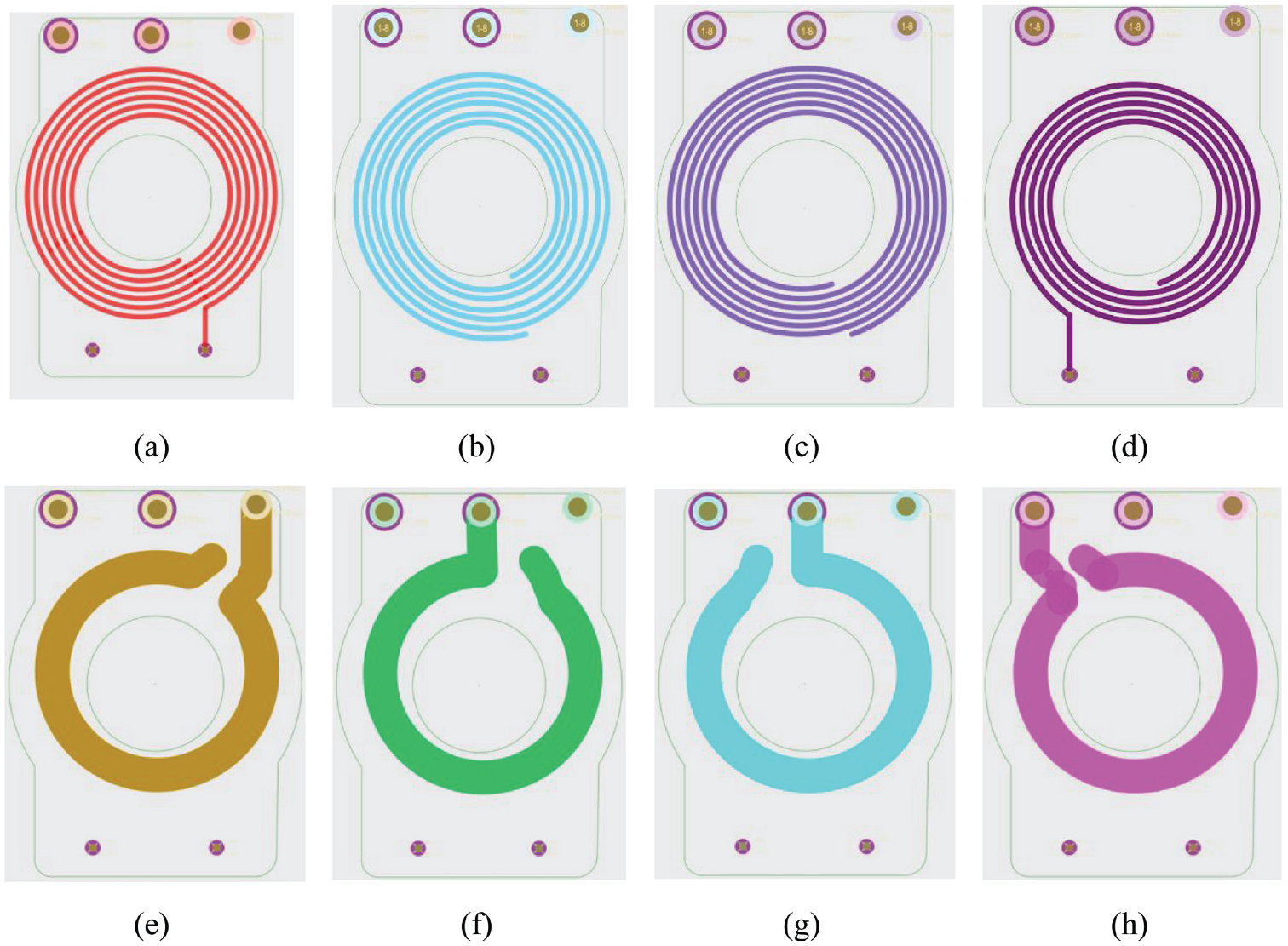
Distribution of the planar transformer windings: (a) primary-side first-layer winding, (b) primary-side second-layer winding, (c) primary-side third-layer winding, (d) primary-side fourth-layer winding, (e) secondary-side first-layer winding, (f) secondary-side second-layer winding, (g) secondary-side third-layer winding, and (h) secondary-side fourth-layer winding.
Experimental platform
According to the input and output characteristics of DC-DC the power converter, the block diagram of the designed experimental platform and the wiring of the main experimental equipment are shown in Figure 28. The high-voltage power supply simulated the power battery of a pure electric vehicle. The computer was used to monitor the status of the DC-DC power converter. The low-voltage power supply served as the auxiliary power supply to drive the switch and control circuit. The oscilloscope could capture the voltage and current waveforms. It could provide a basis for analyzing the characteristics of the power converter. An electronic load instrument was used to simulate the electrical equipment of a pure electric vehicle. A universal meter was mainly used to measure the output voltage to ensure the accuracy of the data collected by the computer. High-voltage relays, low-voltage relays, and timers could be used to test the mechanical characteristics of the DC-DC power converters. The temperature and humidity text chamber were used to simulate the operating environment of the DC-DC power converter.

Diagram of the experimental platform: (a) block diagram of the experimental platform and (b) wiring diagram of the main experimental equipment.
After setting up the test platform, as shown in Figure 28, first, the low-voltage power supply was turned on to supply power to the power converter. At this time, the software of PC could monitor the power converter through controller area network (CAN). Then, the high-voltage power supply was turned on, and at this time, the input end of the power converter was powered on. Finally, the input voltage and load size were set according to the experimental requirements. The main instrumental parameters are shown in Table 7.
Main instrumental parameters.

Power and efficiency experiment
The simulated and experimental power used an input voltage of 540 V. To study the output powers of different loads, the load was varied from 10% to 100%, and the data were recorded. The experimental and simulation results are shown in Figure 29, where the abscissa represents the load, the left ordinate represents the power, and the right ordinate represents the input voltage. The red curve in Figure 29 is the simulated power. When the input voltage was 540 V and the load was full, the power was 3.12 kW. The black curve with triangles was the power in the experiment. The power was 3.03 kW when the load was full. The blue curve in Figure 29 shows that the 540-V input voltage set by the simulation was constant. The black curve with stars in Figure 29 is the power battery voltage of the experiment. The input voltage decreased with increasing load. This was due to the increase in the load to increase the output current, resulting in an increased voltage drop and larger line loss in the experiment. Because the transformer did not produce loss during the simulation, the simulation output power of the converter was slightly higher than the experimental output power. The curve with black squares in Figure 29 is the power curve of the experimental frequency conversion control. Under the condition of a small load, the power curve of the frequency conversion control increased little with the increase in the load. Under non-light load conditions, the power increased as the load increased. However, when the load was full, the power increased slightly. Thus, there was a control mode switching point. It can be seen from Figure 29 that the black triangle’s curve is above the black square’s curve. The output power achieved using the proposed fuzzy adaptive PID strategy was 20.98% higher than that achieved using a single variable frequency control strategy at the switching point. This indicates that the proposed fuzzy adaptive PID frequency conversion phase-shift control strategy has more advantages than the single variable frequency control strategy.

Simulation and experimental results under 540 V input voltage and different loads.
The working efficiency of the DC-DC power converter was tested at normal temperature by using the experimental platform. The high voltage power supply in the experimental platform was set to 400, 450, 540, and 700 V, and the load was increased from 10% to 100%. The output current and output voltage were recorded. The relationship between the experimental load, input voltage, and calculated power is shown in Figure 30. It can be seen from the color change in Figure 30 that when the input voltage was fixed, the output power increased with the increase in the load. The output power was linear with the load, which was consistent with the output power curve in Figure 29. This showed that the designed DC-DC power converter could stabilize the output power. When the set load was a constant value, although the voltage changed, the color of the surface did not change significantly. This showed that the output power under the same load was stable, and the pure electric vehicle power converter could operate normally within the range of the power battery voltage variations. Thus, it met the design objectives.

Relationship between input voltage, load, and output power.
The working efficiency of the DC-DC power converter designed for the experimental pure electric vehicle in the range of the power battery voltage conversion was investigated. The output powers under different input voltages were tested. The input and output powers were calculated according to the input and output voltages and currents of the experiments. The efficiency formula is as follows:

The efficiency was calculated, and the efficiency experimental curves under four different input voltages are shown in Figure 31.The efficiency curves for 540 and 700 V were both above the efficiency curves of 400 and 450 V, indicating that the efficiency was improved with the increase in voltage within the range of the power battery voltage. When the load was less than 30%, the 400 V efficiency curve was below the 450 V efficiency curve, indicating that the efficiency of a small load was low under a small input voltage within the range of the power battery voltage. The efficiency increased with the increase in the voltage. When the load was greater than 30%, the 400 V efficiency curve was above the 450 V efficiency curve, indicating that in the power battery voltage range, the efficiency first increased and then decreased with the increase in the load under small input voltages. By comparing the 540 and 700 V efficiency curves, it was found that the two efficiency curves were similar under small loads, and the 540 V efficiency curve was above the 700 V efficiency curve under heavy loads. This shows that in the voltage range of the pure electric vehicle power battery, the efficiency decreased with the increase in the voltage under high input voltages. As shown in Figure 31, the efficiency of the power converter increased with increasing load. The minimum and maximum efficiency values were 92% and 97.38%, respectively. Furthermore, it can be seen that the efficiency could reach 95% after the switching point. The experimental results were consistent with the design objectives. This showed that the designed 3-kW DC-DC pure electric vehicle power converter had a low loss and high working efficiency, which could reduce the power battery state-of-charge (SOC) loss, thus improving the driving range.
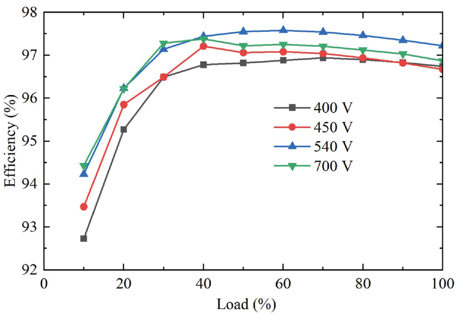
Efficiency test curves under four different input voltages.
The presence of a ripple can lead to the generation of noise in the circuit, which is not conducive to improving the efficiency of the power converter and may even damage the power converter. The voltage probe of the oscilloscope was used to collect voltage ripple at the output end of the LLC resonant power supply (Figure 28). The power converter was placed in a chamber with constant temperature and humidity to test the output voltage ripple under high- (55°C), normal- (25°C), and low-temperature (−40°C) environments. The ripple under three different environments is shown in Figure 32, where the black, blue, and red curves represent the results of voltage ripple tests conducted under the room-, high-, and low-temperature environments. Furthermore, the solid circle and solid hexagon indicate the voltage ripple results of the light and full load tests, respectively. Figure 32 also shows that the voltage ripple of the power converter first increased and then decreased with the input voltage under full load. The voltage ripple of the power converter was relatively stable under no load conditions. The ripple curve of the −40°C environment and 100% load is at the top in Figure 32. The maximum ripple was 472.91 mV. The ripple of different loads under all test environments was less than 500 mV. The designed output voltage error was within 0.5 V.

Voltage ripple of different inputs and loads under three different environments.
Conclusion
This paper presented the optimal design of a 3-kW high-power DC-DC converter for a pure electric vehicle. The main results of this study were as follows.
(1) The full-bridge LLC was selected as the main circuit to meet high-power requirements. To reduce the difficulty of the research, the equivalent circuit was determined, and the circuit characteristics were analyzed.
(2) The working characteristics of the two working modes were analyzed to formulate a soft switching control strategy of the LLC resonant converter so that the switch realized ZVS and the diode realized ZCS. The fuzzy adaptive PID frequency-conversion phase-shift soft-switching control strategy was proposed to reduce losses and improve output voltage stability.
(3) According to the characteristics of pure electric vehicle power batteries and electronic equipment, a fuzzy controller was designed to output a stable voltage.
(4) A complete cross plane transformer was designed. The running simulation software found that the advantages of the designed planar transformer were more significant with the increase in the working frequency.
(5) To verify the feasibility of the strategy control strategy, a MATLAB/SIMULINK circuit model was constructed. The operating waveform was consistent with the theory, which showed the feasibility of the proposed strategy.
(6) To further verify the simulation results and the efficiency of the DC-DC power converter, an experimental platform was built. The experimental results were similar to the simulation results. The power of the fuzzy adaptive PID frequency conversion phase-shift control was higher than that of frequency conversion control. The minimum and maximum efficiency values were 92% and 97.38%, respectively. The proposed control strategy and transformer optimization method could provide a reference for improving the efficiency of power converters and the driving ranges of pure electric vehicles.
Footnotes
Handling Editor: Chenhui Liang
Declaration of conflicting interests
The author(s) declared no potential conflicts of interest with respect to the research, authorship, and/or publication of this article.
Funding
The author(s) disclosed receipt of the following financial support for the research, authorship, and/or publication of this article: This entire study was funded by the Natural Science Foundation of Fujian Province (grant number 2020J01270) and the Fujian Industrial Technology Development and Application Project (grant number 2021I0024).
Data availability
The data used to support the findings of this study are available from the corresponding author upon request.