
Abstract
A wide variety of AC/DC power converter topologies have been developed in order to improve the system efficiency, input power factor and system redundancy for stationary battery energy storage systems. Due to the nature of high-power batteries, there is a big voltage difference between battery terminals from the end of discharge to the high charge value. To prevent unregulated battery voltages from harming the system loads, several techniques are used in the industry. A well-known old technique named as diode dropper is simple but suffers from low efficiency. Using a DC-DC converter is more advantageous, although it increases the cost. In this paper, the use of partial power processing converters which attract interest these days has been proposed as an alternative. The proposed full bridge/push-pull series connected partial power converter has a slight modification compared to the classical one presented in the literature. A system with 22 kW power rating was designed and tested. In order to compare the results, a two-switch buck-boost converter was also designed and tested for the same conditions. The results show that the proposed converter is superior to both the two-switch buck-boost converter and other topologies in terms of efficiency and response speed. Efficiencies of 97%–99% have been attained with the proposed converter.
Introduction
Battery energy storage system (BESS) has become very widespread in the last decade. Although lithium-based batteries are preferred in many applications such as portable devices and electric vehicles, lead-acid batteries and Ni-Cd batteries are still preferred in several applications in industry such as power plants, uninterruptable power supplies, SCADA-monitoring systems, DC substation systems, electrical vehicles, aircrafts and telecom applications. Existence of batteries in all these applications requires the use of battery chargers with the desired characteristics depending on the battery type.
Due to the nature of the charge–discharge characteristics of batteries there is a large variation of voltage at the battery terminals in a complete charge discharge period.1–7 To protect DC loads from this unregulated voltage, many special designs are implemented such as diode droppers, DC-DC converters or float cum boost chargers.8,9
Diode droppers provide a simple solution at the cost of reduced efficiency. A natural choice then is to use a DC/DC converter to regulate the voltage. However, classical converters process the full load power, and they may have high power losses. Processing only part of the rated power instead of the full power supplied to the load has been proposed to improve the performance of converters.10,11 Partial power converters (PPCs) using this concept have been proposed for use with photovoltaic (PV) systems.12–16 Among different approaches, full bridge push pull series connected PPC (FB/PP S-PPC) is claimed to be the most efficient solution to improve the overall efficiency of the DC/DC stage applied to PV systems. 17 S-PPC acts like a voltage regulator; its processed energy is related to the regulated voltage (ΔV). The smaller the regulated voltage, the lower the active power processed by the converter in relation to the output power of the converter. 18
Recently, some studies comparing the step up/down partial power converter and the step-up partial power converter have been reported. Two 750 W prototypes, one full-bridge series partial-power converter (FB S-PPC), and one full-bridge push–pull series partial-power converter (FB/PP S-PPC) were implemented in Zientarski et al. 17 The study shows that FB/PP S-PPC reduces both active and non-active power losses. In Zientarski et al., 18 three 750-W prototypes; one full-bridge phase-shifted series partial-power converter (FB/PS S-PPC), one fly-back S-PPC, and one full-power converter (conventional boost) were compared, and the results show that the FB/PS S-PPC topology achieves the highest efficiency in DC-DC conversion, while the fly-back topology does not behave like a partial power processing converter as expected. An eight-switch buck-boost regulator (ESBBR) topology was proposed as a bus voltage regulator providing ±50% voltage regulation range, bus switching, and overload limiting, operating above 98% efficiency. 19
So far only low-power converters with partial processing have been presented in literature. This paper aims to show that the concept can be used in higher power applications too. Therefore, a FB/PP S-PPC 22 kW (220 V, 100 A) DC/DC converter was designed for a BESS application. Also, a two-switch buck-boost converter (TSBBC), which has the capability of regulating the voltage against voltage drops and rises, was designed for the same application. Both converters were built and tested at the same conditions.
The remaining of this paper has been organized as follows: In section “Charge–discharge characteristics of Lead-acid and Ni-Cd batteries,” some information is given about Lead-acid and Ni-Cd batteries, and BES systems. Operations of the TSBBC and proposed converter are described in sections “TSBBC” and “FB/PP series partial power converters and the proposed topology” respectively. The design processes of the two converters are given in section “Design of FB/PP S-PPC and TSBBC topologies.” Experimental results and comparisons of two converter are given in section “Experimental results and comparisons.”
Charge–discharge characteristicsof lead-acid and Ni-Cd batteries
Valve-regulated lead acid (VRLA) batteries have been used in industry for a long time. They have long life-cycles, maintenance free properties and high-power densities. Their discharge and charge characteristics are given in Figures 1 and 2, respectively.
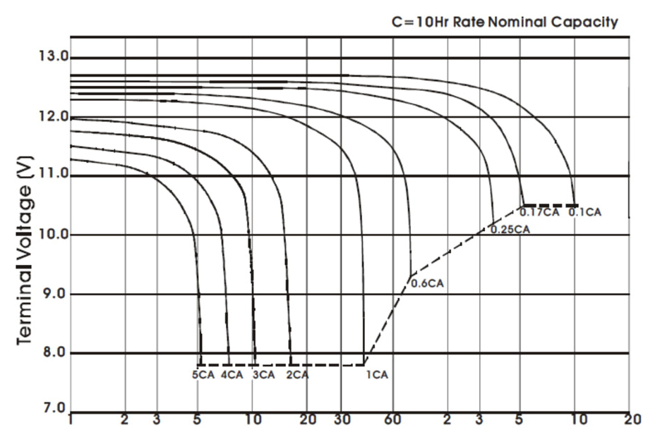
VRLA battery discharge characteristic.
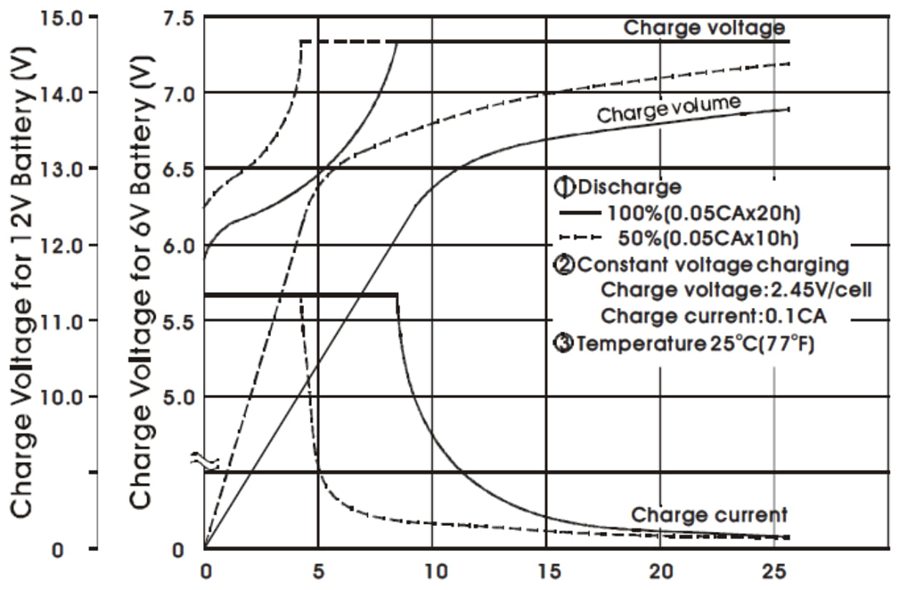
VRLA battery charge characteristic.
Ni-Cd batteries are widely used in the industry and are one of the most reliable systems that can be found in the market. They are often the only reasonable choice when operating under extreme environmental conditions, especially in high temperatures.
Industrial application batteries are used as series and parallel battery packs or cells. The 24 V, 48 V, 110 V and 220 V applications are very common in industry.
A 220-V lead-acid battery storage system can be setup with 18-pack series connected 12 V battery cells or 96-pack series connected 2 V battery cells. As seen from the characteristics given in Figures 1 and 2, for the VRLA batteries the end of discharge value is 10 V, standby charge value is 13.6 V, and overcharge value is 14.5 V.1–3,6 For a 220 V battery bank, the terminal voltage varies between 180 V and 261 V in various charge–discharge conditions.
Likewise, a 220 V Ni-Cd battery storage system can be setup with 180 pack series connected 1.2 V battery cells. It can be seen from literature that, the end of discharge value is 1.0 V, the standby charge value is 1.35 V, and the over-charge value is 1.45 V.4,5,7 For a 220 V battery bank, the terminal voltage varies between 180 V and 261 V in various charge–discharge conditions.
Figure 3 shows a typical connection diagram in a BESS connected directly to a DC load. The voltage variation across the battery bank may be as large as ±20%. Compared to the 220 V nominal bus voltage, this could be unacceptable, and may be dangerous for some critical DC loads.
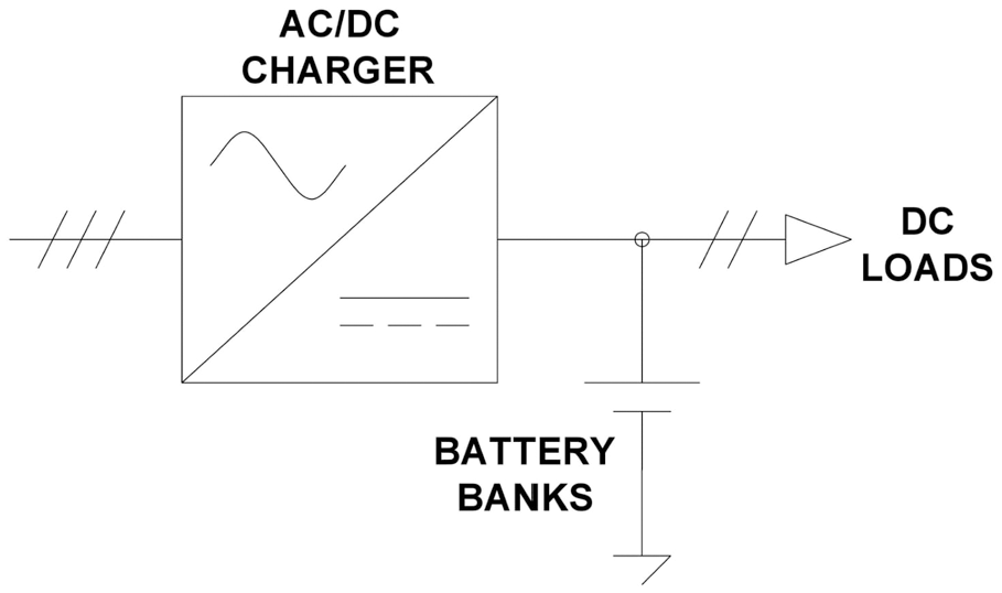
Conventional battery charger with BESS directly connected to DC load bus.
AC/DC battery charger companies offer basic solutions to protect the critical loads from higher value of DC bus voltages.8,9 One solution is basic, a very old solution that uses a diode dropper with a contactor. Figure 4 shows an example application of three-stage diode dropper method between the battery bank and the DC load.
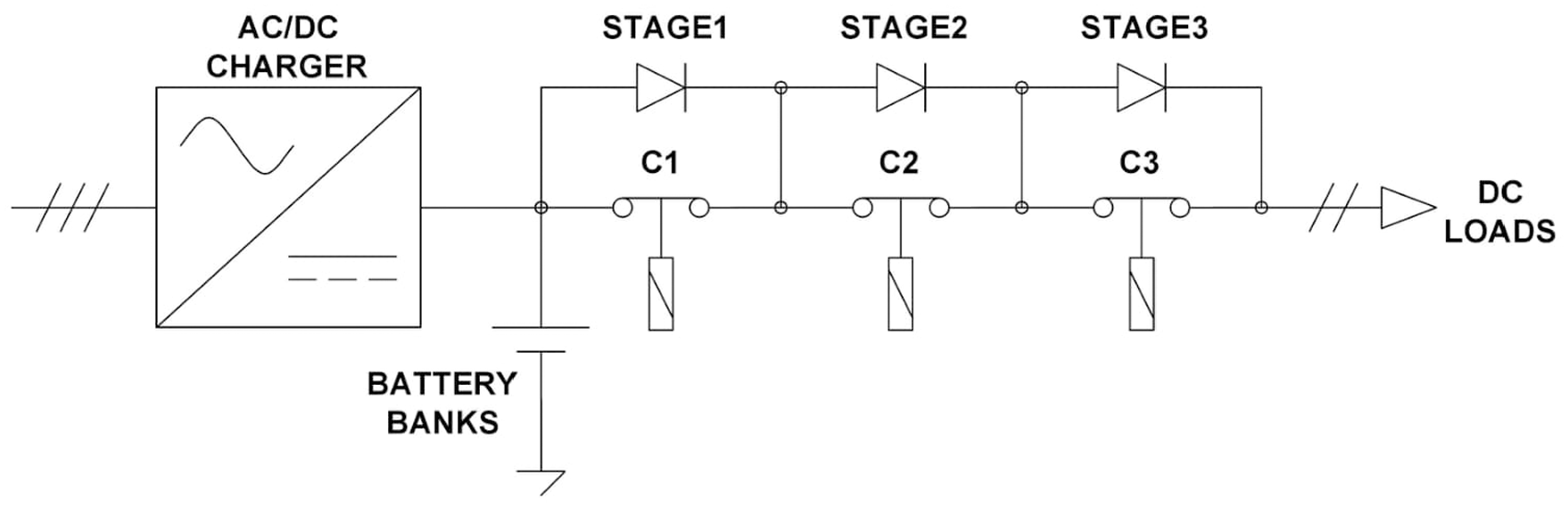
Battery charger with three stage dropper between BESS and DC load bus.
A control and feedback mechanism supplies a healthier voltage (220 ± 5%V) to the loads during charge period, but the control is slow and not perfect because of the mechanical contactor. The dropper has low efficiency and needs heatsink and cooling fan mechanism. It may have a power loss of as much as 15%, reducing the overall efficiency below 85%, ignoring all other losses. If the AC/DC converter efficiency is 90%, the overall efficiency may be around 76%. During the discharge of the battery bank, droppers may be short circuited with the contactor to make the overall efficiency equal to the charger efficiency. However, in this case, the DC voltage becomes unregulated and drops from 220 to 180 V. Another option is to use the float cum boost charger method, utilizing a contactor and a reverse diode between different battery stages with two chargers as shown in Figure 5.
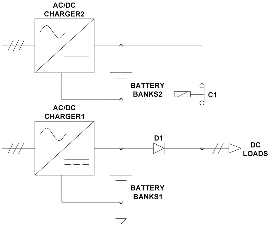
BESS application with float cum boost chargers.
The application seen in Figure 5 is for a 220-V battery storage system design with Ni-Cd battery cells. Battery bank1 (BB1) is set up with 165 series cells (
A monitor and control circuit drives the contactor mechanism to supply a healthier voltage (220 ± 9% V) to loads during the charge period. In the discharge period, DC load voltage is between 224 and 180 V like it is in the dropper diode mechanism. This method is more efficient because there is no power loss equipment in series except only one diode, but the voltage regulation is not good.
TSBBC
Utilizing a DC/DC converter to regulate the voltage as seen in Figure 6 is more advantageous than using the two methods described in the previous section due to higher efficiency and better dynamic response of the former. The converter should be able to step up or down the voltage. Conventional buck-boost converter cannot be applicable because of its reverse polarity between input and output terminals. To overcome the polarity problem, a topology named TSBBC in Chen et al. 20 can be applicable.
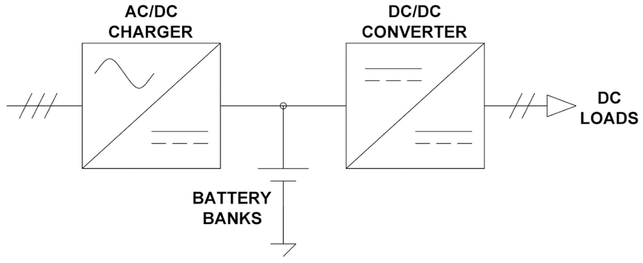
BESS application with DC-DC converter between DC bus and DC loads.
Figure 7 shows the two-switch buck-boost (TSBB) topology which includes two switches, two diodes, one inductor and two capacitors. During the buck mode operation, Q1 is switched on and off and, Q2 is kept off. During the boost mode operation Q2 is switched on and off and, Q1is kept on.
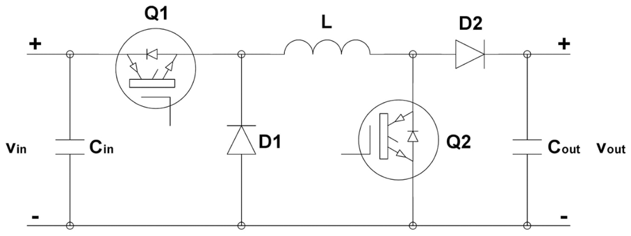
Two-switch buck-boost (TSBB) converter topology.
This topology has many advantages compared to the conventional single switch buck-boost converter for a universal-input power-factor-corrector application. The two-switch converter has the following advantages: lower inductor conduction losses (50%), lower inductor volt-second area (72% of the boost converter) with about the same switch conduction losses and voltage stresses. 20
Improved topologies of TSBB converter were presented in Moon et al.21,22 which claim to have lower conduction losses and switching losses. However, they also have the component stress problem and floating output connection due to the switches on both sides of the output capacitor. Therefore, the TSBBC topology described in will be used in the remaining of this paper for comparison. 20
Equations (1)–(9) define the basic behavior of TSBBC. In these equations


The minimum capacitance and inductance values for the boost mode operation are defined as follows


Similarly, the minimum capacitance and inductance values for the buck mode operation are defined as follows


The worst case for the capacitor is in the boost mode of operation. In the extreme case, the load may have to be supplied by the inductor current for the whole switching period. Therefore, equation (9) can be used to calculate the minimum capacitance value to limit the voltage ripple

FB/PP series partial power converters and the proposed topology
Partial power processing converters, as the name implies, handle only some portion of the power that is delivered to load. As a result, smaller devices can be used and lower losses occur.10,11 Conceptual diagrams of a full-power processing converter (such as TSBBC) and a partial power processing converter (such as series PPC) are shown in Figures 8 and 9, respectively.
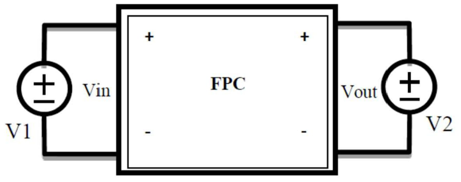
Conventional full power converter (FPC) (e.g. a TSBB converter).
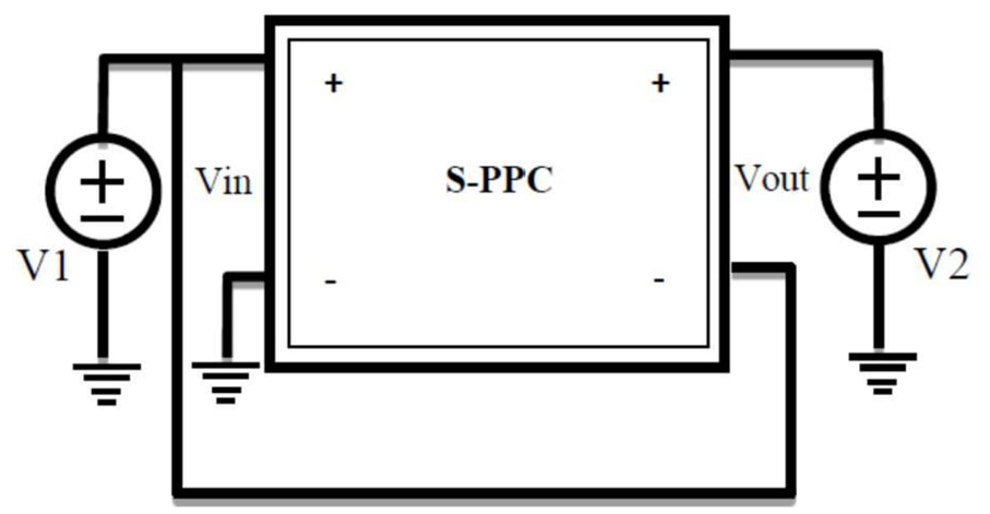
Series connected partial-power converter (S-PPC).
Due to the series connection, the power handled by the S-PPC is a fraction of the output power. Because S-PPC operates as a voltage regulator, S-PPC’s power is equal to regulation power.
Using equations (10)–(15), the power processed by the S-PPC (


It is clear that if the overall efficiency when a full power converter with 90% (
Figure 10 shows the proposed FB/PP S-PPC topology. The difference between the proposed and the original topology presented in Zientarski et al. 17 is that the series connection between the output and input terminals is made through the center tap of the secondary instead of the negative bus. This modification allows the use of electrolytic capacitors since the voltage is unidirectional across it. In the original topology, the capacitor voltage is bidirectional and therefore the capacitor has to be non-polarized type, which is difficult to find at high values at high power applications such as the one presented here.
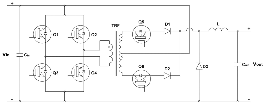
The proposed FB/PP S-PPC topology.
The topology includes four switches at the low-current side, two switches and two diodes carrying the line current, a free-wheeling diode, an inductor, an input capacitor and an output capacitor.
The free-wheeling diode (D3) is added to the conventional circuit to protect the converter from short circuit currents and to enhance the converter switch-on and switch-off ability under load conditions. Without the free-wheeling diode, switching off the converter (especially Q5 and Q6) under load can be harmful to semiconductors. Another necessity of using D3 is to control Q5–Q6 switching duty cycle to achieve current limiting and soft starting.
A modified phase-shift PWM control algorithm is used to control proposed converter. Classical full bridge switching algorithm is used on the primary side of the transformer with duty cycle control to regulate output voltage. The 180-degree phase shifted two PWM signal is applied to Q5–Q6 switches in buck mode where the input voltage is higher than output voltage. On the other hand, in boost mode where input voltage is lower than output voltage, Q5–Q6 switches are in on position in whole period like short circuited. In every working mode, duty cycle value of full bridge side determines converter regulation voltage (±ΔV). A software-based PI algorithm is used to make a closed loop control of output voltage.
Because the proposed partial power converter allows unidirectional power flow, it is placed between battery and load. The proposed converter is not suitable to use a battery voltage regulator between battery charger output and battery groups where power flow is bidirectional. Bidirectional converter topologies are not capable of partial power processing.
Design of FB/PP S-PPC and TSBBC topologies
In order to evaluate and compare the results, a TSBBC and a FB/PP-S converter were designed for the same battery storage system application. Microchip dspic33fj32mc204 digital signal processor was selected and used for control software. This chip allows to control independent PWM outputs and dead time zone. 23 The designs were carried out for 220 V-100 A (22 kW) output with an input voltage window of 180–265 V. The switching frequency was selected as 20 kHz, and the limit ripple values were determined to be as 1 A and 1 V.
Some beneficial studies carried out through literature are about battery management, battery measuring.24,25 Other helpful studies are related boost converters and resonant converters.26–28
For the TSBBC, the minimum duty cycle in the buck mode and maximum duty cycle in the boost mode are calculated as 0.83 and 0.18, respectively. Based on these values, the minimum capacitance and inductance are found by using equations (5)–(9) as 5 mF and 1.87 mH. These parameters along with the real component values selected for the application are listed in Table 1.
Parameters of experimental TSBBC.
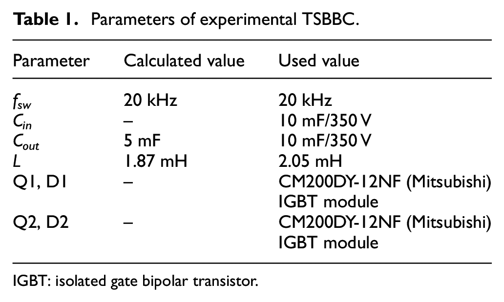
IGBT: isolated gate bipolar transistor.
FB/PP S-PPC can be designed for the same application by using equations (16)–(26). Since the converter power is 20% of the full power,
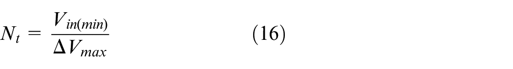
where minimum value of the input voltage (

In order to obtain duty cycle in step-down mode (

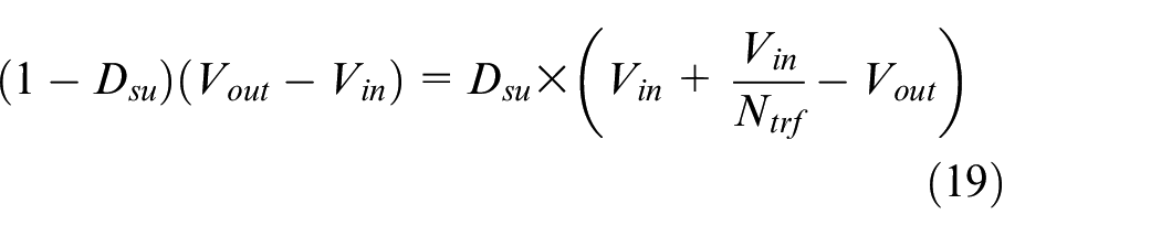
These equations can be simplified as follows
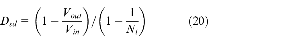
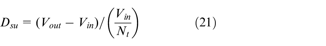
When the extreme voltage values of the input are applied, the minimum and maximum values of the duty cycle are obtained as 0 to 0.22 for the step-down operation and 0 to 1 for the step-up operation.
Filter inductance (

in the step-up mode and as

in the step-down mode.
The largest current ripple occurs at
Minimum value of the filter capacitance (


Similar to the TSBBC, the worst case occurs in the boost mode, and the extreme case is when the capacitor has to supply the load for a whole period. As a result, the minimum value of the capacitor is calculated as 2.5 mF.
Design parameters of the proposed FB/PP S-PPC are presented in Table 2. Capacitance and inductance values sufficiently larger than the minimums were used. The table also lists the semiconductors used in the experimental set-up. As observed from Tables 1 and 2, required capacitance and inductance values are lower for the same design requirements. However, the experimental set-up, which will be presented in the next section, was built-up with the same filter components.
Parameters of proposed FB/PP S-PPC.
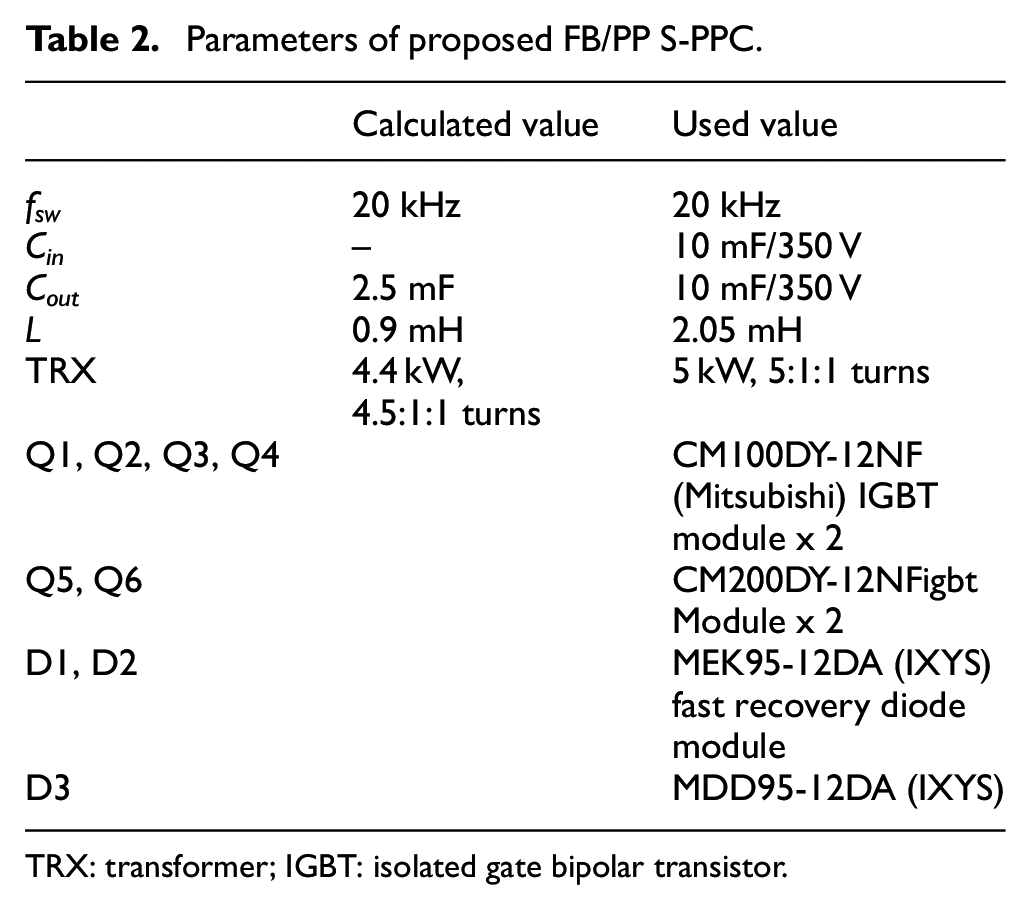
TRX: transformer; IGBT: isolated gate bipolar transistor.
Experimental results and comparisons
Both converters were built and tested to compare their performances. Experimental set-ups are shown in Figures 11 and 12. In order to make a fair comparison between the two converters, the same switching components were used in converters design, as listed in Tables 1 and 2.
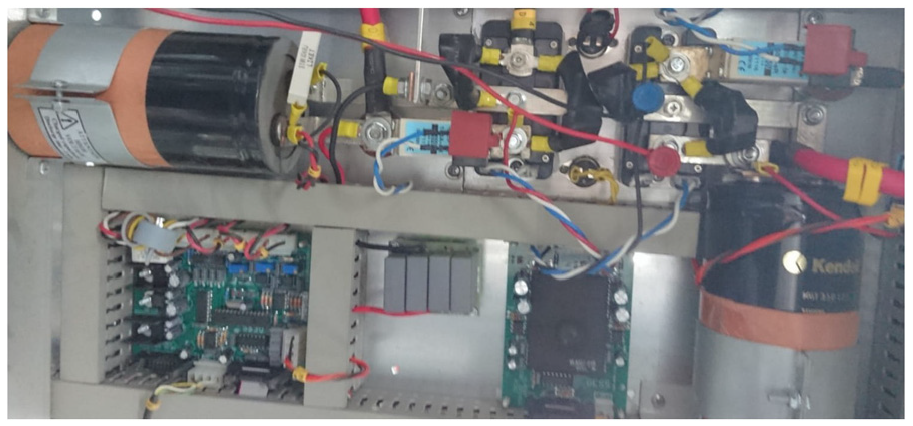
Experimental TSBB converter setup.
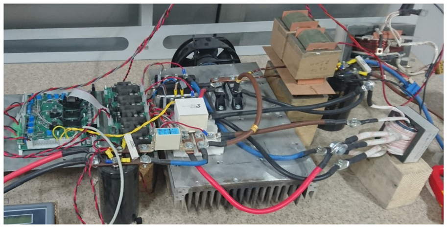
Experimental FB/PP S-PPC setup.
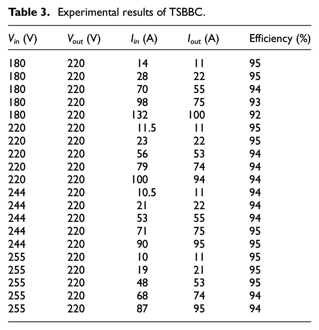
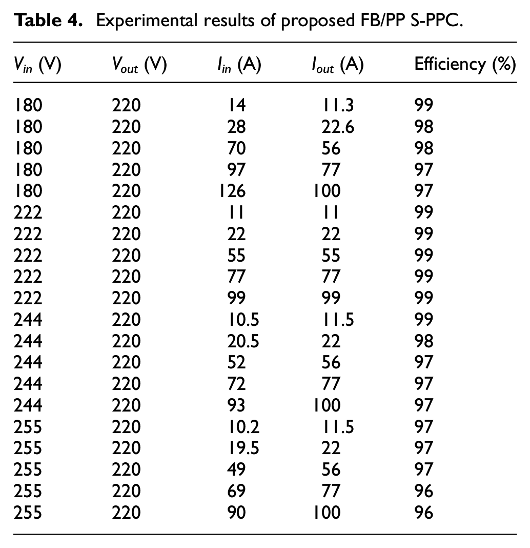
Two converters were tested in various input voltages and output current conditions. Active power, voltage, current and efficiency values were measured with Chauvin-Arnoux DC Power Quality Analyzer (CA-8230). Tektronix DPO-3034 digital phosphor oscilloscope was used to measure signals. Table 3 presents experimental results of implemented TSBBC and Table 4 presents experimental results of proposed FB/PPS-PPC. Figures 21 and 22 graphics were obtained using these table-values. It can be seen from these values and graphics that proposed FB/PP S-PPC has higher efficiency than TSBBC in all various test conditions, especially in equal input and output voltages condition due to series-voltage regulator ability.
Experimental results of TSBBC.
Experimental results of proposed FB/PP S-PPC.
The input and outputs of the converters may include non-active power because of square-wave AC signals of the voltage and the current, but these non-active powers are filtered by the input capacitor (
Figures 13 and 14 show the operation of the proposed FB/PP S-PPC. Voltage between the ground and the transformer secondary rectified point before the L-C filter is seen in Figure 13 in the step-down mode with an input voltage of 255 V, and in Figure 14 at the step-up mode with an input voltage of 180 V.
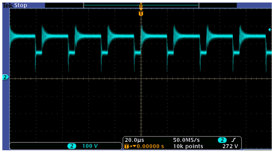
Voltage before the L-C filter (across the D3) of the proposed FB/PP S-PPC in step-down mode with an input voltage of 255 V.
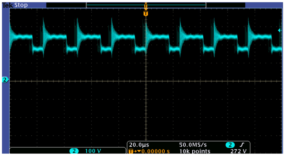
Voltage before the L-C filter (across the D3) of the proposed FB/PP S-PPC in step-up mode with an input voltage of 180 V.
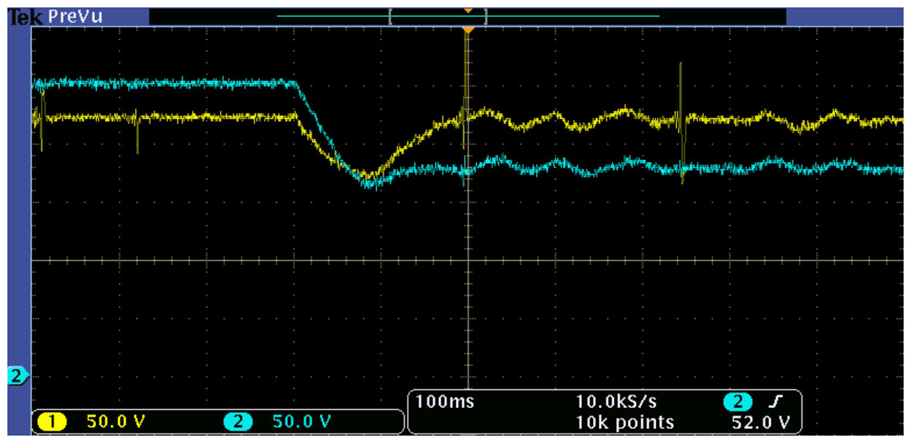
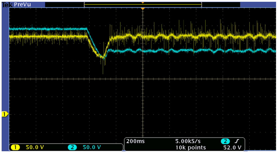
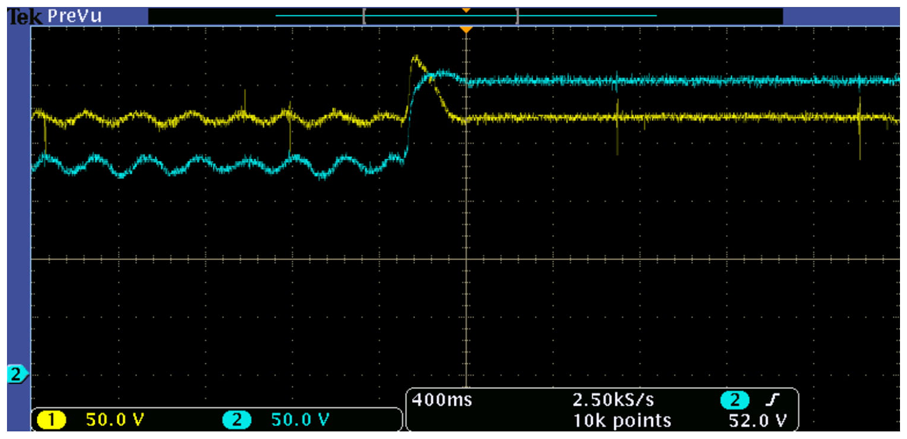
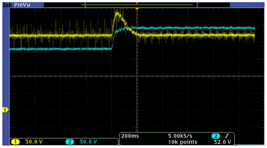
Figure 15 shows the dynamic response of the TSBBC when the input voltage is dropped from 255 to 180 V. Figure 16 shows the response of the proposed converter to the same voltage change. Figures 17 and 18 show the responses of the converters to input voltage increase from 180 to 255 V.
Dynamic response of TSBBC to input voltage drop (255–180 V) (Ch-1: Output voltage; Ch-2: Input voltage).
Dynamic response of the proposed FB/PP S-PPC to input voltage drop (255–180 V) (Ch-1: Output voltage; Ch-2: Input voltage).
Dynamic response of TSBBC to input voltage increase (180–255 V) (Ch-1: Output voltage; Ch-2: Input voltage).
Dynamic response of the proposed FB/PP S-PPC to input voltage increase (180–255 V) (Ch-1: Output voltage; Ch-2: Input voltage).
Figures 19 and 20 shows the dynamic response of the proposed converter to load change from 0% to 100% and 10% to 100%.
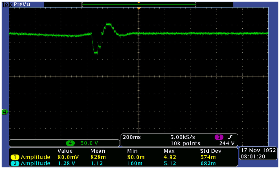
Output voltage of the proposed FB/PP S-PPC to load change (0%–100%).
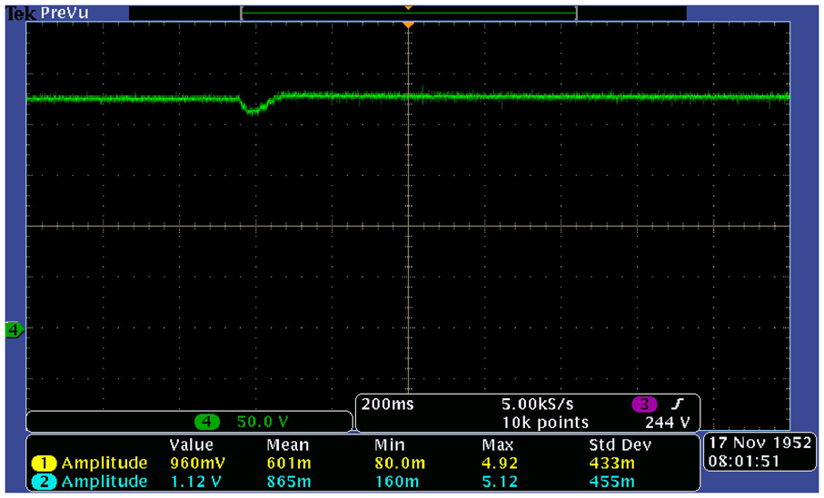
Output voltage of the proposed FB/PP S-PPC to load change (10%–100%).
All dynamic responses were obtained at 22 kW output power with an AC/DC rectifier as the input source to be able to see the worst case responses of converters. The results show the clear advantage of the proposed converter is in the fact that the response is faster. Since both converters were designed for the same amount of ripples, there is no difference in that aspect.
Figure 21 shows the efficiency of the converters for operations with input voltages between 180 V and 260 V, while the load current is kept at 100 A. The proposed converter is more efficient at each operating point as expected, with the highest efficiency is obtained at the rated voltage.
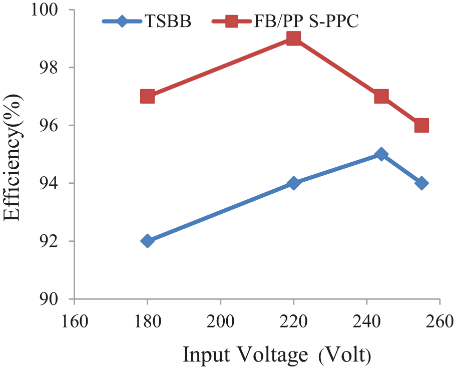
Efficiency curves of two converters versus input voltage.
Figure 22 is a similar plot for the efficiency with the load current is varied while the input voltage is kept at 180 V. The lowest efficiency is obtained at the full current (18 kW).
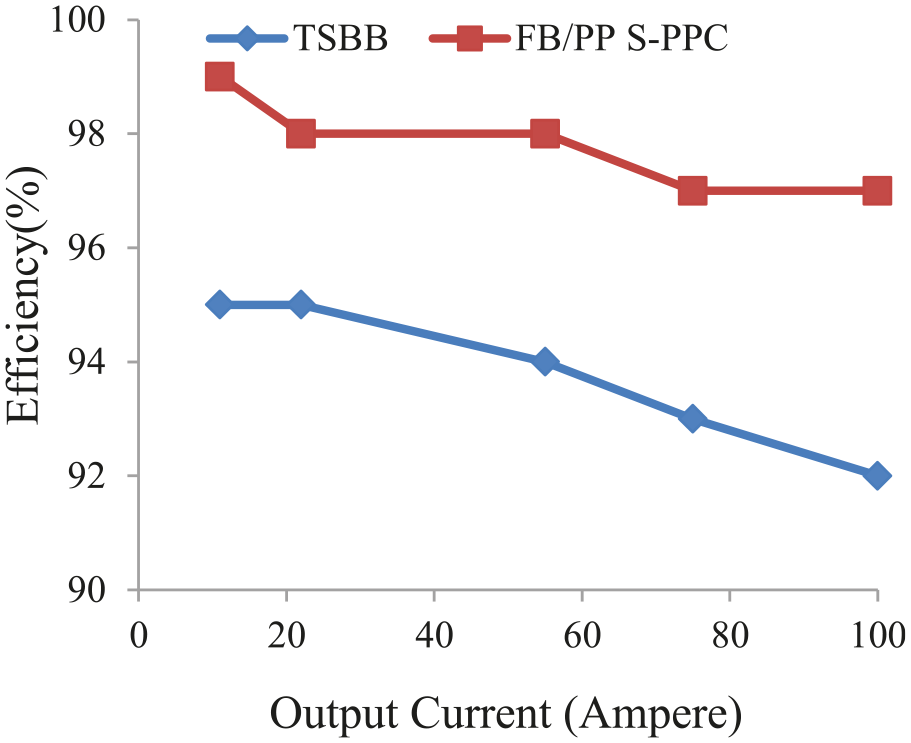
Efficiency curves of two converters versus output current.
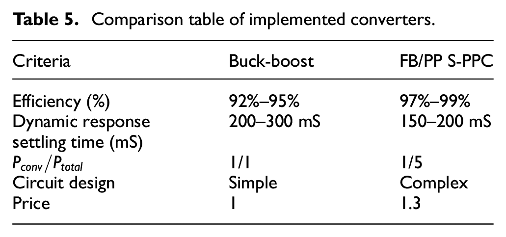
Table 5 summarizes the results to compare the converters. The proposed converter is superior in terms of the efficiency and dynamic response. However, it is more complicated as expected and the cost is about 30% higher than the TSBB converter.
Comparison table of implemented converters.
Conclusion
Two DC/DC converters for industrial BESS were presented in this paper. Industrial BESS have AC/DC battery chargers and load connections. Because of the nature of battery charge–discharge characteristics, there is an unregulated voltage between battery terminals and DC bus. In this paper, two DC/DC converter topologies were designed and tested for the same application. One of the converters is TSBBC and the other one is the proposed full bridge push-pull partial power processing (series connected) (FB/PP S-PPC) converter. The results show that while both converters are better than the simple methods such as the diode dropper method and the float cum boost charger, the proposed converter is also superior to TSBBC both in terms of efficiency and dynamic response. The extra cost and complexity are at manageable levels.
Tests were performed at 22 kW output power. The results show that the proposed converter can also be used at higher power levels. Although this paper presents good study of proposed partial power converter, switching stresses on the Q5–Q6 switches reasoning from series diode’s recovery times are high. Snubber design to get lower voltage spikes on Q5–Q6 switches can be studied in the future works.
Footnotes
Declaration of conflicting interests
The author(s) declared no potential conflicts of interest with respect to the research, authorship, and/or publication of this article.
Funding
The author(s) received no financial support for the research, authorship, and/or publication of this article.