
Abstract
Nondestructive infrared detection of solder defects in solenoid coil connectors was investigated. A detailed experimental setup and a meticulous and repeatable experimental procedure were developed. The experimental methods were firmly based on the application of heat transfer science. Time averaged excess temperature (
Keywords
Introduction
Although surface mount components (SMC) are dominant in electronic assemblies, through hole components (THC) and several other kinds of components are still indispensable for several electronic assemblies. Examples of these components are mechanical components, electrolytic capacitors, connectors, and large inductors. 1 Many non SMC are still hand soldered, but the electronics industry is moving toward fully robotic soldered devices to allow the elimination of human errors and idle time. However, the soldering robotic systems require complex illumination systems, image processing and classification algorithms for soldering defects identification. Several 2D AOI systems have been used with success for the identification of defects in surface mount assemblies.2–5 As mentioned by Richter and Schambach, 6 these systems rely on diffusive reflection of visible radiation and a high contrast between light and dark regions. This makes them inadequate for the inspection of highly reflective and sloped solder joints like those in through hole technology (THT). Fonseka and Jayasinghe 7 showed a successful application of a particular 2D AOI system for the detection and classification of THT joint defects. However, their system relied on a quite perfect illumination of the solders and several complex algorithms for the identification of the different defects studied. Instead, Richter and Schambach 6 proposed a novel 3D AOI system based on specular reflection of visible radiation from the solder joints. Their method showed to avoid the drawbacks of highly reflective surfaces. However, they corroborated the capacity of the method to produce 3D profiles for only unsoldered and good soldered pins. Further studies are required for the actual application of such methodology in the identification of diverse THT solder joint defects.
A methodology not only based on the visible fraction of the electromagnetic radiation spectrum might offer advantages over these AOI methodologies. Infrared thermography nondestructive methodologies8–18 consist of capturing the infrared radiation of the objects under inspection by means of a thermal camera to detect abnormal temperatures and, therefore, defects. When no external thermal excitation is used to manifest the abnormal temperatures, the technique is called passive thermography. If an external thermal excitation is applied, the method is called active thermography. Active thermography is more difficult to apply, because the thermal excitation source highly depends on the object under inspection. Nevertheless, active thermography can evidence defects that otherwise could not be discovered. Several thermal excitation devices have been used (comprehensive classifications of such devices can be observed in Ibarra-Castanedo et al. 8 , Ciampa et al. 13 , and Doshvarpassand et al. 15 ), but heat lamps are the most used non-invasive devices. Similar to AOI methodologies, active infrared thermography illuminates the object under inspection before capturing the images from such object. The difference is that AOI systems use cold light while the thermography systems use heat lamps. AOI systems capture the visible reflected radiation from the object, but thermography systems capture the infrared radiation irradiated by the object. When the thermal irradiation from the lamp reaches an electronic assembly under inspection, the thermal irradiation is absorbed differently by the shiny solder and the rest of the surface of the electronic assembly, providing a high contrast between them in the captured thermal images. The thermal signature captured by the thermal camera will be affected not only by the shape and the radiative properties of the solder, but also by the thermal interaction between the solder and the rest of the surfaces exchanging thermal energy. For example, a solder joint with insufficient solder will probably show a thermal signature with a smaller dark (cold) spot than that of the thermal signature of a good solder joint. Average temperatures of identical regions containing the solder joints and the near area affected by the solder joints will differ among the good and defective solder joints. For instance, the average temperature will be higher for the defective solder joint region. In this way, a comparison between good and bad solder joint average temperatures will allow the detection of a defective solder without the need of complex and lengthy image processing to extract color features pixel by pixel. However, the capacity to detect the difference between the temperatures of defective and non defective regions depends on: the region selected, the amount and quality of thermal irradiation provided, difference of the thermal radiative properties of the solder and surrounding regions, the time of thermal irradiation, the inspection time, the severity of defects, etc. Giron-Palomares et al. 19 were capable to demonstrate that active infrared thermography can be used to differentiate good solder joints from multiple kinds of significantly bad solder joints with temperature differences higher than 1°C in plastic ball grid array components (PBGAC). In their numerical analysis, they considered a quite uniform surface uniformly absorbing heat from a lamp and transferring such heat by conduction to the defects far below such surface. A thermal camera will capture the images from the dark surface approaching a black body in this PBGAC, but it is known that thermal cameras have difficulties to obtain accurate temperatures of objects with highly reflective surfaces (e.g. THT solder joints). Some experimental researches20,21 have shown a fair success of infrared thermography to detect evident hidden defects in BGAs. Nevertheless, the defects are blocked by several objects, and thus visible defects (e.g. solder in the pin side of THTC) should have a better detectability. Bohn et al. 22 investigated the possible detection of visible shiny defects (unwetted, unsoldered, bended, and lifted leads) in a SMC (QFP) by means of active infrared thermography. They provided heat to the neighboring regions of the solder joints in the leads, and used the different thermal conduction behaviors of defective and non defective solder joints to obtain different thermal signatures. Unfortunately, they were capable to detect only completely open connections. In this research, the capacity of infrared thermography to detect solder connector defects of a solenoid coil was investigated. The shiny solder joints in the solenoid coil are much bigger than the leads in a QFP, separated from each other by a large distance, completely visible, and surrounded by a dark opaque plastic surface. These characteristics of the connector solder joint make it a good candidate for nondestructive active infrared thermography detection. The main objective of this research is to establish the adequate infrared thermography detection methodology that could provide a good detection of several defects encountered during the soldering of the connector. Moreover, the methodology established by this research can be used as a guide for the development of infrared methodologies to detect several other kinds of similar defects encountered not only in the electronics assembly industry, but also in several other manufacturing industries. This methodology can allow better automation of production lines by reducing human errors and idle time. Consequently, this will allow better and cheaper products for an affordable and better daily life.
Materials and methods
To allow a high possibility of detecting the connector solder joint defects, the characteristics of the infrared thermography detection procedure should be established according to the connector and the carrier characteristics. The detection of the connector solder defects was performed by following the next methodology:
Establish the thermal and geometrical characteristics of the connector solder joint and defects, as well as those of the carrier;
Decide the heating (illumination) source to use and its characteristics;
Establish the characteristics of the used thermal imager;
Establish the best way of interaction among the connector solder joint, thermal imager, and heating source to ensure good thermal signatures, as well as heating and thermal measurement repeatability;
According to previous step 4, build an experimental infrared thermography nondestructive testing system;
Perform several experiments with the testing system by varying heating time and kind of defect;
Study the experimental results and determine the experimental parameters and thermogram processing procedure that give the best detectability of defects;
According to the detectability of the defects, determine the capacity of infrared thermography to detect the connector solder joint defects.
Steps 1–3 of the methodology shown above are described in Infrared thermography nondestructive system basis. Steps 4 and 5 are discussed in Experimental setup. The experimental procedure used to complete step 6 is presented in Experimental procedure. Finally, Results and discussion and Conclusions are described in Results and discussion and Conclusions. Moreover, a block diagram condensing this research methodology is presented in Supplemental Material 1.
Infrared thermography nondestructive system basis
The connector under study is a spade connector in a solenoid coil (see Figure 1) that is encapsulated with a plastic after the windings copper wire ends are attached and soldered to the internal bended ends of the leads. The copper wire is coiled on the bended part of the lead and then soldered to generate a strong bond difficult to break. The soldering process might be performed by hand or machine. Hand soldered joints are inconsistent, but any solder defect can be judged and immediately fixed by the technician. As the copper wire is coated by a material that repels the solder, enough solder is added so the solder completely covers the copper wire and the bended lead. This process produces a good big solder bump joint that is in contact with the plastic surrounding the bended lead base and covers the whole bended lead as well as its copper wire (see SJ1 in Figure 2(a)). To avoid any misjudgment or neglect of the technician on the quality of the solder joint, companies are replacing hand soldering for machine soldering. Considered solder joint defects are shown in Figure 2. Defective solder joints do not have enough solder to cover: down below the copper wire on the bended lead (SJ2, Figure 2(b)), the bottom of the bended lead (SJ3, Figure 2(c)), or the whole bended lead and its copper wire (SJ4, Figure 2(d)). While the solder, the leads and the copper wire are shiny metals (high reflectivity, low emissivity, high thermal conductivity), the disk carrying the leads is a dark plastic (low reflectivity, high emissivity, and low thermal conductivity). Thus, this high difference in thermal properties allows strong interaction among such components. For example: the big solder bumps in good solder joints (SJ1) may cause lower temperatures surrounding the leads (more thermal radiation is reflected); no solder (SJ4) may provoke higher temperatures (less thermal radiation is reflected); and no solder only on the bottom of the bended lead (SJ3) will mainly affect the interaction by thermal conductivity between the carrier and the solder, provoking probably higher temperatures than those in SJ1 but lower than those in SJ4. In the case of solder joint SJ2, less thermal radiation is reflected than in the solder joints SJ1 and SJ3, but more than in SJ4; moreover, there is not interaction between the solder and the carrier by thermal conductivity (this is similar to SJ3), and the difference with SJ4 on the thermal radiation reflected might be small. Therefore, it is difficult to draw a hypothesis on temperature observations for SJ2 without actual experimental data. Also, the dimensions of the carrier and the leads (see Figure 1(a) and (b)) are not that high and it is unclear the effects of such dimensions on thermal exchange and thermal signature clarity. However, it is clear that differences among the thermal signatures of the solder joints might be not extremely high, showing the importance of properly locating the solder joints with respect to the thermal source and the thermal camera.

Solenoid windings: (a) connector front view, (b) connector left side view, (c) suspended connector, and (d) prepared connector for experiments.

Schematic views of the connector solder joints modeled: good (a) SJ1 and defective, (b) SJ2, (c) SJ3, and (d) SJ4.
In active thermography nondestructive testing, noncontact heat lamps (optical thermography) are preferred to provide energy to the object under inspection. According to the lamp and its operation, optical thermography can be divided in pulsed thermography, lock-in thermography, and step heating thermography.8,13,15 Pulsed thermography and step heating thermography are one time excitation methods monitoring thermal transient response, while lock-in thermography is a modulated excitation method monitoring steady thermal response. 9 Lock-in thermography is less affected by the multiple problems affecting the other methods (e.g. nonuniform heating, heat source radiation effects, reflections from the environment, emissivity variations, and surface geometry variation), but it is slower and more complex to perform.8,15 Expensive flash lamps can be used by pulsed thermography to produce short pulses (ms) for near surface defects in very fast detections during cooling. To reduce the effects of nonuniform heating and reach deeper defects, cheaper heat lamps can generate: pulses higher than 1 s in detections during heating and cooling, and long pulses (tens of seconds) in detections during cooling. Lock-in can reach relatively deep defects in a much more complex detection procedure. Step heating has similar capabilities to long pulse thermography, but it is performed during heating and highly affected by the heating source radiation effects. From these optical thermography methods above, long pulse thermography can allow a high penetration of the thermal radiation, while avoiding a quick dissipation of thermal energy because of the thermal exchange of the solenoid with the surroundings. Quick dissipation reduces the duration of the defect thermal signature visibility. Halogen lamps can provide thermal irradiation for long times, and they are cheap and easy to adjust to thermal, positional, and dimensional requirements. These lamps allow long times of heating that might clearly evidence the different thermal behavior of the solder and the carrier for a long time. It has been proven 23 that quartz halogen linear lamps can provide extremely repeatable amounts of energy on the surface of an inspection object, when the positions of the lamp and the inspected object are consistent among different measurements. Therefore, a 500 W quartz halogen linear lamp (from now on referred just as “halogen lamp”) like that tested in 23 was selected as the illumination source (see Figure 3) to perform long pulse heating thermography.

Schematic view of the quartz halogen linear lamp.
The thermal imager available for this research is a FLIR T660 with a thermal resolution of 640 × 480, accuracy of ±1°C or ±1% of the reading, thermal sensitivity of 0.02°C, and a minimum focus distance of 0.25 m. Locating the camera as close as possible to the connector bended lead can provide about 1054 temperature measurements uniformly distributed in the solder joints. Thermal camera’s temperature measurements are greatly affected by the thermal radiative properties of the inspected objects and the surrounding bodies participating on the radiation exchange with the camera and the inspected object. Actual temperatures of opaque objects with low reflectivity and high emissivity are accurately measured by the thermal camera. Real temperature of opaque objects with high reflectivity and low emissivity (ε < 0.5) is practically impossible to measure. The reason is that the radiative energy from surrounding objects is reflected by the shiny object toward the thermal camera lens, and thus the camera measures an apparent temperature caused by emission and reflection. The shiny connector solder falls into this category of highly reflective opaque objects. The thermal camera can show an accurate temperature of the carrier, but an apparent temperature of the connector. Now, this might be actually helpful for the detection of the defective connector solder joint, because a hot solenoid coil in cool surroundings would present a high thermal contrast between the carrier and the connector solder joint. In this way, the differences in the irradiated energy from the solder joints and in the thermal interaction between the carrier and the solder joints can permit a classification of the solder joint type. Nevertheless, it is imperative that: the surroundings have uniform high radiative emissivity, no external sources of high irradiation exist, and the solenoids are located in the same location (with respect to the camera and the surroundings) for each thermogram acquisition.
Experimental setup
The halogen lamp can provide repeatable amounts of energy to the connector, but the positions of the connector and the lamp with respect to each other should be the same among different measurements. Giron-Palomares et al. 23 developed a lamp holding structure with the capacity to: hold the lamp’s frontal face consistently aligned with the horizontal plane, align sample’s central axis to lamp’s central axis, and change lamp’s height; the technique was proven to be excellent, repeatable, and avoiding noise. 23 A lamp holding structure with the same dimensions and characteristics was used in this research. The connector can be aligned in different ways with respect to the frontal face of the lamp. However, if the thermal energy is provided to the connector top face: the thin thickness of the carrier would allow moderate variations of temperature in the vertical direction, a high amount of energy would be transferred to the connector components, higher amounts of energy would directly reach the solder joint, stronger thermal interaction between solder joint and carrier could occur, and the face of the carrier disk would be easier to align to the frontal face of the lamp. Moreover, it is important that only the radiative energy directly coming from the lamp hits the connector face, in order to avoid any other significant thermal gradients reducing the interaction between carrier and solder joints.
As in the case of the alignment between the lamp and the connector, the camera lens and the connector top face should be aligned horizontally, because this permits to record the solder joint’s thermal signature with the plastic carrier’s top face as the background. Consequently, the solder joint shapes would be very clear because of the high contrast between the thermal distributions of the carrier and the solder joints. Because the camera sensors will catch reflected radiation from the solder joint, the radiative energy irradiating the solder joints should come from objects at low temperatures with respect to the carrier temperature, and be consistent among every temperature acquisition performed. In addition, any reflected radiative energy from other objects besides the connector should be eliminated to avoid any detrimental effects in the thermal profile recorded by the thermal camera. Finally, the acquisition of the thermal profile should be performed after the heating of the connector (long pulse thermography), in order to avoid any damage caused to the camera’s sensors by the radiation from the high temperature tungsten filament, and thermal artifacts in the thermograms.
The solenoid connector is originally suspended by the two wire terminals of the solenoid windings (observe Figure 1(c)). Consequently, the motion of the solenoid coil would impart excessive motion to the solenoid connector, hindering uninterrupted connector alignment. Thus, the solenoid coil was prepared in order to allow the repeatability of the experimental procedure (see an experimental specimen in Figure 1(d)). The carrier disk was pulled to the top of the solenoid bobbin in such a way that the external leads were inside the internal bobbin cylinder and the bottom face of the carrier disk was in contact with the top of the bobbin. The carrier was securely attached to the bobbin by using a copper wire with the same characteristics as the solenoid windings. This allowed a good alignment of the carrier disk, and no motion of such disk during the development of the experiments. Moreover, a bright circular spot was painted on the top of the bobbin to allow an identical area selection on the thermograms (refer to Thermogram analysis procedure for details). This extensive preparation of the solenoid coil was done only to allow a good repeatability in the experiments and a clear evaluation of the capacity of the thermal signature to differentiate solder joints. On a manufacturing site, no preparation of the solenoid coil is allowable, but a support for the connector can be designed and properly integrated into the manufacturing process according to the particular manufacturing site characteristics. Also, the thermal radiative properties of the solder joint surfaces should be not significantly different among different solenoid coil models, in order to avoid significant effects of such variability in the produced thermal signatures. Accordingly, the solder joints were generated by employing the same material (Sn99.3/Cu0.7) and production procedure. The resulting solder joint surfaces were confirmed as very similar without stains, remaining flux, or any other factor significantly altering their thermal radiative properties. This ensures that the variability of the thermal signatures of the different solenoid coil models is an effect of the solder joint geometry as well as its interaction with the surroundings.
According to the few paragraphs above in this subsection, it would be advantageous to perform heating and acquisition in two different areas, because these two processes have some quite different requirements. Nevertheless, the two areas should be somehow connected to allow a quick movement of the connector and, thus, avoid significant thermal contrast reduction because of the cooling process. In a factory, the solenoid coils might be moved by means of conveyors from one to another subsequent in-line manufacturing automated processes. Of course, the inspection of the solder joints shall be one of those processes, and, therefore, the heating and acquisition areas should follow immediately each other. Accordingly, a solenoid bobbin holding fixture attached to a three-rail slider connecting both areas was designed to simulate the inspection process. The experimental setup for the inspection process can be observed in the Supplemental Material 2. The heating area was open to the environment to allow its quick cooling, because the heating process is not significantly affected by the surroundings when no high currents of air and no high additional sources of thermal radiation exist. 23 On the contrary, the temperature acquisition might be affected by the hot heating area elements; thus, the acquisition area (from now on referred as cooling chamber) was designed as an enclosed space with sliding doors to allow the solenoid holding fixture entrance. The walls and the floor of the cooling chamber were produced of Plexiglas, while its roof was made of Styrofoam with a round perforation for the access of the lens of the thermal camera. The internal surfaces of the cooling chamber were painted matte black to allow a minimum of radiative transmission and reflection, but maximum uniform radiative emission toward the solenoid and its connector. This ensured a consistent radiative energy irradiating the solder joints among every temperature acquisition performed, and a minimum of detrimental effects in the thermal pattern recorded by the thermal camera. The temperatures of the air inside the cooling chamber, as well as those of the internal surfaces of the walls, were monitored during the heating process by using thermocouples, and no significant increment of temperatures was observed. The air and the far walls in the cooling chamber registered temperature increments below 2°C, while the wall beside the heating area showed temperature increments below 4°C. The end of the rail 3 pointing toward the cooling chamber was attached by means of a linear spring to the stopper of the rail 1, while the end of the rail 3 pointing toward the heating area had a protuberance contacting a turnable locking mechanism at the front of the heating area. The release of such mechanism frees the slider, whose linear movement opens the sliding doors and locates the solenoid bobbin holding fixture on its acquisition location in about 2 s.
The solenoid bobbin holding fixture performs several important functions, and it is composed of two parts: bobbin support and reflecting cover. The bobbin support was designed to hold firmly the solenoid bobbin avoiding high vibrational motion and to facilitate a repeatable positioning among experiments. Markings in the bobbin support and the bobbin samples allow such positioning. On the other hand, the reflecting cover (made of Styrofoam and coated in aluminum foil) ensures no overheating of the solenoid coil. Overheating of the solenoid coil during experiments can unreasonably increase the waiting time between consecutive experiments in a repeatability study. The cross laser beam of the lamp holding structure 23 permits the assurance of the alignment between the solenoid coil vertical axis and the heating lamp vertical axis. All the horizontal facets of the experimental setup components (e.g. solenoid spade connector carrier, lamp, and camera lens) were perfectly aligned, by means of bubble levels, to the large flat horizontal base supporting the experimental setup.
To ensure no highly different initial temperatures and no initial thermal unsteadiness in the experiments, K-thermocouples were located (see detailed locations in Figure 1 and Supplemental Material 2) in the internal surfaces of the walls of the cooling chamber (Tf, Tr, Tl), the ceiling of the cooling chamber (Tt), the air in the proximity of the lamp (Tair), the left external straight lead in the spade connector (Tll), and the bottom face of the connector carrier disk (Tc). CONCEPT ENGINEERING model FRM-200-K thermocouples with a diameter of 9.5 mm and a thickness of 1.8 mm were used for Tf, Tr, Tl, and Tair, while very small OMEGA KK-K-30-72 thermocouples were employed for Tt, Tc, and Tll.
Experimental procedure
The main purpose of this research is to assess if the thermal signatures of the different solder joint defects can be discriminated from a good solder joint. To accomplish this, it is important to provide high thermal contrast during short inspection times. As determined by, 23 high distances from the lamp to the object under inspection increase the time needed to provide adequate amounts of energy. This increment also augments the full inspection time, and therefore the distance from the lamp (Hl) was established as the shortest distance possible (200 mm). The heating time (th) served as the parameter to vary the amount of heat provided to the sample. A study of the effects of the heating time on the difference between non defective and defective thermal signatures can establish an adequate heating time for a successful detection of defects. The heating times used were: 12, 20, 36, 52, and 78 s. Thermal contrast is expected to be high, because the thermal radiative properties of the solder joints and the carrier are highly contrasting. It is important to ensure repeatability of the thermal signature acquisition by performing several experiments for each solenoid connector solder joint. The camera was located in such a way that the vertical distance from the frontal edge of the infrared lens and the top of the connector bended lead (Hcam) was about 300 mm. For example, this distance provided more than 1733 temperature measurements uniformly distributed in a circular ROI enclosing SJ1 (around 28 measurements/mm2) with a close-up of 1.6x. Other significant settings of the infrared camera were an emissivity of 0.96 (i.e. the emissivity of the black opaque plastic carrier disk) and a reflected apparent temperature equal to the average of the readings of the sensors monitoring temperature inside the cooling chamber.
With the aim to provide heating and thermal signature acquisition repeatability, the same experimental steps (Supplemental Material 3) were closely followed to complete every single experiment of this investigation. About 120 experiments (six solder joint models, four experiments per model, and five heating times per model) were performed (the experimental sets of data generated can be accessed in Research Data 1–3). A minimum of 30 min (th = 20 s) and a maximum of 2 h (th = 78 s) were determined for the time interval between consecutive experiments. This waiting time is needed, because the baseline temperatures of the solenoid coil should decrease and reach those of the previous experiment. On the manufacturing site, this waiting time should not be needed, because each inspection is performed in a different cool solenoid coil. The methods developed here hold several aspects allowing a nondestructive detection technique that is not unnecessarily complicated, scientifically sound, and promising for its actual application in a manufacturing site.
Results and discussion
This section presents the results of the experiments performed. The first subsection presents representative thermal images of the four solder joint models at the end of heating for a particular heating time and a discussion of: the characteristics of such images, the adequate processing procedure, and the proper analysis to study the capacity to discriminate defective solder joints from the good solder joint. The second subsection describes the studies to evaluate the discrimination of solder joints, as well as a complete discussion on such matters.
Thermogram analysis procedure
Representative thermograms for the bright solder joint models at the end of heating are presented in Figure 4. The painted bright spot can be seen at the bottom of the thermograms as a dark spot (a low temperature region that reflects a significant amount of the incident thermal radiation). Similarly to the bright spot, the reflecting cover thermal signature can be observed in the bottom corners of the thermograms as dark regions (low temperature regions). The effects of different amounts of energy absorbed during heating by the solenoid coil samples were perfectly caught by the thermograms. This difference is clearly caused by the different geometry of the solder joints and their different interaction with the surroundings. The thermal signature of SJ1 (Figure 4(a)) is quite different from those of SJ2 and SJ4 (Figure 4(b) and (d)), but it is quite similar to that of SJ3 (Figure 4(c)). The wound copper wire is visible at the middle of the bended lead in SJ2 and SJ4 (Figure 4(b) and (d)), but hidden by solder in SJ1 and SJ3 (Figure 4(a) and (c)). The effects of the solder joints in the carrier disk can be observed as: a kind of a ring surrounding the solder joint in SJ1 and SJ3, and an ellipsoid at the base of the bended lead in SJ2 and SJ4. It can be also observed that more reflective surfaces (solder, leads, and copper wire) clearly present lower temperatures standing out from the high temperatures of the plastic dark carrier. Traditional pulsed thermography post acquisition techniques can be divided in qualitative and quantitative analysis. Thermography qualitative analysis focuses on detecting the defects, while thermography quantitative analysis focuses on the characterization of the defects. These complex post acquisition techniques were conceived to 8 : determine the unknown location of a defect on the surface of a quite homogeneous and wide inspection area; diminish the effects of nonuniformities in surface heating, reflection artifacts and emissivity variations; and determine thermophysical parameters and defect’s depth. Details on such complex post acquisition techniques can be observed in.8,24,25 In this research thermography methodology, the connector solder joints location is known, reflection and emissivity differences among the connector components are required for good contrast, and the solders are visible. Therefore, the selection of a region of interest (ROI) and establishment of a characteristic parameter for such ROI can suffice to distinguish the good solder joint from the defective solder joints.
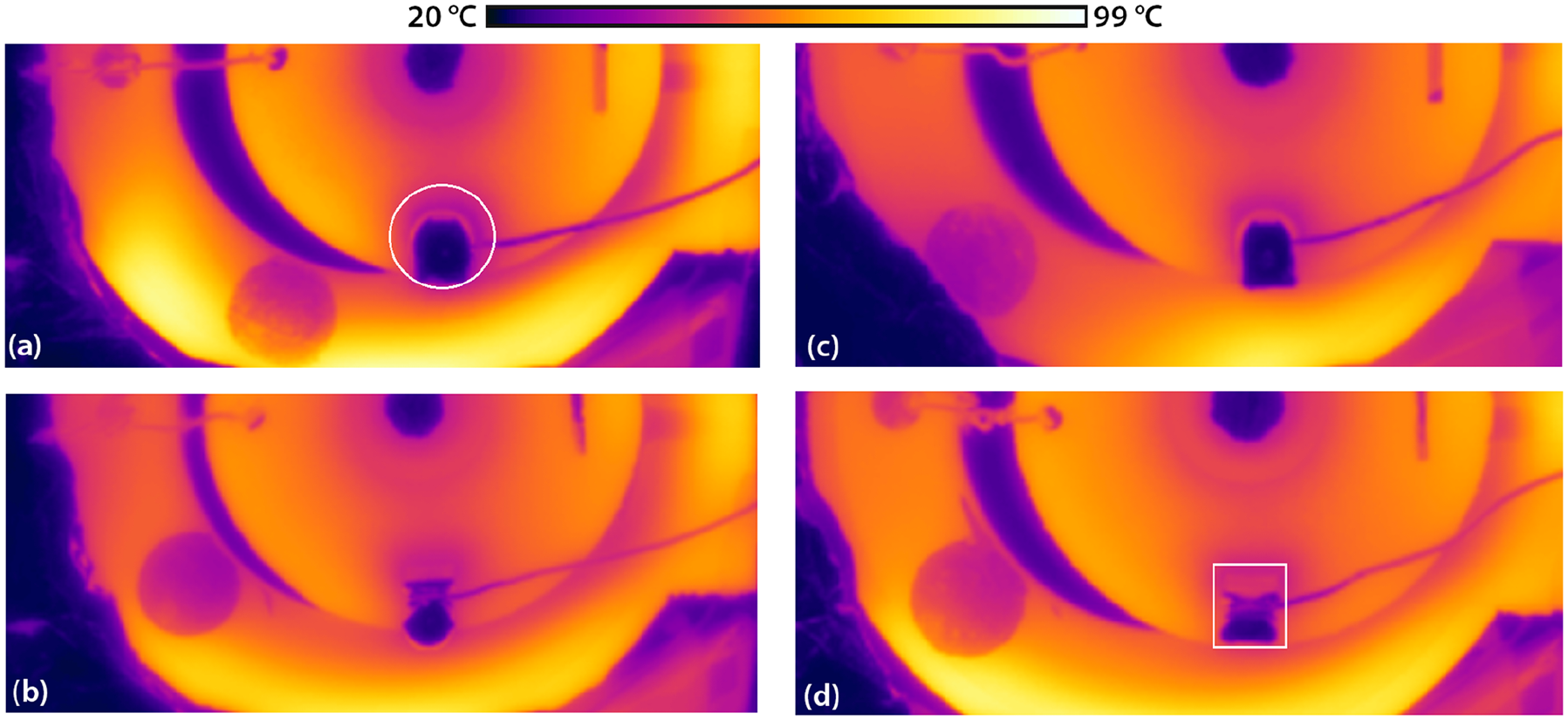
Thermograms for: (a) SJ1, (b) SJ2, (c) SJ3, and (d) SJ4. SJ1 is a good solder, while SJ2, SJ3, and SJ4 are defective solders; circular and rectangular white geometries are examples of ROIs for the acquisition of temperature.
The selection of the region of the thermograms directly affects the capacity of such region of interest (ROI) to adequately characterize the solder joints. In general, the ROI is selected according to its potential effect in the process under study. For example, nose, cheeks, forehead, and lips might be the possible ROIs experiencing a significant change in temperature when the mood of a human is altered, 26 chest, back, face shoulder arms, and legs might be significant ROIs characterizing people during endurance exercising, 27 the rolling bearings should be the ROIs for the study of nano grease performance in bearings under transversal loads, 28 and different regions of a saddle may be the ROIs to assess the fit of such saddle during horse riding. 29 In this research, it is clear that the regions characterizing the solder joints during cooling are the solder joint itself and the near surrounding area. Inclusion in the ROI of the effects of the solder joints in the carrier disk might significantly increase the discrimination of SJ1 with SJ2 and SJ4, but not with SJ3. As determined by, 19 a ROI as closest as possible to the thermal signature of the solder joint in the surface of a plastic ball grid array electronic component was required for a good discrimination. Circular and rectangular areas were tested as possible ROI (examples of such ROIs can be observed in Figure 4). The circular area (45 pixels in diameter) enclosed the good solder joint (SJ1) and the region of the carrier affected by such joint, while the rectangular area (31 pixels × 34 pixels) narrowly enclosed the good solder joint (SJ1). Parameters characterizing the ROI are usually the minimum, average, and maximum of the temperatures. 27 The average temperature is the most adequate parameter for this research. This parameter can account for the low temperatures of the different portions of the solder, copper wire, and leads, but also for the high temperatures of the different portions of plastic carrier contained in the ROI. The size of the circular bright spot painted on the top of the bobbin was verified to be the same in the thermal images for each experiment, in order to confirm no variations on the extend of the region selected by the ROI. Identical ROI size for all solder joint models allowed the unbiased comparison among solder joint signatures. For example, the identical ROI shows more of the carrier, copper and leads in SJ3 than in SJ1, which can make the captured thermal signature difference between such solder models evident. Also, the identical ROIs simplify the thermal image processing.
A minimum of 420 thermograms (a thermogram per second) were recorded for every single experiment. The temperatures of the regions of interest (a minimum of 1054 temperatures per ROI) were extracted from every single thermogram (Research Data 4 shows an example of the excel file generated by the extraction) and then average temperatures were determined (the experimental sets of average temperature data can be obtained from Research Data 1–3). Figure 5(a) shows the temperatures measured during four experiments for SJ1, a heating time of 52 s, and a rectangular ROI. The temperatures at the beginning of the experiments were not exactly the same among experiments, and this can be clearly seen in Tair (these temperatures are in an interval of about 2°C for the four experiments). Starting temperatures for Tc and Tll are also in an interval of about 2.5°C (observe the 10 s of baseline before starting of heating). These effects of such temperature variations should be eliminated to avoid their effects on the discrimination of the solder joint models. Giron-Palomares et al. 23 successfully eliminated effects of variable initial temperatures by defining a temperature difference determined by subtracting the initial temperature reading from the subsequent readings in a particular temperature sensor. In this case, a temperature baseline was recorded for 10 s, and, therefore, the minimum temperature reading during such baseline was used as the subtracting temperature. Accordingly, an excess temperature was defined with the next equation:

where θ is the excess temperature, T is temperature reading, and Tmin is the minimum temperature observed during the experiment. The resulting θ data for this case is shown in Figure 5(b). It can be clearly seen the improvement in the repeatability of the experiments, and therefore θ is a better parameter for the discrimination of the solder joint models. In consequence, all of the subsequent analyses were performed by using θ. By further examining Figure 5(b), it can be observed that θc > θll > θSJ1. The high capacity of the carrier disk surface to absorb and storage thermal radiative energy is the cause of its highest temperature. Meanwhile, θ ll is higher than θ SJ1 , because the infrared camera is measuring an apparent low temperature of the solder joint. The difference among these three temperatures will reduce as the time growths and completely disappear at steady state (the curves at 420 s are already quite close). These excess temperature curves also display the nature of the whole detection process (baseline followed by heating and then cooling). Moreover, θ c increases faster than θll;θ c is measured at a location just below the carrier plastic, while θ ll is measured in a point below the solder, carrier and a fair amount of the lead (see locations at Figure 1). These two excess temperatures are mainly monitoring temperatures to ensure the consistency of the experimental procedure and the infrared camera acquisition procedure, respectively. As θ c is located in a point far from the solder and leads, it is a good parameter to assess the consistency of the experimental procedure among different solder joint samples. In the case of θ ll , this excess temperature should be consistent with those temperatures acquired by the infrared camera of the solder joint regions. Indeed, θ SJ1 is consistently lower than θ ll , because the ROI is capturing low temperatures from the reflective solder surface (see Figures 4 and 5).
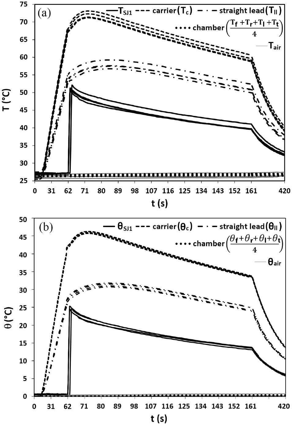
Experimental results for: (a) temperature and (b) excess temperature (θ). SJ1, rectangular ROI, and th = 52 s. Subscripts in variables: f, r, l, and t denote readings of the K-thermocouples on the internal surfaces of the dark chamber; ll and c indicate readings of miniature K-thermocouples inside the solenoid; “air” indicates readings of a K-thermocouple in the air surrounding the experimental setup; and SJ1 represents the temperature of the ROI obtained by the infrared camera. Observe the different time scales for 0 s < t < 62 s and 161 s < t < 420 s.
Supplemental Material 4 shows the excess temperature curves for the solder defects models and a heating time of 52 s. An almost identical value (repeatable) of θ c at the end of heating for all the solder joint models can verify the consistency of the experimental procedure among different solder joint samples. A percentage of repeatability can be determined as follows:

where
The temperature parameter used for the discrimination is as important as the ROI selection in the infrared camera. Although a single value of θ at the beginning of cooling could be used as discrimination parameter, this value might be inadequate because of several variabilities existing a few seconds after the beginning of cooling. Among such variabilities are: camera auto focus adjusting to the higher temperatures as the fixture arrives, a little vibrational motion of the fixture after impacting the rail stopper, and a possible significantly different initial cooling temperature (caused by a little variation in the time the fixture arrives, and the extremely high temperature gradient of the solder joint a couple of seconds after the starting of cooling). These variabilities were avoided by selecting θ values 4 s after cooling starts (t0). On the other hand, selecting an interval of values of θ instead of only one value is vital, because the cooling process is directly affected by the characteristics of the solder joint and its interaction with the surroundings. Nevertheless, this interval should be short enough to allow competitive inspection duration. Also, the difference in thermal behavior among solder joints reduces as the cooling time advances. To use a single parameter for the discrimination analysis (see equation (3)), a time averaged value (

First, the repeatability of the
Discrimination analysis results
The time average values (
Multi-comparison study results for a rectangular ROI and a time integration interval length of 30 s.

th: heating time, p: probability of being the same with a 95% level of confidence,

Multi-comparison among solder joint models for heating times of: (a) 12 s, (b) 20 s, (c) 36 s, (d) 52 s, and (e) 78 s. Rectangular ROI, and a time integration interval length (ti) of 30 s. A constant horizontal-axis interval length of 14°C was used in all the plots.

Minimum difference in time averaged excess temperature (
The minimum difference in
It is clear that the temperatures of the bright solder joint regions are only apparent temperatures, and that temperatures close to the real temperatures of such regions can be obtained only after greatly reducing the solder joint reflectivity. Emissivity variations and reflective artifacts are a problem in the traditional pulsed thermography application, because they reduce the capability to adequately distinguished defects and accurately characterize the defects in a quite homogeneous and wide inspection area; therefore, it is common to paint such surfaces to achieve a homogeneous emissivity near to 1. 8 When real temperatures need to be monitored in devices (e.g. to ensure safety and well controlled processes), it is also common to paint devices. In this research thermography technique, the temperatures generated are not harmful for any component. Moreover, painting the surfaces will reduce the contrast of the originally reflective surfaces not only in the thermogram, but also during the exchange of thermal energy. SJ1 and SJ3 were painted matte black in order to corroborate these adverse effects of a nonreflective solder joint surface not only on discriminability, but also on the whole infrared thermography inspection process. The main problem encountered after painting the solder joint surface was the difficulty to select the ROI from the thermal image, because the contrast between the carrier disk and the solder joints in the thermograms was greatly reduced (examples of thermograms for these two solder joint models at the end of heating are presented in Figure 8). Also, it can be corroborated that the painting allows a higher temperature display of the solder joints in the thermograms (unpainted solders look much darker than the painted solders).

Thermograms for (a) SJ1-bk and (b) SJ3-bk. bk means solder joints are painted matte black.
The experimental set of averaged temperature data for the painted models can be accessed in Research Data 3. Figure 9 shows the results on θ for four experiments performed for the painted SJ1 and SJ3 by using a rectangular ROI to acquire temperatures from the camera and th = 52 s. An excellent percentage of repeatability smaller than 1.5% can be determined for θ c at the end of heating for the painted solder joints set of data, therefore verifying the consistency of the experimental procedure. Additionally, with exception of those of the solder joints (θ SJ ), the other curves are quite similar in order of magnitude with those of the unpainted solder joint models (compare to Figure 5(b) and Supplemental Material 4(b)). The excess temperature values for the painted solder joints are much higher than those for the unpainted solder joints, because the camera is mainly measuring radiation emitted, instead of a combination of reflection and emission. A slight change in the transient thermal behavior of the measurements (θ ll and θ SJ ) affected by the painted regions was observed too; the excess temperature increases faster, achieves higher values and cools faster, because the painting increases the role of thermal radiation on the thermal exchange process (thermal radiation exchange varies with the fourth power of temperature). The excess temperature for the solder joints shows the highest values with exception of θ c , because the carrier disk has similar radiative thermal properties but lower thermal conductivity than the solder joint. Heat is transferred faster from the surface of the solder joint than from the surface of the carrier disk. These few observations above further validate agreement with thermal phenomena. When comparing the painted SJ3 and SJ1 excess temperature transient curves, it can be seen differences no higher than 2°C. This difference is not quite dissimilar of that one observed in the unpainted pair. However, only a discrimination analysis can provide a definitive quantification of the effect of the painting in the discriminability of these solder joints.

Experimental results for excess temperature (θ) in: (a) SJ1-bk, and (b) SJ3-bk. Rectangular ROI, and th = 52 s. Subscripts in variables: f, r, l, and t denote readings of the K-thermocouples on the internal surfaces of the dark chamber; ll and c indicate readings of miniature K-thermocouples inside the solenoid; “air” indicates readings of a K-thermocouple in the air surrounding the experimental setup; and SJi (i = 1,3) represents the temperature of the ROI obtained by the infrared camera. Observe the different time scales for 0 s < t < 62 s and 161 s < t < 420 s; and bk means solder joints are painted matte black.
The painting effects on discrimination for a rectangular ROI and a time integration interval length of 30 s are shown in Table 1. For the painted pair (SJ1-bk, SJ3-bk), the probabilities of being the same are high, and the absolute minimum differences in
Conclusions
The capacity of infrared thermography to detect shiny solder connector defects of a particular solenoid coil was investigated in this research. In sequence, the detection methodology was experimentally modeled, good solders, and defective solders were manufactured, an active infrared thermography technique was developed to obtain thermal signatures from the different solder samples, a discrimination parameter was conceived to differentiate the defective solder samples from the good one, a statistical procedure was conducted to determine the capacity of the discriminator to differentiate the solder samples, several parameters were investigated to provide the best active infrared thermography non-destructive characteristics for the detection of the defective solders and, finally, the capacity of this particular infrared thermography technique to detect this particular solder joint defects in the solenoid connector was established. The three solder joint defects investigated had no enough solder to cover: down below the copper wire on the bended lead (SJ2), the bottom of the bended lead (SJ3), or the whole bended lead and its copper wire (SJ4). A complete experimental setup and a meticulous experimental procedure were developed to simulate the nondestructive infrared thermography detection and to provide repeatable solder joint heating as well as repeatable thermogram acquisition. The whole experimental data was proven to be highly repeatable (R < 2.1%). Time averaged excess temperature (
In conclusion, the optimal characteristics of a nondestructive infrared thermography for the solder joint of this particular solenoid coil connector are: 20 s time integration interval length, 78 s heating time, rectangular ROI tightly enclosing the good solder joint, and an original shiny solder joint surface. A total time of inspection can be calculated as 102 s, if the 4 s of idling after heating are considered. A conservative difference larger than 2°C between good and defective solder joints was considered, because the manufacturing environment might be difficult to control. Nevertheless, if the characteristics of the infrared nondestructive testing proposed in this research are accomplished on the manufacturing floor, a difference larger than 1°C might be adequate for the detection of defects. This would reduce the heating time required to 52 s and the whole inspection time to 76 s, which will be very competitive if it is considered that for this methodology the reflectivity of the solder won’t affect the detection of defects. Moreover, if the SJ3 is not considered a severe solder joint defect (after all, it covers the whole top of the bended lead and its wound copper wire) in a tightly controlled surrounding environment, heating time and time integration interval length will reduce to 20 and 10 s, respectively. This will give a highly competitive total inspection time of 34 s per solenoid coil. Although the thermal phenomena involved in the application of the non-destructive inspection procedure are very complex (radiation, conduction, convection, and several materials exchanging energy), future works could develop numerical models to further validate, analyze, and optimize such inspection procedure. Additionally, the ROI was selected manually in this case; AOI image processing techniques could be used in conjunction with infrared thermography techniques by subsequent researches, in order to generate a more automated nondestructive system for in-line manufacturing. The characteristics of the heating area and the acquisition chamber seem possible for a real application of this infrared thermography methodology in a manufacturing site. However, the system should be tested on site by using a much big set of data containing several good and defective solder joints to produce discrimination models. These models could be done by employing several diverse methodologies successfully used by AOI (e.g. those methods shown in Dai et al. 3 , Fonseka and Jayasinghe 7 , Kim and Park 31 , and Adibhatla et al. 32 ). Also, the design of a way to hold steady the hanging connector in a particular manufacturing site during inspection is required. It is hoped that this methodology can be applied on the manufacturing floor by future research works.
As a significant contribution to the nondestructive infrared thermography inspection in general, it can be concluded: infrared thermography systems with halogen lamps could provide good detection with heating times and time integration interval lengths as low as 20 and 10 s, respectively; time averaged excess temperature is an excellent single parameter for discrimination using ROIs tightly surrounding the inspected object; visible shiny inspected objects having high thermal radiative properties contrast with their surroundings are highly detectable without any modification required of the surface; and acquisition chambers with highly emissive opaque internal surfaces can provide consistent thermal profiles recorded by the thermal camera.
Research Data
sj-xlsx-8-ade-10.1177_16878132221107453 – Supplemental material for Infrared nondestructive detection of defective visible-reflective solder joints in solenoid coil connectors
Supplemental material, sj-xlsx-8-ade-10.1177_16878132221107453 for Infrared nondestructive detection of defective visible-reflective solder joints in solenoid coil connectors by Zhao Dong, Francisco Oviedo-Tolentino, Abel Hernandez-Guerrero and Benjamin Giron-Palomares in Advances in Mechanical Engineering
Research Data
sj-xlsx-9-ade-10.1177_16878132221107453 – Supplemental material for Infrared nondestructive detection of defective visible-reflective solder joints in solenoid coil connectors
Supplemental material, sj-xlsx-9-ade-10.1177_16878132221107453 for Infrared nondestructive detection of defective visible-reflective solder joints in solenoid coil connectors by Zhao Dong, Francisco Oviedo-Tolentino, Abel Hernandez-Guerrero and Benjamin Giron-Palomares in Advances in Mechanical Engineering
Research Data
sj-xlsx-10-ade-10.1177_16878132221107453 – Supplemental material for Infrared nondestructive detection of defective visible-reflective solder joints in solenoid coil connectors
Supplemental material, sj-xlsx-10-ade-10.1177_16878132221107453 for Infrared nondestructive detection of defective visible-reflective solder joints in solenoid coil connectors by Zhao Dong, Francisco Oviedo-Tolentino, Abel Hernandez-Guerrero and Benjamin Giron-Palomares in Advances in Mechanical Engineering
Research Data
sj-csv-11-ade-10.1177_16878132221107453 – Supplemental material for Infrared nondestructive detection of defective visible-reflective solder joints in solenoid coil connectors
Supplemental material, sj-csv-11-ade-10.1177_16878132221107453 for Infrared nondestructive detection of defective visible-reflective solder joints in solenoid coil connectors by Zhao Dong, Francisco Oviedo-Tolentino, Abel Hernandez-Guerrero and Benjamin Giron-Palomares in Advances in Mechanical Engineering
Supplemental Material
sj-pdf-1-ade-10.1177_16878132221107453 – Supplemental material for Infrared nondestructive detection of defective visible-reflective solder joints in solenoid coil connectors
Supplemental material, sj-pdf-1-ade-10.1177_16878132221107453 for Infrared nondestructive detection of defective visible-reflective solder joints in solenoid coil connectors by Zhao Dong, Francisco Oviedo-Tolentino, Abel Hernandez-Guerrero and Benjamin Giron-Palomares in Advances in Mechanical Engineering
Supplemental Material
sj-pdf-2-ade-10.1177_16878132221107453 – Supplemental material for Infrared nondestructive detection of defective visible-reflective solder joints in solenoid coil connectors
Supplemental material, sj-pdf-2-ade-10.1177_16878132221107453 for Infrared nondestructive detection of defective visible-reflective solder joints in solenoid coil connectors by Zhao Dong, Francisco Oviedo-Tolentino, Abel Hernandez-Guerrero and Benjamin Giron-Palomares in Advances in Mechanical Engineering
Supplemental Material
sj-pdf-3-ade-10.1177_16878132221107453 – Supplemental material for Infrared nondestructive detection of defective visible-reflective solder joints in solenoid coil connectors
Supplemental material, sj-pdf-3-ade-10.1177_16878132221107453 for Infrared nondestructive detection of defective visible-reflective solder joints in solenoid coil connectors by Zhao Dong, Francisco Oviedo-Tolentino, Abel Hernandez-Guerrero and Benjamin Giron-Palomares in Advances in Mechanical Engineering
Supplemental Material
sj-pdf-4-ade-10.1177_16878132221107453 – Supplemental material for Infrared nondestructive detection of defective visible-reflective solder joints in solenoid coil connectors
Supplemental material, sj-pdf-4-ade-10.1177_16878132221107453 for Infrared nondestructive detection of defective visible-reflective solder joints in solenoid coil connectors by Zhao Dong, Francisco Oviedo-Tolentino, Abel Hernandez-Guerrero and Benjamin Giron-Palomares in Advances in Mechanical Engineering
Supplemental Material
sj-pdf-5-ade-10.1177_16878132221107453 – Supplemental material for Infrared nondestructive detection of defective visible-reflective solder joints in solenoid coil connectors
Supplemental material, sj-pdf-5-ade-10.1177_16878132221107453 for Infrared nondestructive detection of defective visible-reflective solder joints in solenoid coil connectors by Zhao Dong, Francisco Oviedo-Tolentino, Abel Hernandez-Guerrero and Benjamin Giron-Palomares in Advances in Mechanical Engineering
Supplemental Material
sj-pdf-6-ade-10.1177_16878132221107453 – Supplemental material for Infrared nondestructive detection of defective visible-reflective solder joints in solenoid coil connectors
Supplemental material, sj-pdf-6-ade-10.1177_16878132221107453 for Infrared nondestructive detection of defective visible-reflective solder joints in solenoid coil connectors by Zhao Dong, Francisco Oviedo-Tolentino, Abel Hernandez-Guerrero and Benjamin Giron-Palomares in Advances in Mechanical Engineering
Supplemental Material
sj-pdf-7-ade-10.1177_16878132221107453 – Supplemental material for Infrared nondestructive detection of defective visible-reflective solder joints in solenoid coil connectors
Supplemental material, sj-pdf-7-ade-10.1177_16878132221107453 for Infrared nondestructive detection of defective visible-reflective solder joints in solenoid coil connectors by Zhao Dong, Francisco Oviedo-Tolentino, Abel Hernandez-Guerrero and Benjamin Giron-Palomares in Advances in Mechanical Engineering
Footnotes
Handling Editor: Chenhui Liang
Declaration of conflicting interests
The author(s) declared no potential conflicts of interest with respect to the research, authorship, and/or publication of this article.
Funding
The author(s) disclosed receipt of the following financial support for the research, authorship, and/or publication of this article: This research was funded by THE RESEARCH CULTIVATION FUND OF ANYANG INSTITUTE OF TECHNOLOGY, grant number YPY2020008.
Supplemental material
Supplemental material for this article is available online.
References
Supplementary Material
Please find the following supplemental material available below.
For Open Access articles published under a Creative Commons License, all supplemental material carries the same license as the article it is associated with.
For non-Open Access articles published, all supplemental material carries a non-exclusive license, and permission requests for re-use of supplemental material or any part of supplemental material shall be sent directly to the copyright owner as specified in the copyright notice associated with the article.