
Abstract
An increase in the quantity and density of antenna elements increases the mismatched failure rate and measurement difficulty of the multiple-input multiple-output. To simplify the measurement method of the S11 parameter utilizing the traditional vector network analyzer, this article proposes a multiple-input multiple-output measurement method based on microwave imaging. The multiple-input multiple-output element was designed, and then the existence of mismatched scattering of the mismatched state through microwave one-dimensional and two-dimensional imaging simulations was verified. A wideband Vivaldi antenna was designed for measurement imaging verification. The research results show that the proposed method is capable of detecting the mismatched scattering of mismatched elements as well as accurately locating the mismatched elements and mismatched position of circuits behind the element, which improves the measurement efficiency.
Introduction
In recent years, the volume of mobile data services has grown exponentially because the Internet of Things era is developing and expanding. At the same time, with an increasingly large proportion of energy consumption in information technology systems under the fifth-generation (5G) Internet of Things (IoT) scenario, reducing the energy consumption of mobile communication network systems has gradually become a vital goal for the development of mobile communication. The fourth-generation (4G) mobile communication system will be difficult to meet the future mobile communication requirements for spectrum efficiency and energy efficiency, and to solve these problems, the 5G mobile communication system grows up. 1
The use of massive multiple-input multiple-output (MIMO) technology is a basic way to excavate wireless space dimensional resources and improve spectrum efficiency and power efficiency. However, the power consumption produced by massive MIMO will increase significantly. The single station power consumption of a 5G base station is about 2.5–3.5 times that of a single 4G station. The full load power is nearly 3800 W, and the increase in active antenna unit power consumption is the main reason for the increase in 5G power consumption.2–7 As the quantity of massive MIMO elements gradually increases, the feed circuits also tend to be denser and accumulate heat more readily. Microwave devices, such as connectors and transmission lines, are more sensitive to temperature and are prone to mismatch with antennas. There are many array elements in 5G MIMO, up to 256 × 256,8,9 which bring tremendous inconvenience to the MIMO measurement.
As a significant part of the entire communication system, it is necessary to separately measure antenna. The research10–16 used over-the-air (OTA) to measure the MIMO antenna in the near field. The performance parameters of the antenna were obtained.
In addition, some studies have analyzed antennas from their scattering field. Shrestha et al. 17 deduced the received signal formula of the antenna scattering and verified it using a microstrip antenna. Jiang analyzed the single-port antenna scattering theory using the angles in the time and frequency domains and intuitively distinguishes between structural and mode term scattering in the time domain. 18 Moya et al. 19 utilized antenna scattering methods to study the biological crystal and liquid concentration. Microwave one-dimensional (1-D) imaging methods were used to study the Doppler effect of unmanned aerial vehicle wings.20–24 Microwave two-dimensional (2-D) imaging extraction method was utilized to obtain the antenna scattering in the real state of the fighter.25,26
In the traditional measurement of MIMO antennas and coaxial line circuits, the vector network analyzer (VNA) is used to detect the S11 parameters of the coaxial line and the antenna one by one, and then the mismatched unit is determined according to the measured S11 parameters. The traditional method is not only inefficient but also unable to determine the position of the mismatched coaxial circuit, and it is often necessary to replace the entire coaxial cable as a whole. The method based on microwave 1-D and 2-D image detection proposed in this article is able to image the MIMO antenna and the circuit as a whole and quickly determine the specific mismatch unit of the MIMO antenna and the position of the mismatched coaxial line.
Based on the aforementioned research background, the rest of this article is organized as follows. The “System model” section introduces the scenario of the proposed measurement method. The “Proposed method” section deduces the basic theory about microwave and imaging and proposes a measurement method. The “Simulation” section presents the simulation results of the proposed method. The “Measurement” section states the microwave chamber measurement results. Finally, the “Conclusion” section concludes the article.
System model
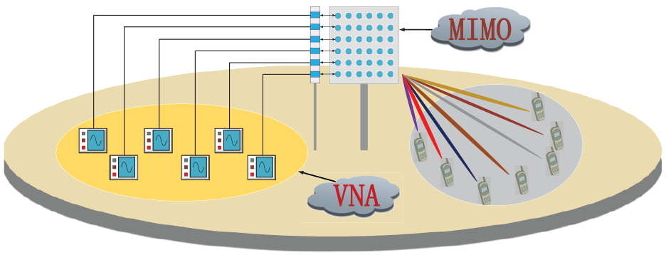
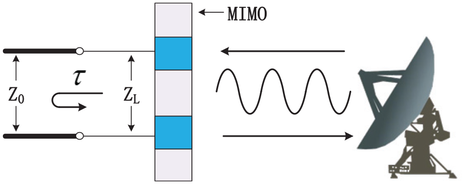
As is shown in Figure 1, 5G signals have the characteristics of severe attenuation and narrow beams and provide the IoT service to distinct users. As a consequence, the deployment of base stations is denser and larger than 4G base stations. For instance, bus stops, office corridors, and street lights are seemingly equipped with 5G base stations. Besides, there are many array elements in 5G massive MIMO, up to 256 × 256. The matching and transmission circuit also tends to be dense, consumes a large amount of energy, and easily accumulates heat. Microwave devices, such as connectors and transmission lines, are sensitive to temperature and are prone to mismatch with antennas. This brings great inconvenience to the measurement. The traditional measurement method is to test the single MIMO element S parameter one by one to ensure whether elements match well with the transmission lines by using VNA, as shown in Figure 2. However, this measurement method is unacceptable under the condition that MIMO contains up to 256 × 256 for the reason that it costs much time. In this article, based on the above scenario, a new measurement method based on microwave imaging is proposed in Figure 3. The MIMO is the device under test (DUT), and it is connected with the matching circuit and transmission lines. The radar is the antenna that transmits the plane wave to illuminate the (MIMO) and detect the matching state of the MIMO array elements by the method of microwave imaging.

Application scenario of MIMO in 5G IoT.
Traditional measurement method in MIMO elements.

Proposed measurement method in MIMO elements.
Proposed method
Microwave imaging theory
The basic imaging method is investigated by the previous scholar and shown.27–29 However, some specific interpretations about imaging theory are still needed: Figure 4 demonstrates the 1-D imaging schematic, and the single frequency incident wave

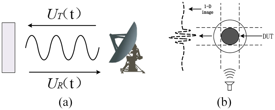
1-D imaging schematic: (a) the side view of 1-D imaging schematic and (b) the top view of 1-D imaging schematic.
The incident signal that irradiates with a time delay and is weighted by the reflection intensity of the received signal
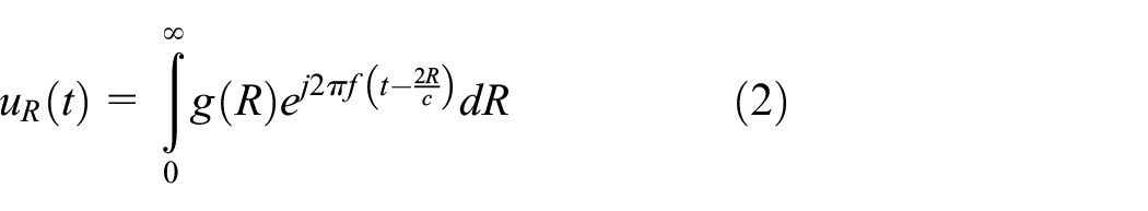
The eventual received signal

According to equation (3), the target reflectance
The 2-D imaging is more intuitive and clear than the 1-D imaging, which is able to display the inverse synthetic aperture radar (ISAR) imaging under the 2-D space with a certain resolution. It is helpful to conduct a multi-dimensional analysis of scattering in engineering. .
The process of microwave 2-D ISAR imaging is shown as follows: 2-D separated processing method is utilized; first, 1-D longitudinal distance resolution of the is obtained, and then the horizontal compression of the aclinic axis is used to obtain the horizontal distance resolution of the aclinic axis. Longitudinal distance resolution of the imaging system is achieved in broadband signal pulse compression, and horizontal distance resolution of the imaging system is achieved in synthetic aperture processing.
The basic geometric relationship of imaging is shown in Figure 5. The transmitting radar antenna is fixed at a certain position and then rotates around the center
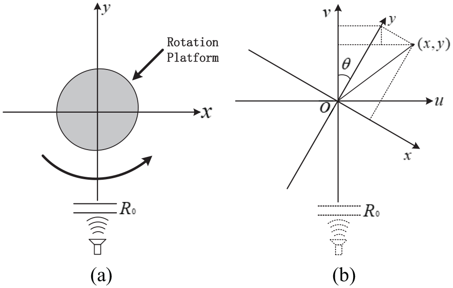
2-D imaging schematic: (a) the top view of 2-D imaging schematic and (b) the basic geometric relationship of 2-D imaging.
According to the conditions described earlier, the signal transmitted by the transmitting radar antenna is a single frequency signal, where the frequency is

The frequency-domain data

According to equation (5), the target reflectance
High-frequency signal transmission model
Transmission line is the device to guide and transmit electromagnetic wave. It is the connection between the transmitting antenna and the transmitter or between the receiving antenna and receiver. According to the traditional theory, high-frequency signals are transmitted on the transmission line from the signal source to the load under the condition that they are in impedance matching state. Otherwise, part of the high-frequency signals will be reflected back to the signal source, resulting in energy loss, as shown in Figure 6.

Transmission line model.
The reflection coefficient


Equation (7) also indicates two extreme conditions when the signal is reflected overall from the load to signal source.
MIMO element scattering model
Antenna is a special kind of measured object. Due to its reciprocity, it is able to both radiate and receive high-frequency electromagnetic signals. According to the antenna scattering characteristic, the scattering of the antenna is divided into two parts: the extra and adjoint item scattering and the mismatched item scattering as shown in equation (8). Total antenna scattering field is demonstrated as the

The first part in the right equation (8) is called the extra and adjoint item scattering or structural item scattering, which has nothing to do with the transmission line circuit but the outer shape. The mismatched scattering is related to the transmission line circuit because the match state between the antenna and the transmission line would determine the reflection coefficient
Measurement schematic diagram.
As is shown in equation (5), the antenna reflectance
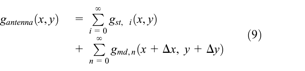
In equation (9),
Simulation
According to the antenna scattering theory, when the element antenna matches well with the transmission line, mismatched scattering is 0 because the energy inputs from the antenna are absorbed by the transmission line and circuits. There is only the extra and adjoint item scattering or structural item scattering left. As a consequence, the scattering model of the matched antenna is replaced by the same dimension perfect electric conductor, which owns the same scattering mechanism as the matched element antenna in the equations (8) and (9). In this section, both the mismatched element physical model and equivalent matched element physical model are constructed in the FEKO software and processing the data from the FEKO in MATLAB. Then their microwave 1-D images and 2-D images are obtained and shown.
MIMO element 1-D imaging verification
The FEKO software is used to construct the MIMO microstrip mismatched element (without connection with matched transmission line or load). Its dimension is 50 mm × 80 mm × 3 mm, which is working at the frequency of 2.4, as shown in Figure 8.
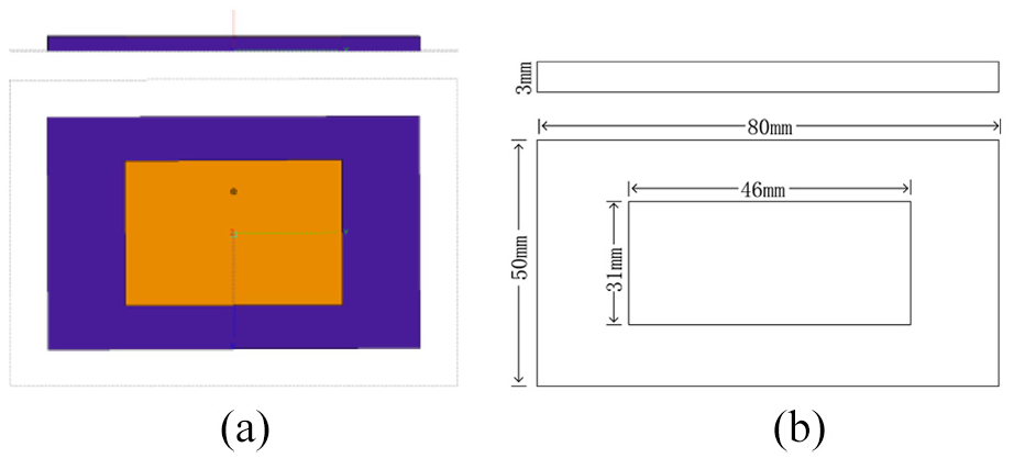
Mismatched element diagram: (a) mismatched element FEKO model and (b) mismatched element dimension diagram.
The equivalent matched element physical model is also constructed in the FEKO software as shown in Figure 9.
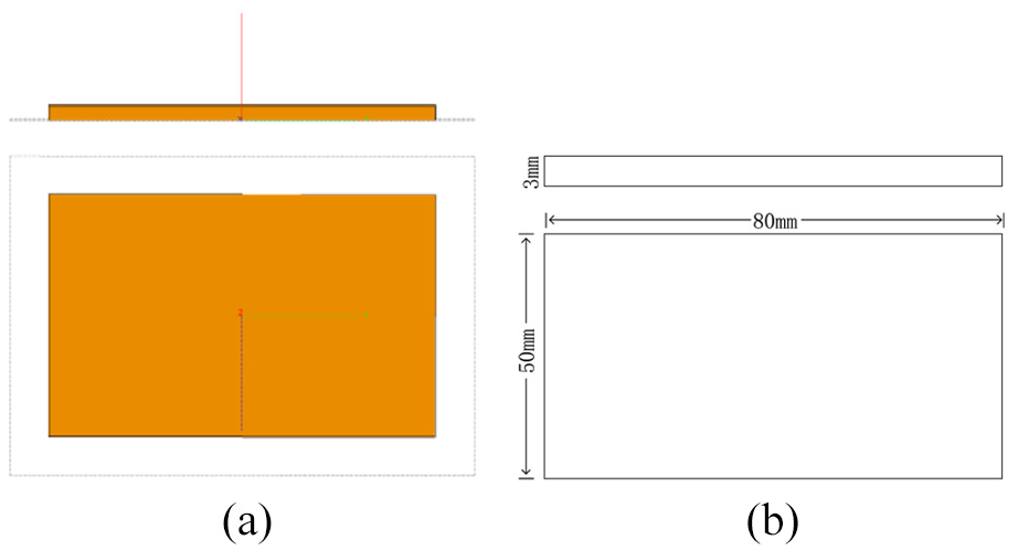
Equivalent matched element model diagram: (a) equivalent matched element model FEKO model and (b) equivalent matched element dimension diagram.
Using the incident plane wave which is vertical to mismatched element and equivalent scattering body plane to irradiate them respectively. The incident direction is as shown in Figure 10.

The incident direction diagram: (a) Incident wave direction of the mismatched element and (b) Incident wave direction of the equivalent matched element.
The incident wave frequency is from 2 to 6 GHz, and its interval is 100 MHz. After obtaining the electronic field data from the FEKO, the data are processed by microwave imaging method in MATLAB and the 1-D microwave imaging of the mismatched element and the equivalent matched element model as shown in Figure 11.

Comparison of mismatched and equivalent matched element 1-D images.
These are two phenomena that are obtained after comparing two 1-D imaging images. First, both the scattering intensity of mismatched element and the scattering intensity of equivalent matched element reach the peak of −25.5 dBsm and −23.5 dBsm at the physical position 0 m on the distance axis, which demonstrates that this is the structural term scattering. Second, the scattering intensity of the mismatched element is 7 dBsm higher than the equivalent matched element from 0.1 m to 0.3 m, which denotes that this is the mismatched term scattering and phenomena also correspond to scattering model. Besides, the difference between the highest peak in both two curves can be explained by the energy conservation law.
However, it is incapable of detecting the match state of the horizontal distributed MIMO when there is more than one element in the same longitudinal distance because the 1-D image will alias together in the same longitudinal distance. The second dimension (horizontal dimension) is needed to detect a distinct match state of elements.
MIMO element 2-D imaging verification
To verify the viability of the proposed method under the 2-D imaging, in this section, a 1 × 2 MIMO that contains a mismatched element and an equivalent matched element is constructed in the FEKO software as shown in Figure 12.

The 1 × 2 MIMO model diagram: (a) top view of the MIMO diagram and (b) side view of the MIMO diagram.
Using the incident plane wave from different angles plane to irradiate the MIMO and the MIMO is always vertical to the incident wave plane. The incident angle
(a) The 2-D imaging incident schematic of 1 × 2 MIMO and (b) 2-D imaging of MIMO.
The 2-D imaging of the MIMO is obtained after processing the data exported from FEKO software in the MATLAB as shown in Figure 13. As shown in Figure 13, there are two strong scattering areas on the mismatched and equivalent matched MIMO element physical positions, respectively. According to the antenna scattering model derived earlier, these two strong scattering images are the structural item scattering. However, there is still another strong scattering area behind the mismatched (left side) antenna, and there is no strong scattering area behind the equivalent matched (right side) antenna model, which corresponds to the mismatched item scattering derived earlier. As a result, the matched antenna and the mismatched antenna in the MIMO are detected by 2-D imaging.
Measurement
In this section, a specific measurement experiment is conducted. The measurement environment is a microwave anechoic chamber, and the experimental equipment includes a VNA, a signal amplifier, a transmitting/receiving antenna, the measured object is a Vivaldi antenna and a 1 m long coaxial cable, and matched/mismatched loads. The experiment first measured the 2-D imaging of the Vivaldi antenna with a matched and a mismatched load to verify the correctness of the method which is capable of detecting the mismatched element in MIMO and then connected the 1 m long coaxial cable with the matched/mismatched load to the Vivaldi antenna for imaging measurement to verify the viability of determining the mismatched location. The expected imaging in mismatched antenna emerges the strong scattering behind the antenna. On the contrary, the expected imaging in the matched antenna presents the weak or void scattering behind the antenna. Particularly, in the 1-D experiment with 1 m long cable and mismatched load, the strong scattering in the physical mismatched position contributes to verify the method feasibility.
Measurement environment and DUT
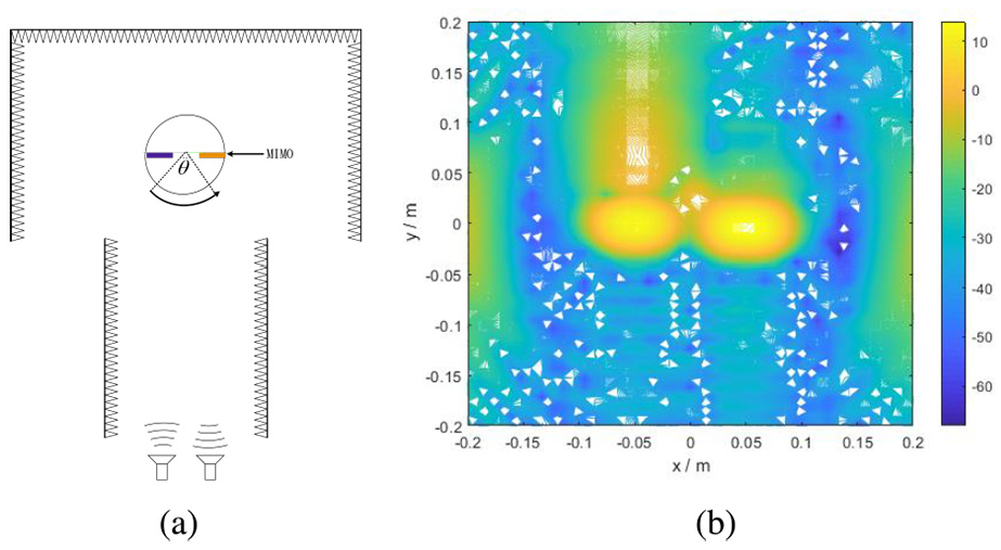
As shown in Figure 14, measurement equipment includes a pair of 2.5–18 GHz transmitting and receiving antennas and a cuboid tunnel to restrict the electromagnetic wave plane dimension, which is shown in (a). An electronic 2-D rotation platform, which is shown in (b). And a VNA in (c). An equipment connection diagram and a specific view of the measurement system are shown in Figures 15 and 16.

Measurement system diagram: (a) transmitting and receiving antenna and cuboid tunnel; (b) 2-D rotation platform; and (c) vector network analyzer (VNA).

Measurement system connection diagram.

(a) Top view of the measurement system and (b) side view of the measurement system.
To correspond with the imaging bandwidth from 2 to 10 GHz, a wide band Vivaldi antenna is designed as the MIMO element (DUT), which is shown in Figure 17. Figure 18 shows its E-plane and H-plane normalized pattern after measured by VNA.

Vivaldi antenna: (a) top view of Vivaldi antenna and (b) backplane of Vivaldi antenna.
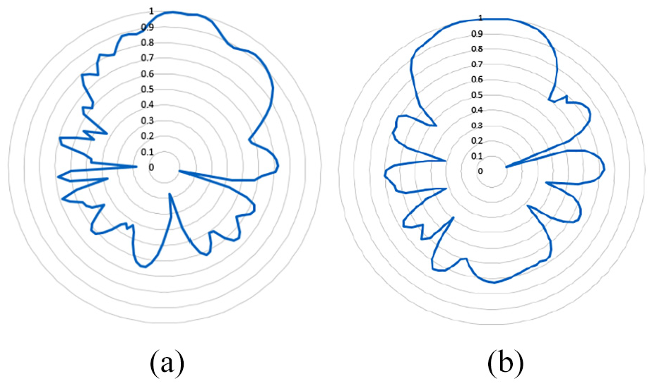
2-D normalized pattern of Vivaldi antenna: (a) E-plane pattern and (b) H-plane pattern.
2-D imaging measurement
To verify the proposed method to detect the MIMO element, a wide band Vivaldi antenna which is placed on the rotation platform aslant is measured under the microwave chamber environment introduced in the part before. Besides, the Vivaldi antenna is connected with the 50 Ω matched load to represent the matched element. Mismatched state element does not connect any load but hang. The measurement scenario diagram is shown in Figure 19, and the specific parameter is shown in Table 1. Note that the 0° sample angle is the circumstance in Figure 19(a), and the anticlockwise direction demonstrates the positive number angle and vice versa.

2-D imaging diagram: (a) top view of diagram and (b) real state of the element.
Element 2-D imaging parameters.

The Vivaldi element under the mismatched and matched conditions on the rotation platform is measured by VNA and the data are processed in the MATLAB software. As a consequence, the 2-D images of the element are shown in Figure 20.

2-D images of element: (a) 2-D images of mismatched element; (b) 2-D images of matched element.
As shown in Figure 20, the measured element is located on the platform whose location is (0, 0). The images in Figure 20 mainly show the 2-D image behind the antenna port position in the longitudinal direction. Observing the two images above, there is a strong scattering area behind the antenna in (a). The reason is that there is a phase difference between the structural item scattering and the mismatched scattering, and the mismatched scattering will occur behind the physical position of the element, resulting in a delayed effect. Compared with Figure 20(a) and (b) scattering still occurs behind the element, but the scattering effect is lower than Figure 20(a). This is because the impedance of the element is not 50 Ω completely but approximately, which is explained by equation (6). The reflected wave in the load still occurs in the 50 Ω load. According to the aforementioned phenomenon, the 1-D mismatched and matched MIMO elements are capable of being detected by the 2-D imaging and the match state of 2-D MIMO elements is also able to be measured following the steps given below: first, measure the MIMO elements in 2-D imaging method one time to ensure the x-axis coordinate of mismatched elements, and then measure the MIMO elements in 2-D imaging method another time after rotating the elements 90° to ensure the y-axis coordinate of mismatched elements.
1-D imaging measurement
After ensuring the mismatched elements utilizing the aforementioned method, the next step is to ensure the mismatched position between the element and the transmission line. To simulate the real circumstance, in this subsection, the element connected with the transmission line and load is constructed. The 1-D imaging is used to detect the accurate mismatched position between the element and the transmission line.
To verify the proposed method to detect the mismatched position, the element connected with the 1 m transmission line, and load is constructed as shown in Figure 21 and the 1-D imaging parameters are shown in Table 2.

1-D imaging diagram: (a) side view of the diagram and (b) real state of the element connected with the transmission line and load.
Element 1-D imaging parameters.
Before measuring the element connected with the transmission line and load, standard sphere measurement is needed to ensure the coordinate of the rotation platform along the y-axis because of the existence of the circuit delay. The 1-D imaging of standard sphere schematic is shown in Figure 22, and the 1-D imaging of standard sphere parameters is the same as the element in Table 2. The 1-D image of the standard sphere is shown in Figure 22(b). According to the image, the highest scattering peak coordinate position is 8.424 m where it is also the platform or DUT coordinate position.

1-D imaging diagram: (a) Side view of diagram and (b) 1-D imaging of standard sphere.
There are two states of element (DUT) in this measurement. The first state is that the element is connected with the 1 m transmission line and open circuit load which means the reflection coefficient

1-D imaging of element.
As is shown in Figure 23, in addition to the strong scattering near the coordinate position of element, the element connected with the transmission line and mismatched load occurs strong scattering area 1 m behind the element position where there is the mismatched load position approximately. However, there is not a strong scattering area on the curve of element with the matched load, which corresponds to the element scattering theory in Proposed method section and the simulation in Simulation section. In this process, the mismatched position of the single element is detected. The 2-D imaging result and 1-D imaging result of the element are concluded in Tables 3 and 4.
Element without 1 m long coaxial line 2-D imaging result.
Element with 1 m long coaxial line 1-D imaging result.

Conclusion
In this research, a measurement method based on the 1-D and 2-D microwave imaging was proposed for MIMO elements. The measurement was demonstrated based on recent work including the theory derivation, FEKO and MATLAB software simulation, and element measurement in the microwave chamber. Compared with the previous studies that primarily measure the total MIMO radiation performance exhibited in the “Introduction” section, this research focused on the detailed scattering mechanism of the element. To solve the mismatching measurement problem, the 1-D and 2-D microwave imaging method is proposed under a dense 5G MIMO elements scenario. The results show that the proposed method is capable of detecting the elements and ensuring the accurate mismatched position of microwave circuits after measuring the elements in 2-D imaging two times and 1-D imaging one time, which improves measurement efficiency. In addition, measurement research under other specific mismatched conditions (such as short circuit mismatched or part mismatched) was not addressed in this research and is a valuable future contribution to this work.
Footnotes
Handling Editor: Bo Rong
Declaration of conflicting interests
The author(s) declared no potential conflicts of interest with respect to the research, authorship, and/or publication of this article.
Funding
The author(s) disclosed receipt of the following financial support for the research, authorship, and/or publication of this article: The work by Tao Hong is supported by National Natural Science Foundation of China under Grant No. 61827901.