
Abstract
This article proposes an intelligent monitoring system for semiconductor manufacturing equipment, which determines spec-in or spec-out for a wafer in process, using Internet of Things–based big data analysis. The proposed system consists of three phases: initialization, learning, and prediction in real time. The initialization sets the weights and the effective steps for all parameters of equipment to be monitored. The learning performs a clustering to assign similar patterns to the same class. The patterns consist of a multiple time-series produced by semiconductor manufacturing equipment and an after clean inspection measured by the corresponding tester. We modify the Line, Buzo, and Gray algorithm for classifying the time-series patterns. The modified Line, Buzo, and Gray algorithm outputs a reference model for every cluster. The prediction compares a time-series entered in real time with the reference model using statistical dynamic time warping to find the best matched pattern and then calculates a predicted after clean inspection by combining the measured after clean inspection, the dissimilarity, and the weights. Finally, it determines spec-in or spec-out for the wafer. We will present experimental results that show how the proposed system is applied on the data acquired from semiconductor etching equipment.
Introduction
The Internet of Things (IoT) is an evolution of future Internet in which things will become smarter and actively communicate with other things. The IoT technology enables the interconnection between large volumes of distributed and heterogeneous smart things allowing them to communicate seamlessly with the user. The rapid advancement and ubiquitous penetration of IoT devices will accelerate innovations in a variety of industries such as healthcare, automotive, surveillance, semiconductor, energy, retail, and smart city.1–6 Among these, intelligently monitoring the process of manufacturing semiconductors is one of the very significant topics.7–10
The semiconductor chip could be considered the greatest invention of the 20th century. Since their initial invention, semiconductor chips are currently used in nearly all products, including not only computers but also various home appliances. Semiconductor manufacturing processes became more complex over the decades due to the continuous needs for smaller and higher density chips. For a single silicon wafer to become semiconductor chips, it undergoes hundreds of processes over the course of 4–10 weeks. In addition, the sequence is not linear; several major processes must be repeatedly performed.
A FAB (fabrication facility) is dually composed of both manufacturing equipment and testing devices. A testing device requires a longer operating time than the manufacturing equipment, and the manufacturing equipment must be stopped for testing a wafer. For this reason, the testing process reduces the utilization rate of a FAB. To improve the rate, sample tests are performed in most cases. A sample test cannot detect faults that occur in the process. The faults are detected in the final inspection stage. If a fault is detected in that stage, the lot of wafers including the fault is disposed of. To improve the yield rate, the advancement in semiconductor manufacturing technology increases the demand for a higher level monitoring system for the manufacturing process control.11,12
Semiconductor manufacturing equipment consists of a few hundred built-in sensors for monitoring the tool status and the process. Sensory data are full of useful information about the equipment status and the corresponding process and can be utilized for the detection of an incipient fault on a wafer-in-process. However, the handling of a large amount of equipment data is arduous. The existing monitoring systems for semiconductor manufacturing equipment can be classified by three approaches: real-time measurement,13,14 model-based prediction,15–19 and pattern recognition.20–23
The first approach is very traditional. We already mentioned the overview and the drawbacks of the approach in the previous paragraph. The second approach is implemented by expressing the relationship between the parameters of manufacturing equipment and the measurement value as a function and then predicting the measurement value based on the input time-series. The problem with this approach is the difficulty of expressing the relationship between two parameters in terms of a precise function. The third approach learns a pattern recognition model, such as an artificial neural network (ANN), using the previously collected measurement values and the corresponding status data of manufacturing equipment, and then compares the input status data and the learned status data to the output measurement values corresponding to the most similar status data. There are three famous techniques in this approach, using k-NN (k-nearest neighbor), 19 ANN,20–22 and Bayesian network 23 as the recognition model. Because all three of these are systems that monitor whether a specific parameter value exceeds the pre-defined range, one shortcoming is their inability to predict the final ACI (after clean inspection) that is formed by all of the parameters.
In this article, we propose an intelligent real-time monitoring system that decides spec-in or spec-out for a wafer from a predicted ACI in real time. The predicted ACI is calculated by integrating all parameters of a specific piece of manufacturing equipment. Figure 1 is an overview of the proposed system that consists of three modules: initialization, learning, and prediction.

Overview of the proposed system.
“Initialization” is a module to initialize the system for manufacturing equipment to be monitored. It performs the function of reading the learned data from files, setting the level of importance and effective steps of the parameters that belong to manufacturing equipment, and inputting the threshold values. “Learning” is a module that performs clustering for every parameter using the LBG (Line, Buzo, and Gray)24–26 algorithm. To predict an ACI, it is necessary to calculate the similarity between the clustered time-series pattern and the input pattern. The proposed system uses DBA (DTW barycenter averaging) based on DTW (dynamic time warping)20,27 to find the cluster’s average pattern and SDTW (Statistical DTW)28,29 to calculate the similarity between the clustered time-series pattern and the input pattern. “Prediction” is a module that calculates a predicted ACI using SDTW. Finally, the system decides spec-in or spec-out for a wafer from a predicted ACI in real time.
The remainder of this article is organized as follows. Section “Initialization of the monitoring system” describes initialization. Section “DTW and SDTW” explains the DTW and SDTW to calculate the dissimilarity between two time-series. Section “Clustering and ACI prediction” explains the clustering algorithm using the revised LBG and how to calculate a predicted ACI. In section “Experimental results,” we present several experimental results, and conclusions are presented in section “Conclusion.”
Initialization of the monitoring system
Initialization consists of two functions: the effective range and weight setup, and the weight optimization. The first task in this phase is to input the number of the recipe that indicates the type of process that will be monitored. Therefore, the input data in the phase are the process type number, the effective ranges, and the parameter data.
The process type number is a code number used to identify a particular process that is distinct from the numerous other processes involved in the manufacturing of semiconductors. The effective range is a time-series of significant data that affects the processing results among the processing steps. The parameter data consists of the number of parameters to be applied by the monitoring system, as well as the weight of each parameter. Before explaining the method of setting up the effective range and adjusting the weights, to facilitate the understanding of the monitoring system described in this article, we will first explain the wafer’s data structure which needs to be inputted.
The data structure for the wafer used in this article is as shown in Figure 2. We call it a wafer data structure (WDS). In Figure 2, invalid data refers to the status data that corresponds to the beginning and end of each step during the transition between steps. Because, at the beginning and end of each step, there is a high probability of noise which does not affect the actual process, the data with this noise is excluded from processing by the monitoring system to ensure an accurate prediction. The range of valid data is determined by the operator’s experience.

Wafer data structure.
The initial weights for all parameters are determined as follows. First, the operator inputs a relative importance for each parameter as a numerical value. For example, let us attempt to classify the importance into three levels. The operator inputs 3 for the most important parameter, 2 for the lesser, and 1 for the lowest. After setting up the weights for all parameters, we recalculate the weights using equation (1)

In equation (1), n is the number of parameters for which the importance has been established, and L(i) is the importance of the ith parameter. By equation (1), the weights are normalized between 0 and 1.
DTW and SDTW
In this article, we use DTW to align the entered data and to calculate the dissimilarity between two time-series for clustering multiple time-series patterns and SDTW to calculate the dissimilarity between a time-series and a reference model.30,31
In DTW, dissimilarity is calculated by comparing a test signal t = |t1, t2, …, tN| with a stored reference signal r = |r1, r2, …, rN| by means of dynamic programming

In SDTW, the reference R = [R1, R2, …, RNR] is not a signal but a statistical model consisting of a normal distribution for each time point j with mean μj, covariance matrix Σ j , and transition probability αj(Δϕ): Rj = {μj, Σ j , αj(Δϕ)}. Δϕ∈P is a transition of the warping path to a point with state j, where P are the possible transitions from (ϕt(j − 1), ϕR(j − 1)) to (ϕt(j), ϕR(j)). The dissimilarity CΦ(t, R) is defined by


where Φ = {ϕt(1), …, ϕt(N∅), ϕΦ}, ω(P(n)) is a function that assigns a weight to a transition type, and C*(t, R) is the final dissimilarity. Under the three constraints of DTW, the warping path starts in Φ(1) = (1,1) and ends in Φ(NΦ) = (Nt, NR), and the set of possible transitions is P(n) = ⌊(ϕt (n+1) − ϕt(n)), (ϕR(n+1) −ϕR(n))⌋∈[0,1], [1,0], [1,1]. The distance function is defined as the following
Because SDTW is implemented by dynamic programming, the recursive properties represented in a bottom-up approach are easier to understand and implement. This article rewrites equation (4) as

To obtain the final result from equation (6), SDTW calculates the dissimilarities for all of the elements of the two-dimensional corresponding table composed of C(1,1) to C(Nt, NR).
Clustering and ACI prediction
In the prediction phase, we first retrieve the best matched data set, which has the smallest dissimilarity, from the collected data sets for learning by comparing an input data set with the collected data sets, and then extract the ACI of the best matched data set; finally, we calculate a predicted ACI using the extracted ACI and the dissimilarity. At this time, the time-consuming problem can occur to retrieve the best matched data set from a great deal of learning data sets. Therefore, it is necessary to perform clustering,32–34 in which time-series patterns that have similar characteristics are grouped together, and the representative for that group is selected. To perform clustering, we use the LBG algorithm.
The processing of the LBG algorithm is similar to that of the K-means. The difference lies in the method used to select the representative of the cluster. In the K-means, the representative is the average of the patterns that comprise the cluster, while in LBG, the cluster’s representative is the pattern that minimizes the average distance to the patterns included in the cluster. The purpose of this article is not to output ordinary pattern recognition, that is, not to output the identifier for the pattern with the greatest similarity among the learning data, but rather to output the ACI of the pattern and the dissimilarity. Therefore, it is also necessary to average the ACIs because of the averaging of the data sets included in the cluster. This approach is based on the premise that similar time-series patterns will also have similar ACIs. Unfortunately, the patterns handled in this article do not necessarily have similar ACIs even if their forms are similar. Therefore, we must calculate the cluster’s representative using a method that will not transform the given data if at all possible. For this reason, to perform clustering in this article, we used an algorithm that is a slightly modified version of LBG, as shown in Figure 3.

Modified LBG algorithm.
Manufacturing equipment discretely generates state data for all parameters every second while it is processing a wafer. We refer to these data as wafer state data. The clustering for the numerous wafer state data is independently performed for every parameter. Therefore, the modified LBG algorithm is independently applied to each parameter.
The prediction module includes the process of retrieving the most similar state on the collected data sets for learning with an input wafer state. However, because the clustering is performed independently for every parameter, a problem occurs. That is, the retrieved states for an input wafer are not for a wafer but multiple wafers because the prediction module finds the most similar state for every parameter. To overcome this problem, this article expresses the wafer state data used in the learning stage in terms of the cluster’s number of every parameter, as shown in the equation (7)

To determine spec-in or spec-out of a wafer in the process based on the input state data in real time, we first calculate a predicted ACI by referring the learning data as follows. This article first expresses the input state data as a code sequence, such as equation (7), and then calculates a predicted ACI using the equation (8). The code sequence consists of the cluster number of every parameter. The cluster number of a parameter is selected by SDTW with the input state and reference model
In equation (8), IV denotes the ACI of the best matched pattern, and D(i) and W(i) denote the dissimilarity and weight for the ith parameter, respectively.
Experimental results
Data for experiments are obtained from an etching machine, which is a semiconductor manufacturing device, and ACI values are obtained from the corresponding measurement device. The etching machine is already installed in the production line of a fabrication facility and the machine performs reactive ion etching. The proposed system uses time-series data for all parameters and an ACI in the learning stage, but only time-series data in the prediction stage. The output value of the prediction is the ACI for an etching process. There are 15 sets of data used for learning. Each data set consists of eight stages for 18 parameters, respectively. The valid range for each parameter is set by an experienced operator in the initialization phase.
To evaluate the performance of the proposed system, we investigate how to change the difference between the measured ACI and the predicted ACI for seven test sets. Furthermore, we evaluate the impacts for the five major parameters, the weights of the parameters, and the two major steps.
First, we examine the difference between the predicted ACI and the measured ACI according to the number of learning. Table 1 shows the differences for three sets (F6735X, F674EX, F791PX) among the seven test sets (F6735X, F674EX, F681YX, F70QAX, F791PX, F791TX, F796UX). Figure 4 visually presents the differences for all seven test sets. From Figure 4, we notice that the differences decrease according to increasing the number of learning for all seven test sets.
Difference between actual and predicted ACI values.

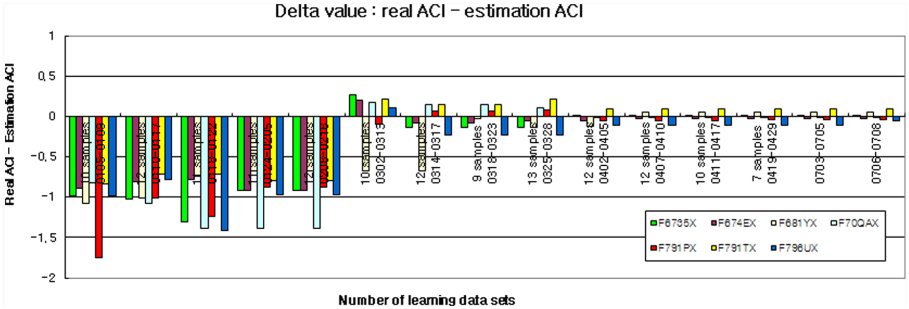
Difference between actual ACI and predicted ACI values.
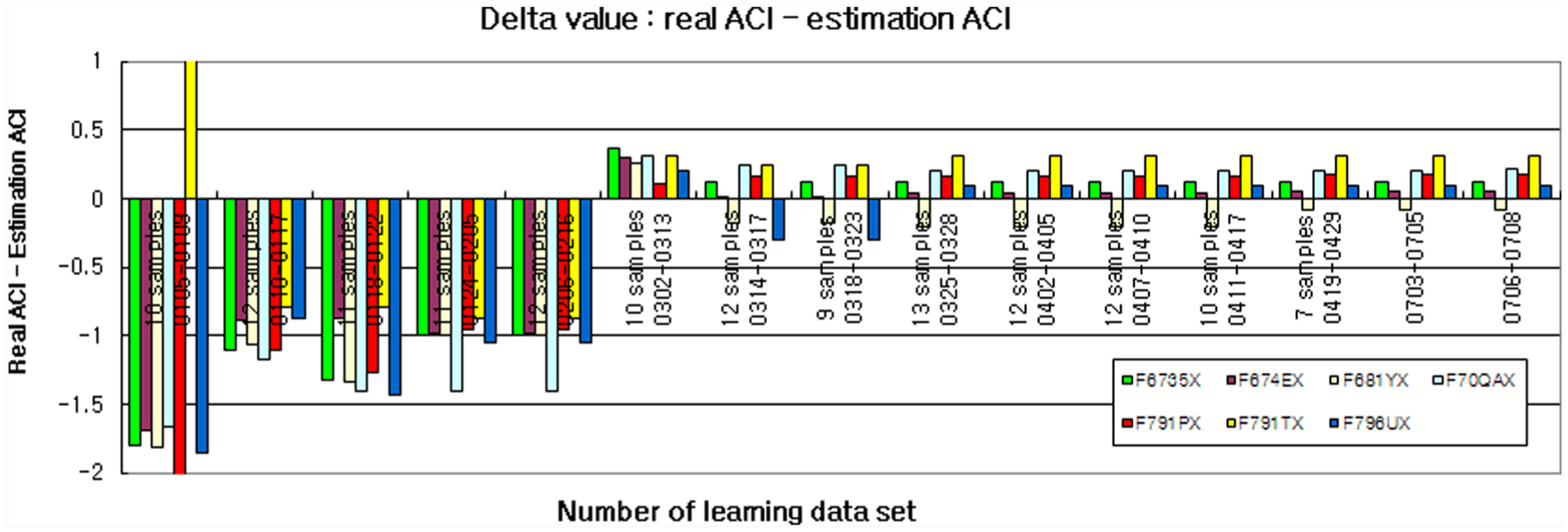
Second, we investigate the impact for the major parameters given by the experienced operators. We also find that the differences decrease according to increasing the number of learning for all seven test sets, as shown in Figure 5. From these experimental results, we confirm that the heuristic knowledge of the operators is effective but less accurate.

Evaluation using only the major parameters.
Next, we randomly reset all weights of parameters to probe the impact for the priorities of the parameters. There are cases in which the error value increases even as the amount of learning increases in Figure 6. From these results, we recognize that Figure 6 demonstrates that it is very important for an operator to set weights of parameters suitably in the initial phase.
Evaluation with a change in the data on the weighted level of importance.
Finally, we evaluate the impact of the third and fourth major steps. The results indicate that the accuracy improved to some degree as the amount of learning increased, but is not acceptable. The poor accuracy is caused by setting the third and fourth for all parameters as the major steps. Therefore, we can see that the effective steps for a parameter are set more elaborately.
It is important to initialize the weights (relative importance) of the parameters during the monitoring process. The operator inputs a relative importance for each parameter as a numerical value, which is recommended by the new monitoring system. After setting up the initial weights for all parameters, the weights are normalized. Usually, traditional systems tend to initialize all equipment concerning manufacturing processes with same parameters, so that the systems cannot reflect the characteristics of the equipment sufficiently. However, the new monitoring system initializes the weights differently considering the characteristic of equipment. In addition, the suggested system tries to minimize the inaccuracy due to inadequate setting of weights through the weight training process. Anyhow, the results of both traditional and new systems can be dependent on the initial weights.
In this article, sensor data are generated in real time from seven different semiconductor manufacturing equipment sensors and one tester sensor. In other words, sensor data are consecutively generated from a total of eight sensors, which are sampled once per second (1 Hz). Accordingly, eight sensor data per second are generated, 28,800 sensor data are generated in 1 hour, and 691,200 sensor data are generated in 1 day. Then, about 20,736,000 sensor data are generated in 1 month, and 248,832,000 data are generated in 1 year. In the suggested system, the sampling rate for acquiring data from each device is designed to be adjustable. Therefore, if the sampling rate is adjusted, the number of generated data also changes.
In terms of space for storing data, storage space is required in proportion to the number of generated sensor data. If the sampling rate of the data generated from semiconductor manufacturing equipment sensors and the tester sensor is different from each other, the average is taken to synchronize the data. For example, suppose that the sampling rate of the data generated from the manufacturing equipment sensor is 2 Hz and the sampling rate of the data generated from the tester sensor is 1 Hz. Then, the average of the data can be used to synchronize the data generated from the manufacturing equipment with the sensing data generated from the tester.
Conclusion
This article proposed an intelligent monitoring system of semiconductor manufacturing equipment using big data analysis and presented experimental results using the wafer state data sets obtained from an etching machine. The conclusions obtained from the experimental results are as follows. We confirmed that the effective steps and the weights of parameters are properly set in the initialization phase, using a greater number of data for the learning produces more accurate results, and the used clustering algorithm is adequate to retrieve the best data set from the learning data sets successfully.
Future works will include setting the effective steps and the weights of parameter automatically and more accurately because the manual work is very tedious and error-prone, as well as applying them to other semiconductor manufacturing equipment.
Footnotes
Academic Editor: Paolo Bellavista
Declaration of conflicting interests
The author(s) declared no potential conflicts of interest with respect to the research, authorship, and/or publication of this article.
Funding
The author(s) received no financial support for the research, authorship, and/or publication of this article.