
Abstract
With the rapid development of embroidered electronics, the research on microstrip lines as important connecting devices is crucial. Although the proposed research has explored the influence of embroidery parameters on some electrical properties of embroidered electronics, it is difficult to design and fabricate embroidered microstrip lines (EMLs) with specific transmission performance based on existing research. Therefore, in order to better design and fabricate EMLs with good transmission performance, the effect of embroidery parameters on their transmission performance needs further exploration. In this work, relevant models to simulate their transmission performance was proposed. Firstly, considering the cases where the conductive yarn is only distributed on the fabric surface as well as in both the surface and the thickness direction of the fabric, two geometry models are constructed to simulate the path of the conductive yarn in the embroidered conductor strip. Based on this, the transmission performances of the EML are simulated and analyzed. Then, two different sets of embroidered conductor strips were manufactured to fabricate microstrip line, and their transmission performance was tested to verify the rationality and accuracy of the above simulation model. Finally, based on simulation analysis and experimental testing, the influence of stitch spacing and stitch length on the transmission performance of EMLs are investigated, and the prediction bias of the models is analyzed. It is believed that the proposed model will provide a theoretical basis for the design of EMLs.
Introduction
Recently, wearable electronics are emerging rapidly in security, healthcare, and biomedical application.1–3 As the essential components of many wearable electronics, microstrip lines play a role in transmitting signals. Furthermore, the characteristic impedance of designed microstrip line is required to match its connecting components well and it should has good transmission performance. 4 And, the insertion loss is an important parameter for the signal transmission efficiency of microstrip lines. 5 For the wearable EML, the embroidery parameters determine the distribution of conductive yarns and improper fabrication parameter settings could result in the nonconformity of the conductive tracks and damage the conductive coating of the conductive yarns, and further affect its electrical properties. 6 Therefore, in order to design and fabricate EMLs with good transmission performance, it is crucial to explore the influence of embroidery parameters on their transmission performance.
The relevant research on the influence of embroidery parameters on electronics were conducted. Seager et al.
7
investigated the effect of stitch direction on the performance of embroidered patch antennas, and pointed out that the stitch direction could influence its
In order to better design and prepare embroidered electronics, scholars have proposed some models to simulate their performances. Based on traditional electronic models, some scholars have proposed that the embroidered conductive parts are considered as uniform conductors.7,9,10 Ouyang et al.
9
designed a test setup and applied a high-Q waveguide cavity based measurement technique to obtain an equivalent solid surface conductivity. The high-Q waveguide cavity could measure the load Q and
In this study, the effect of embroidery parameters on the transmission performance of EMLs are investigated by simulation and measurement. Two geometry models were proposed to simulate the structure of conductor strip, and the performance of EMLs were obtained. Moreover, the EMLs with different parameters were fabricated and their transmission performance was measured. Combined the measured and simulated results, the better model was determined. The research is beneficial for the design and preparation of EMLs with good transmission performance, providing theoretical basis for the design and preparation of embroidered electronics.
Design of fabric-based embroidered microstrip lines
The structure of microstrip line is shown in Figure 1, it consists of the conductor strip, substrate and ground plate. In order to obtain the microstrip line with a certain characteristic impedance, conductor strips must be designed according to the dielectric constant and thickness of substrate. The structure schematic of microstrip line.
In order to apply the microstrip line to common electronic devices, the characteristic impedance of the microstrip line designed in this work is 50 Ω. According to the thickness h and the dielectric constant

Among


According to the published work, cotton, nonwoven fabric and felt were the common textile materials for their low dielectric loss, low cost, light weight, etc. 13 Furthermore, the nonwoven fabric had very low dielectric loss, and it was very soft and easy to embroider. In this work, considering the design of conductor strip, the multilayer polyester nonwoven fabric sewed by 40s/3 polyester sewing thread was used as substrate. The polyester sewing thread was obtained from Ningbo Guman Textile Co., Ltd. (Yinzhou, China). The single-layer polyester nonwoven fabric with a mass per unite area of 79 g/m2 was used to fabricate the conductor strip, and purchased from Shandong Jiantong Eng. Tech. Co., Ltd. (Dezhou, China). Its single-layer thickness is 0.716 ± 0.018 mm according to GB/T3820-1997 standard (Determination of thickness of textiles and textile products) by fabric thickness gauge (YG141 N, China). Its dielectric constants and dielectric losses tangent are 1.134 and 0.00137, respectively, measured by IPC TM 2.5.5.13 (Relative Permittivity and Loss Tangent Using a Split-Cylinder Resonator) test standard. The silver-plated nylon multifilament yarns were used as the top and bottom line for embroidering conductor strip into the nonwoven fabric. It was purchased from Qingdao Hengtong X-silver Specialty Textile Co., Ltd. (Qingdao, China). The copper fixture was used to present the ground plate. According to the study, 14 the fabric embroidered only with conductive yarns is not a part of the equivalent substrate. Thus, the additional two-layer nonwoven fabrics without conductive yarns were used as substrate in this work. From equations (1)–(3), the width of microstrip line is calculated as 6.394 mm, and used as 6.40 mm for the limitation of production accuracy. Based on the theory of microstrip line, 5 its length having no influence on the characteristic impedance of the microstrip line was set as 52.00 mm.
Simulation of fabric-based embroidered microstrip lines
In this work, high frequency structure simulator (HFSS) software was used to simulate transmission performance of the EML. For the conventional microstrip line, its structures, shown in Figure 1, material properties and boundary conditions need to be built in the simulation by HFSS. Its conductor strip and the ground plate are usually made of solid copper foils, and its substrate is PCB board. In the EMLs, its conductor strip consists of conductive yarns and substrate is fabric, and the relative geometry structure and properties should be proposed to simulate its structure and materials. In addition, the boundary conditions also should be set according to its properties.
Geometry model of embroidered microstrip line
In this part, two kinds of geometry models were proposed to simulate the distribution of conductive yarns in the fabric. Based on the simplified model, 7 the distribution of conductive yarns only on the fabric surface was considered, the geometry model referred as surface conductor strip was established. The structure formed by surface conductor strip, substrate as well as the ground plate is called “surface microstrip lines”. In addition, according to the actual path of the conductive yarn (including the distribution of conductive yarns in both the surface and thickness direction of fabrics), the geometry model referred as three-dimensional conductor strip was established. Similarly, the structure formed by three-dimensional conductor strip, substrate as well as the ground plate is called “three-dimensional microstrip lines”.
According to section 2, the width and length of the conductor strip were 6.40 mm and 52.00 mm, respectively. The following model of embroidered conductor strip was set with the stitch spacing 0.80 mm and the length 4.00 mm.
Geometry model of surface microstrip line
The model of surface microstrip line, including its structures and boundary conditions, is shown in Figure 2(a). Figures (b) and (c) were the top and front view of embroidered microstrip line. According to the actual structure, the embroidered conductor strip is composed of many parallel conductive yarns along the length direction and enclosed at both ends. Considering that using a cylindrical structure to simulate the conductive yarn can result in excessive computational complexity and even inability to obtain simulation results.
15
Thus, the uniform cuboids were used to simulate the conductive yarn instead of the cylindrical structure. The length and width of the uniform cuboid were set as 52.00 mm (the length of the conductor strip) and 0.16 ± 0.01 mm (the diameter of the conductive yarn), respectively. In the model of surface microstrip line, according to the effect of skin effect,
16
the current will concentrate on the surface of the conductive yarn and the effective thickness of the silver-plated conductive yarn is twice the thickness of the silver plating layer (2.38 ± 0.01 μm). Therefore, the cuboids with above effective thickness ( 4.76 ± 0.20 μm) could be used to simulate the structure of conductive yarn.7,11 (a) The surface simulation model; (b) top view; (c) front view of embroidered microstrp line.
For the substrate, it was simulated as uniform cuboids with dielectric constants of 1.134 and dielectric losses tangent of 0.00137. Its width and length are 100.00 mm, and 52.00 mm, respectively. The thickness was set as the thickness of double-layer nonwoven fabrics. In addition, the copper plate was simulated as uniform cuboids. Its length and width are the same as those of the substrate, and its thickness was 5.00 mm. Then, the cuboid was established to present the air radiation. Its bottom structure was coincided with the bottom structure of the copper plate, and the distance between its top structure and the top structure of substrate was slightly greater than
Geometry model of three-dimensional microstrip line
The model of three-dimensional microstrip line, including its structures and boundary conditions, is shown in Figure 3(a). Figures (b) and (c) were the top and front view of embroidered microstrip line. Similarly, the embroidered conductor strip is composed of many parallel conductive yarns along the length and thickness direction, and the conductive yarns enclosed at both ends. In this model, uniform cuboid with the length 52.00 mm, the width 0.16 ± 0.01 mm and the thickness 2.38 ± 0.10 μm (the effective thickness of conductive yarn) was used to present the conductive yarns. The remaining structures are the same as the geometry model of the surface microstrip line. (a) Three-dimensional simulation model; (b) top view; (c) front view of embroidered microstrp line.
Material properties and boundary conditions setting
Material properties
Two-layer nonwoven fabrics were used as substrate, and were set to be isotropic materials with the dielectric constants of 1.134 and losses tangent of 0.00137. The conductor strip is formed by many top and bottom conductive yarns. The conductive yarn is silver-plated nylon multifilament, consisting of 36 filaments. The surface morphology and cross-section of each filament are shown in Figure 4. From Figure 4(a), the diameter of filament is 20.29 ± 0.18 μm. As shown in Figure 4(b), the silver-plated thickness of each filament is 1.19 ± 0.05 μm. According to the calculation formula,17,18 the silver-plated cross-sectional area of each filament is 71.41 μm2, and the total silver-plated cross-sectional area of each conductive yarn is 2570.76 μm2. The resistance of conductive yarn is 422 SEM image of silver-plated filaments: (a) surface morphology; (b) cross section.

According to equation (4), the resistivity of the conductive yarn is 1.08 × 10⁻⁶ Ω•m, and its conductivity is 9.26 × 10⁵ S/m. In addition, the conductivity of the copper plate with the thickness 5.00 mm is 2.7 × 10⁷ S/m.
Boundary conditions setting
Set the air radiation boundary as radiation and both ports as wave ports. The conductor strip and copper plate were both set as finite conductivity, its parameters were set according to the properties of conductive yarn and copper plate. The convergence coefficient was set to the default of 0.02 to reduce the number of grid divisions and computational complexity in the simulation.
Simulation analysis of embroidered microstrip line
Current distribution
According to the simulation models of the surface and three-dimensional microstrip lines, the current distribution of the EML with 0.8 mm stitch spacing and 4 mm stitch length is shown in Figure 5. By comparing their current distributions in figures (a), (b), and (c), it can be observed that the current in the microstrip line not only flows along the conductive yarn on the fabric surface, but also along the conductive yarn in the thickness direction of fabric. The phenomenon is consistent with the flow pattern of current at low frequencies.
7
Surface and longitudinal cross-sectional currents distribution of conductor strips for EMLs with different geometry model: (a) surface microstrip line; (b) three-dimensional microstrip line(surface);(c) three-dimensional microstrip line (longitudinal cross-sectional).
Transmission performances
The insertion loss of EML simulated by surface and three-dimensional microstrip lines model were shown in Figure 6(a) and (c). Their simulated results both show that the insertion loss The simulated insertion loss 
Using one-way analysis of variance with a confidence interval of 95%, the insertion loss and transmission coefficient of EML simulated by the two models were compared. The probability p-values (p < .00, p < .00) were both less than 0.05, indicating that the insertion loss and transmission coefficient simulated by the two models both have a significant difference. It suggests that the conductive yarns in the thickness direction have a significant impact on the transmission performance of EMLs. Therefore, the three-dimensional microstrip line model can more accurately simulate the performance of the actual EMLs.
Experimental section
Preparation of embroidered microstrip line based on fabric
The process of microstrip line embroidered by satin stitch was shown in Figure 7. First, the width of the conductor strip was calculated by equations (1) to (3) and its length was set to 52 mm, and their sizes were set through the embroidery software. Then, the conductor strip is embroidered on the nonwoven fabric by a computerized embroidery machine (brother NV 950, Brothers (China) Commercial Co., Ltd.). Next, the fabric embroidered with the conductor strip and the extra nonwoven fabrics were sewed together with the polyester sewing threads by the embroidery machine. Finally, the nonwoven fabric with the conductor strip was placed directly on the copper plate fixture to form a complete microstrip line. The formation of embroidered microstrip line.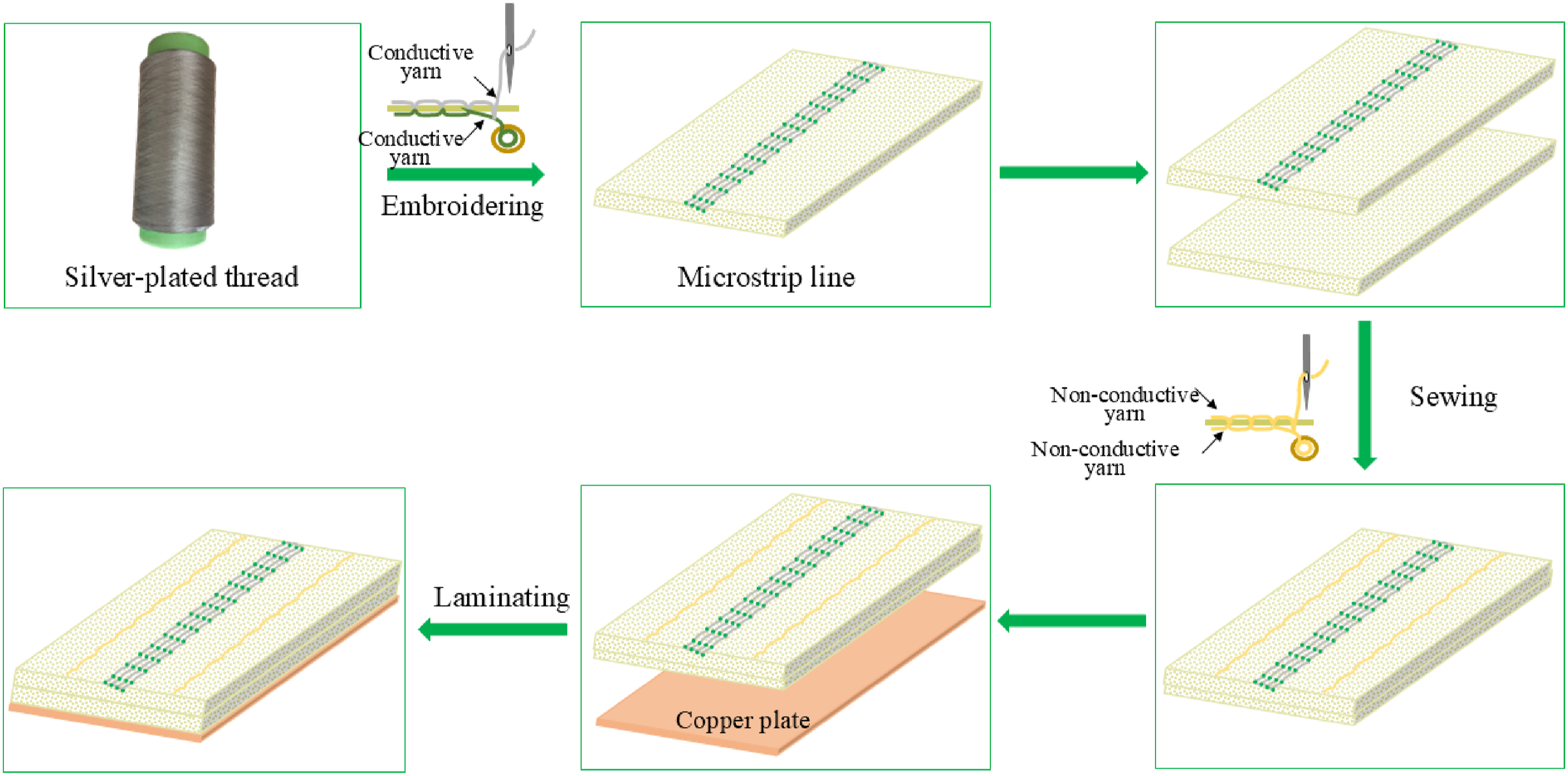
In order to verify the feasibility of above simulation model, two sets of embroidered conductor strips with different parameters were fabricated to form EMLs. The first group conductor strips have a fixed stitch length of 4.00 mm and its stitch spacings were set as 0.20 mm∼2.00 mm and gradient were 0.60 mm. The second group conductor strips have a fixed stitch spacing of 0.4 mm and its stitch lengths were set as 1.60 mm∼6.40 mm, and gradient were 1.60 mm.
Measurement of embroidered microstrip line based on fabric
To demonstrate the electromagnetic performance, the transmission properties of microstrip line were measured using a vector network analyzer VNA (Agilent E5071 C) as shown in Figure 8. The embroidered conductor strip was placed on the fixture and its two ends were contacted with the two parts of the SMA connectors, respectively. Then, a coaxial cable with 50 Ω were used to connect SMA connector. The vector network could measure its transmission properties. Each sample was tested three times and their average value was taken. The test schematic diagram of the transmission performance of EML
Results and discussion
The effect of stitch spacing on the transmission performance of embroidered microstrip line
The measured and simulated performances of the EMLs with different stitch spacings were shown in Figure 9. The measured and simulated The performance of the EMLs with different stitch spacings: (a) the measured and simulated 
Using one-way analysis of variance with a confidence interval of 95%, the measured insertion loss and transmission coefficient of EMLs were compared. The probability p-values (p < .00, p < .00) were both less than 0.05, indicating that the stitch spacing has a significant impact on the transmission performance of EMLs. As mentioned before, for the EMLs with different stitch spacings, their insertion loss depends on the conductor loss of embroidered conductor strip. As the stitch spacing increases, the resistance of conductor strip increases 20 and its conductivity decreases gradually. Among then, the conductivity of conductor strip with 0.20 mm stitch spacing is largest so its conductor loss is lowest. For the conductor strip with 1.40 mm and 2.00 mm stitch spacing, they have similar conductivity, resulted in similar conductor loss. In addition, it can be observed from figures (b) and (d) that the transmission coefficients of EMLs with different stitch spacing are all above 0.92, indicating that their transmission performances are good.
In order to compare the deviation between measured and simulated results, their error rates were calculated and shown in Figure 10. It can be observed that the error rate resulted by the three-dimensional microstrip line model is smaller than that of the surface microstrip line model, indicating that the former results are closer to the actual test values. At the same time, it indicates that the conductive yarn in the fabric thickness direction affects the transmission performance of the microstrip line. In addition, the maximum error rate obtained by surface microstrip line model is 5.78%, that of three-dimensional microstrip line model is 4.85%. Therefore, both surface and three-dimensional microstrip line model can predict the insertion loss and transmission coefficient of EMLs, and the latter are more accurate. The deviation rate between the measured and simulated transmission coefficients of EMLs with different stitch spacings.
The effect of stitch length on the transmission performance of embroidered microstrip line
The measured and simulated performances of the EMLs with different stitch lengths were shown in Figure 11. The measured and simulated The performance of the EMLs with different stitch lengths: (a) the measured and simulated 
Similarly, one-way analysis of variance with a confidence interval of 95%, was used to compare insertion loss and transmission coefficient of EMLs. The probability p-values (p < .00, p < .00) were both less than 0.05, indicating that the stitch length has a significant impact on its transmission performance. As mentioned before, for the EMLs with different stitch lengths, their insertion loss depends on the conductor loss of embroidered conductor strip. As the stitch length increases, the resistance of conductor strip in theory decreases gradually, 20 and their conductivity are increased gradually and are closely. When the stitch length is 1.60 mm, its insertion loss is largest due to severe wear on the conductive yarn. When the stitch length is 6.40 mm, its insertion loss is greater than that of 4.80 mm. It may be due to the fact that when the stitch length is too long, it is difficult to fabricate the embroidered conductor strip resulting in wear on the conductive yarn. In addition, as shown in figures (b) and (d), the transmission coefficients of EMLs with different stitch spacing are all above 0.95, indicating that their transmission performances are good.
Figure 12 show their error rates between the measured and simulated transmission coefficients of microstrip lines with different stitch lengths. Comparing the error rate resulted by the three-dimensional microstrip line model with that of the surface microstrip line model, the former is lower. It indicates that the results of the three-dimensional microstrip line model are closer to the actual test values. It also indicates that the current or signal of the conductor strip conductive yarn flows along the thickness direction of the fabric. In addition, the maximum error rate obtained by surface microstrip line model is 3.32%, that of three-dimensional microstrip line models is 2.40%. Therefore, both surface and three-dimensional microstrip line models can predict the insertion loss and transmission coefficient of EMLs, and the latter are more accurate as well as able to reflect the impact of stitch length on the transmission performance of microstrip lines. The deviation rate between the measured and simulated transmission coefficients of EMLs with different stitch lengths.
Conclusion
In this work, two structural models were proposed to simulate the transmission performance of EMLs. It was found that the three-dimensional microstrip line model can more accurately simulate the actual structure of EMLs and its maximin error rate was 4.95%. The above results indicate that the conductive yarn in the thickness direction has a significant impact on the transmission coefficient of EMLs and should be minimized in order to optimize its transmission properties of microstrip line. At the same time, it shows that the current of the conductive strip of EMLs not only flows along the conductive yarn on the fabric surface, but also along the conductive yarn path in the thickness direction. In addition, according to the simulated and measured results of EMLs, compared to stitch length, stitch spacing has a greater impact on its transmission performance. Therefore, when designing EMLs, the stitch spacing should be priority considered before selecting the stitch length.
Footnotes
Declaration of conflicting interests
The author(s) declared no potential conflicts of interest with respect to the research, authorship, and/or publication of this article.
Funding
The author(s) disclosed receipt of the following financial support for the research, authorship, and/or publication of this article: This research was supported by the National Natural Science Foundation of China under Grant No. 52305059 and the Fundamental Research Funds for Jiaxing Nanhu University (QD61220026). as well as the Research Project Funds for Jiaxing Nanhu University (62312YL).