
Abstract
Adhesive bonds are particularly favored by lightweight structures due to their weight efficiency and insulating property regarding contact corrosion. However, it is challenging to interrogate directly over the bonding area due to its sandwiched structure. In this study, an inkjet-printed carbon nanotube (CNT) strain distribution sensing film is embedded at the interface between an adherend and the adhesive in a single-lap joint configuration to monitor the spatial strain distribution over the bonding area. The conductivity distribution reconstructed by an algorithm of electrical impedance tomography (EIT) results in similar trend to the correlated conductivity distribution numerically calculated from a three-dimensional (3D) finite element model. Moreover, the EIT result of a defect-embedded testing specimen shows a different conductivity distribution compared to the healthy specimen, indicating the existence of the debonding region.
Keywords
Introduction
Adhesive bonding is a major joining technique for lightweight-designed structures being utilized in aerospace and automobile industries. In addition to its light self-weight, an adhesive joint is more versatile in joining structural parts with different material composition. Unlike welding or riveting, it can assemble structures without introducing high heat or material break-through at the joint. Moreover, adhesive joints allow distributed load transfer at the interface, avoiding stress concentration caused by rivet holes. The strength of an adhesive joint can be influenced by a number of parameters, including properties of the adherend and the adhesive, the joint surface preparation, types of bonding configuration, and environmental factors such as temperature and humidity. 1 Hence it is challenging to accurately model the failure modes of the joint for performing its life-cycle analysis. Currently available models are based on either analytical stress analysis or numerical finite element (FE) analysis, but there are few accompanied with in-depth experimental validation results due to the variety of influencing parameters and the difficulty of conducting direct assessment.2–7 It is thus dire to develop an in situ monitoring system that can perform direct condition assessment of an adhesive joint.
Ultrasonic inspections are the most widespread none-destructive evaluation (NDE) approach in assessing adhesive bonding strength.8–11 An ultrasonic C-scan measures the echoes of a transmitted pulse over an area in the time domain, identifying defects and damages based on properties of reflected pulses due to material-to-material interfaces. Porosity, surface contamination, and interfacial disbonding can be effectively localized.9,10 The limitation comes from the required couplant to immerse the testing structure, since the acoustic properties between air and adherends are usually too large for data analysis; moreover, it remains challenging to be applied over composite materials due to their inherent heterogenous composition. On the contrary, a couplant is not required for the sonic vibration method, which measures local stiffness change of a joint due to disbonding based on the signal’s vibrational behavior. However, the method can be unreliable when the material becomes too flexible. 9 Acoustic emission is a passive approach that is more effective on detecting relatively more severe damages. 9 Lamb waves provide damage detections over plate-like joints with higher sensitivity, but the data analysis procedure can be complex. 9 Other effective methods such as radiography, thermography, and vibrothermography usually require either complex equipment or delicate inspecting environment, which can be difficult to cope with online health monitoring. 10 Hence new methods utilizing embedded sensors to directly monitor structural behavior are under research interest.
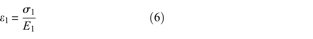
Emerging techniques include embedding miniatured transducers at the adherend/adhesive interface to perform in situ monitoring of the joint strength. Sulejmani et al. 12 embedded three butterfly-shaped optical fiber Bragg grating sensors within a single-lap joint (SLJ) to monitor the shear stress developed under cyclic tensile load. The result shows fair agreement with the Goland–Reissner model along the sensor’s installation path. Zhuang et al. 13 embedded a lead zirconate titanate (PZT) sensor within an aluminum SLJ to monitor the sensor’s electromechanical response with respect to the bonding condition. However, such methods could possibly introduce stress concentrations within the adhesive near the sensor location, leading to embedded defects at the beginning. Some researchers therefore turned to employ nanoparticles for assembling multifunctional, embedded sensors. Naghashpour and Van Hoa 14 mixed multi-walled carbon nanotubes (MWNTs) into the epoxy matrix of glass fiber-reinforced polymer (GFRP) coupons to evaluate the through-thickness strains via measuring the electrical property change. Wu et al. 15 aligned carbon nanofibers (CNF) within a GFRP panel’s epoxy matrix to improve its delamination toughness. Moreover, the aligned CNFs have significantly improved the electrical conductivity of the GFRP panel, over which the internal crack growth and possibly delamination can be monitored. Similarly, some researches modify the electrical properties of adhesives to perform damage assessment of a joint. Ladani et al. 16 embedded CNFs to a two-part epoxy for joining two CFRP substrates as a double cantilever beam under cyclic fatigue testing. The result shows that the aligned CNFs improved the fracture resistance of the adhesive, and enabled in situ crack growth observation. Lim et al. 17 mixed MWNTs into the epoxy adhesive used for joining a composite-to-metal SLJ. The conductivity path created by MWNTs enabled in situ gage-resistance measurement to evaluate different failure modes of the hybrid joint. Mactabi et al. 18 used the similar technique to monitor the electromechanical behavior of the MWNT-embedded adhesive under fatigue load, and correlated the gage-resistance change to the SLJ’s remaining fatigue life. All the aforementioned studies are based on correlating a single gage-resistance measurement to the corresponding damage situation.
In this study, a new approach is attempted to embed an ultra thin layer of nanomaterial over the entire adherend/adhesive interface to avoid introducing stress concentration. An inkjet-printed carbon nanotube (CNT) thin film is embedded at the interface between the adherend and the adhesive to reconstruct the in-plane strain distribution caused by a static tensile load. CNTs possess outstanding electromechanical properties that can be fabricated as strain sensors. 19 The percolated network of CNTs forms a continuous electrical path connected by CNT overlapping. Once a strain is applied, individual CNTs are reoriented, changing the electrical properties (i.e. the bulk resistivity) of the entire CNT network. This is called the tunneling effect of a CNT nanocomposite that dominates its piezoresistive nature. 20 CNT-reinforced polymers can be assembled into thin sheets via spin-coating, 21 layer-by-layer (LbL) method, 22 or compressed air brushing.23,24 These nanocomposites are effective impact damage sensors when coupled with electrical impedance tomography (EIT).22,23 EIT is an algorithm that reconstructs the spatial conductivity change of a defined body using boundary voltage response.25,26 It can be used to identify localized conductivity change due to an impact damage owing to the material’s piezoresistive nature. However, these approaches either have manufacturing restrictions over the CNT embedded thin film’s size and the geometry, or lacks precision control for uniform thicknesses.
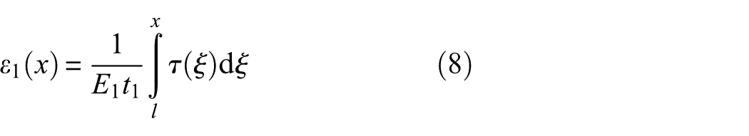
On the contrary, inkjet-printing is a cost-effective method to pattern nano-size particles with high precision.27–29 The electrical properties of the printed layer can be easily tuned by selections of nanomaterials and its concentration in the ink, or by the number of layers to be printed. Previous studies on inkjet-printing silver nanoparticles have shown great potentials over manufacturing flexible electronics. 28 Bekas et al. 30 inkjet-printed conductive silver wires over polyamide thin sheets to connect PZT transducers surface-mounted over a carbon fiber-reinforced polymer (CFRP) coupon. The printed silver traces are reliable, flexible, and lightweight that are ideal for aircraft application. Zhang et al. 31 inkjet-printed silver nanoparticles over polyethylene terephthalate substrates to manufacture lightweight strain gages for aerospace structures; the printed strain sensors achieve higher strain sensitivity (i.e. 3.7) and improved fatigue resistance (i.e. up to 105 strain cycles). Lee et al. 32 also inkjet-printed silver nanoparticles directly over GFRP and CFRP coupons as strain gages, whose gage factor can be tuned by sensor geometry. Similarly, inkjet-printing CNTs yields comparable sheet resistance as low as 78 Ω/sq. 27 Zhao et al. 33 inkjet-printed CNT embedded thin films as spatial strain sensors to map uniform conductivity change, which is correlated to a uniform strain distribution under a tensile load. Gschossmann et al. 34 shows that they could also reconstruct the conductivity change from nonuniform distributed strains, for example, from bending. Therefore, the research interest of this study is to explore its potential as a spatial strain sensor to be embedded within an SLJ.
A CNT-polymeric embedded thin film was inkjet-printed over a glossy photo paper, which is the adherend in this study. MWNTs were mixed with a Pluronic solution to make the ink, and a commercially available printer with a piezoelectric printer head was employed to print the CNT embedded thin film. Another piece of glossy photo paper was adhered over the CNT embedded thin film to create an SLJ specimen, which was tensile loaded. A total of 16 electrodes were wired along the CNT embedded thin film’s boundary to collect voltage data for the EIT analysis. A second specimen was prepared with the same procedure, but a disbonding was introduced by inserting a teflon paper between the CNT layer and the adherend. More details of the test setup can be found in the following sections. EIT reconstruction results will be presented and discussed. An FE model of the testing specimen was created using Abaqus FEA, and the simulated results will be compared with EIT results.
Physical background
Shear strains developed within an SLJ
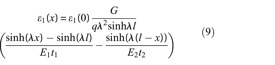
This section presents the one-dimensional stress analysis model of an SLJ (neglecting off-set moments), usually known as the Volkersen model.3,35Figure 1 shows the typical configuration of an SLJ. A uniaxial tensile load, F, is applied to the adherends as shown, developing a shear stress in the adhesive, which is equivalent to that at each adherend/adhesive interface. This shear stress has a nonuniform distribution across the entire area, whereby its mean value,
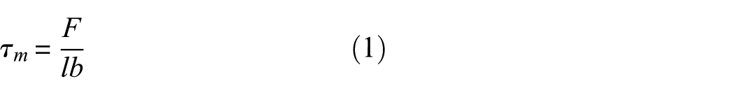
where l is the length of the interface, and b is its width. The shear stress,
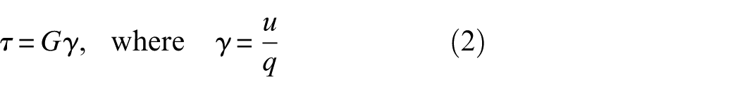
where G is the shear modulus of the adhesive, and
where
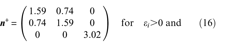
where
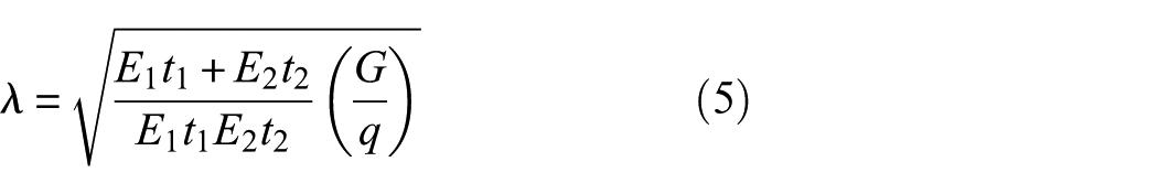
where
where
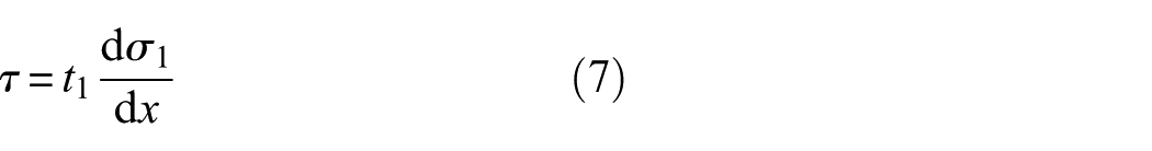
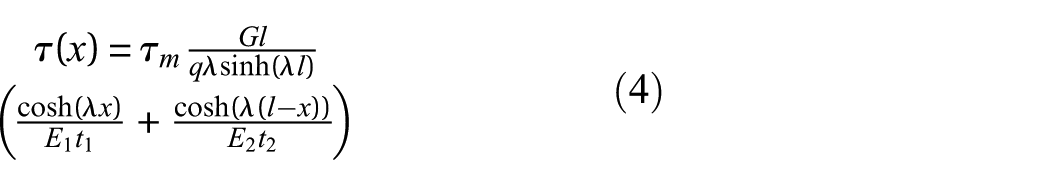
Combining equations (6) and (7),
which fulfills particularly the free boundary condition
where
The bottom diagram in Figure 1 plots the result of equations (9) and (10) with respect to the normalized length of the adherend–adhesive interface. Note that the in-plane strain at the free end (i.e.
The illustration shows the loading configuration of a single-lap joint. A carbon nanotube thin film is embedded between the bottom adherend and the adhesive. The calculated shear stress developed at the thin film–embedded interface is plotted below. The bottom plot shows the in-plane strain distribution developed by the applied force, F.
Moreover, it should be mentioned that bending usually takes place over a tensile loaded SLJ coupon due to misalignment of the acting loads (i.e. due to the off-set moment). The model presented in this section, however, is entirely based on the assumption that such bending effect is negligible. In practice, an SLJ may fail due to bending-induced peeling stresses rather than due to shearing. Hence the modeling result based on the assumption may not be practical to be compared with experimental results. 1 Analytical models such as the Goland–Reissner model and the Hart-Smith model take the off-set effect into account.3,4 More details will be discussed in the “Results and discussions” section.
EIT
For an electrically conductive body,

Therefore, with a known

where
where
where
Experimental details
Inkjet-printing CNT embedded thin films
To prepare the CNT ink, a stabilizing polymeric solution should be prepared first. Pluronic® F-127 was picked due to its extraordinary ability to stabilize nanoparticles for prolonged shelf life. 33 It is an amphiphilic triblock copolymer whose lipophilic midspan attaches to individual tubes and the hydrophilic tails repel from each other in water. A 2 wt% Pluronic solution was made by mixing the Pluronic® F-127 (Sigma-Aldrich Inc.) powder with deionized (DI) water. The mixture was stirred under 65°C until there remained no visible solids. After cooling it down back to room temperature, a small amount (i.e. about 2.5 wt%) of N-Methyl-2-pyrrolidone (NMP) was added to improve the cohesion between the polymer and the nanotubes. MWNTs (Sigma-Aldrich Inc.) were added to the solution and subjected to a 3-s on, 120-s off tip sonication for 1 h (50% power, Bandelin Sonopuls HD3200). After an additional hour of 3-s on, 3-s off tip sonication under the same power, the mixture exhibited a uniform and sleek texture. After two rounds of 30 min centrifugation under 3000 r/min, the supernatant was collected, filtered with a 5 µm PTFE filter, and filtered again with a 1.2 µm filter. The final mixture has a uniform texture with no visible precipitates.
As mentioned in the earlier section, a piezoelectric inkjet printer was chosen for this study; this is because Pluronic is sensitive to temperature, where a thermojet printer head may impact the texture of the ink due to the high heat required. An Epson XP-322 Home Edition printer was used to print the CNT embedded thin film over Sigel glossy photo paper. Comparing to engineering materials such as aluminum and composites, photo paper has a lower stiffness that gives significant stress concentrations along the edges, as depicted in the
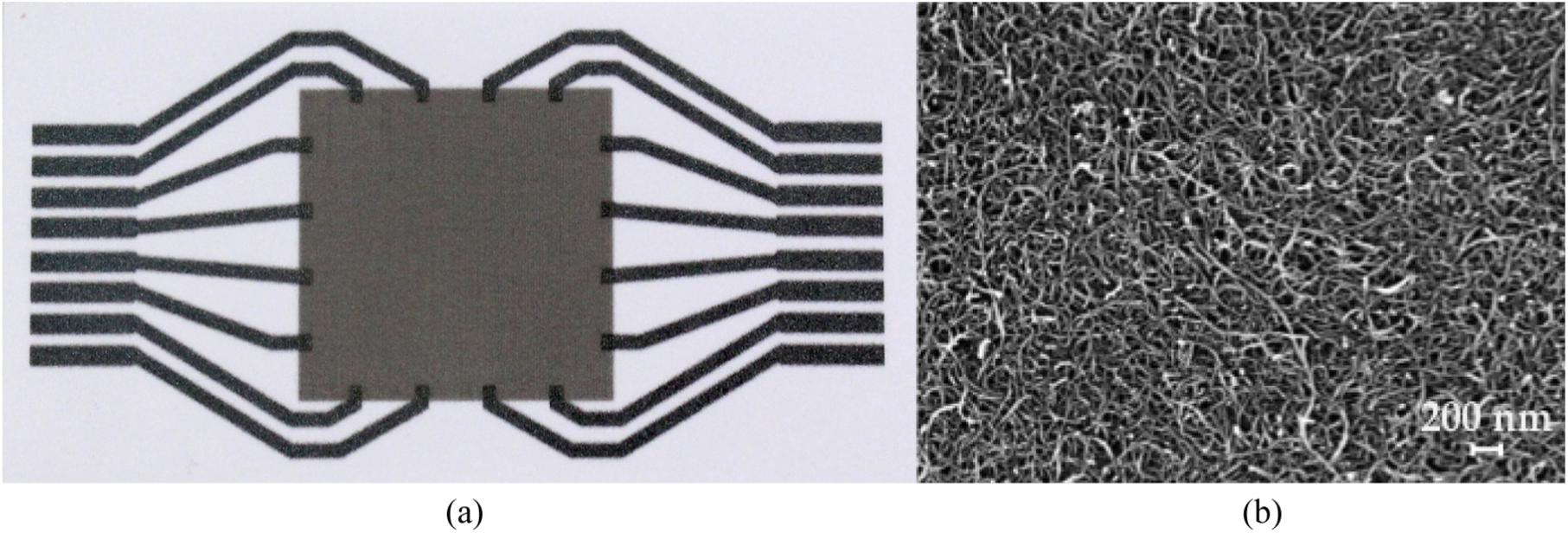
(a) An inkjet-printed CNT embedded thin film with 16 peripheral electrode path contacts to a cumulative plug-in point is shown. (b) The scanning electron microscope image of the CNT embedded thin film shows a uniformly distributed CNT network.
SLJ shear strength test
Figure 3 illustrates the layout of an SLJ tensile test specimen prepared for this study. A 25 × 25 mm2 CNT embedded thin film was printed over a Siegel glossy photo paper with 16 electrode paths as shown. The paper was then cut into a 25 × 100 mm2 coupon with the space of all the electrodes reserved for FFC connections. A thin layer of cyanoacrylate-based, cold-curing adhesive (HBM Z70) was applied over the CNT embedded thin film, with another 25 × 100 mm2 photo paper coupon covered on top. Note that the specimen was prepared so that the two adherends were only adhered over the CNT embedded thin film’s printed area. This is to ensure that the reconstruction map represents the entire adherend/adhesive interface. Figure 4(a) shows a prepared specimen before loading.
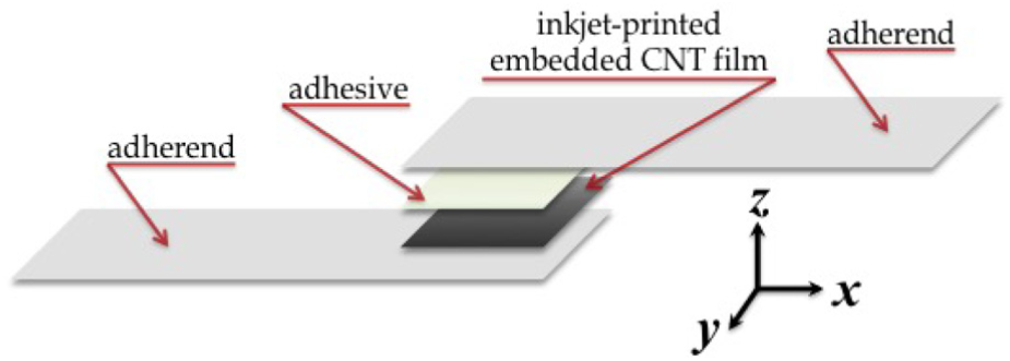
The schematic sketch illustrates the investigated single-lap joint configuration.
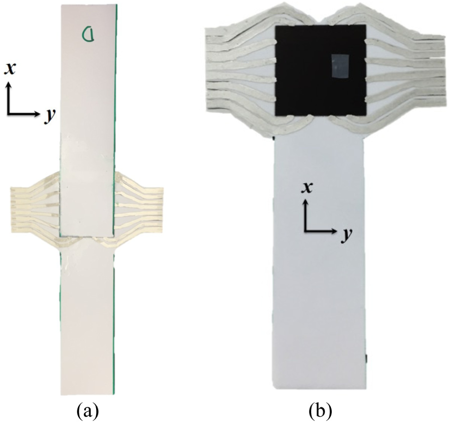
(a) An SLJ specimen is prepared to be loaded. Two 8-pin FFC connectors are used to wire the electrode paths at both sides to the DAQ system and (b) a piece of Teflon paper was embedded between the adhesive and the CNT embedded thin film as shown.
A defected specimen was also prepared. To create a disbonding region at the interface, a Teflon paper was placed over the CNT embedded thin film as seen in Figure 4(b) and embedded. Hence the size of the disbonding area is expected to be in similar size of the Teflon paper. To apply a static load, a constant weight force of 37.14 N was clamped at the end of the specimen, which was pin-fixed over a horizontal rod at the other end. The weight stopped swinging usually after 30 min, and an EIT boundary voltage measurement was subsequently taken.
The voltage data were collected by an HBM QuantumX data acquisition system with a ±10 V voltmeter bridge. The CNT embedded thin film was connected to two 16-to-1 CMOS switches for current injection and voltage measurement. The first switch controls the current injection pattern to create the electrical field over
Results and discussions
EIT reconstructions
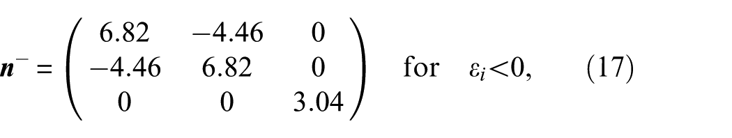
Figure 5(a) and (b) plots the EIT reconstruction results of the healthy specimen and the defected specimen after being loaded for 30 min, respectively; Figure 5(c) and (d) plots additional EIT results of the same specimens shown in Figure 5(a) and (b), respectively, undergone additional loading tests. The dashed rectangle in Figure 5(b) and (d) marks the size and the position of the embedded Teflon paper. All results show a negative contrast change, indicating the load having induced a tensile–strain distribution over the bonding area. Significantly larger contrast change is observed in Figure 5(a) and (c) over the free-end edge (i.e.
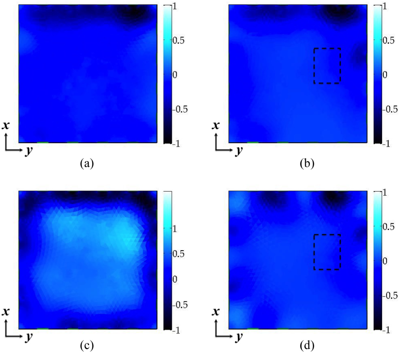
The EIT reconstruction results show that the peeling effect dominates the contrast change of (a) the healthy specimen and (b) the defected specimen. (c) and (d) EIT results of the healthy specimen and the defected specimen, respectively, from additional tests.
On the contrary, the defected specimen shows a similar trend of larger contrast near the top of the sensor, but in a less intensity than that of the healthy specimen. It could be explained by the less-efficient load transfer caused by the existence of the disbonding area, especially the region right above that. By comparing Figure 5(b) and (d) to the baseline result presented in Figure 5(a) and (c), it can be concluded that EIT is able to capture the inefficiency of load transfer due the presence of the disbonding area, of which neither the exact location nor the size can be nevertheless identified at this moment. However, the results demonstrate that the CNT embedded thin film can be applied as a useful monitoring layer to interrogate the sandwiched bonding area, identifying possible occurrence of disbonding. To further correlate EIT results with the strain distribution of the specimen, an FE model was built to simulate the test, and the results are presented in the next section.
FE simulation
To verify the EIT results, an Abaqus three-dimensional (3D)-FE model of the testing setup was constructed for stress analysis. The planar strain distribution over the bottom adherend was calculated. In the following discussion, only the strain distribution over the region covered by the CNT embedded thin film will be presented. To model the specimen, a C3D20R element for 3D stress analysis was chosen with quadratic shape functions, and the tie constraint was used between the adhesive and the adherend. The specimen was modeled to be pin-fixed, and loaded with a surface traction of 37.14 N along the length of the adherend, as seen in Figure 6(a). For the defected specimen, the region of the disbonding area was modeled as absence of the adhesive material. The dimension of the disbonding area is 5 mm × 6.7 mm, which matches the size of the embedded Teflon paper; it locates at the same spot where the Teflon paper was placed within the bond in the experiment. Figure 6(b) illustrates the FE analysis result after the tensile load being applied. For comparison purposes, both FE models of the unloaded and loaded specimen are shown. A through-thickness deflection can be observed, indicating the existence of specimen bending (and thus the peeling stress) due to misalignment, which was discussed in previous section.
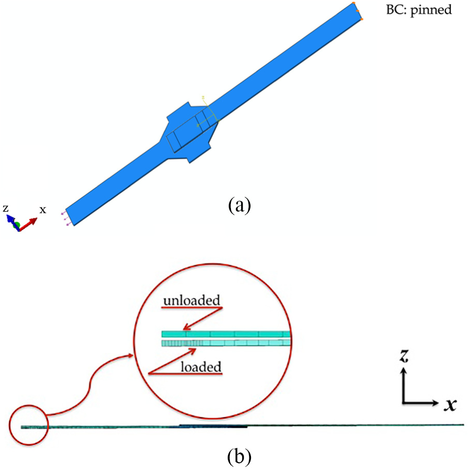
(a) An Abaqus 3D FE model is constructed to simulate the testing scheme of the SLJ. A surface traction of 37.14 N is applied at the end of the thin-film applied adherend, and a pin-fixed boundary condition is applied at the other end. (b) The FEM analysis shows the deflection of the specimen due to misalignment.
However, it should be noted that the EIT reconstructions cannot be correlated directly to a spatial, or specifically, planar strain-state. After being loaded, the conductive body’s electrical behavior becomes anisotropic, and it actually can no longer be modeled as a scalar as it is assumed in equation (15). 39 However, the strain-state is a tensor quantity. Hence, the change in reconstructed conductivity shall either be correlated to an equivalent and invariant scalar quantity of the strain-state, such as its determinant, or the correlation between the actual anisotropic conductivity and the strain-state shall be accurately considered as a tensor. The latter approach has been chosen in recent studies of the authors to characterize the elastoresistivity matrix of the inkjet-printed CNT embedded thin films. 40 It was found that under pristine conditions, the CNT embedded thin film exhibits isotropic electrical behaviors, that is, the resistivity of the CNT embedded thin film is not direction-dependent. However, once it is tensed and therefore stretched in different directions due to Poisson’s effect, the resistivity changes due to its piezoresistive nature and becomes direction-dependent. Moreover, it was also discovered that the CNT embedded thin film holds higher sensitivity to compressive strains than to tensile strains, similar to many other CNT nanocomposites. Therefore, the following elastoresistivity matrices were characterized in Zhao et al.: 40
where
where

In this study,
According to Hamilton et al., 41 a unique solution for solving an EIT problem over an anisotropic body is lacking; therefore, a solution with isotropic assumption would effectively calculate the determinant value of the anisotropic tensor, and that is the result calculated from equation (20).
Figure 7(a) and (b) plots the square-roots of determinant of the anisotropic resistivity tensors calculated by equations (16) to (20) for both specimens based on their FE models. The dashed rectangle in Figure 7(b) marks the size and the position of the embedded Teflon paper. Similar to EIT reconstructions, the highest contrast change takes place along the free end of the adherend at
The plots show the determinant values of the resistivity tensor derived from the strain tensor which was calculated from the FE models of (a) the healthy specimen and (b) the defected specimen. (c) and (d) The 3D versions of (a) and (b), respectively.
Much milder contrasts are also observed along the other three edges with a narrower band, forming a contour-shaped contrast change as observed in Figure 7(a) and (b). This is not perfectly captured by the EIT results, possibly due to its low sensing resolution. By comparing Figure 5(a) to 7(a) and (c), it can be seen that EIT did not show much of the contours suggested by the FE model. This can be explained by the oversmoothing effect from the linearization of the MAP method, where the edge of a sharp contrast jump can be linearized into a gradual slope, resulting in a more enlarged area of conductivity change than it actually is.
42
The contrast change along the edge at
Nevertheless, the contrast changes along
Conclusion
In this study, a CNT embedded thin film was inkjet-printed over a glossy photo paper to monitor the spatial strain distribution over the bonding area of an SLJ. Comparing to other devices that can be embedded within an SLJ, the CNT embedded thin film is an intrusion-free, lightweight layer that can perform in situ monitoring of the in-plane strain distribution caused by static loads. While paired with the algorithm of EIT, the CNT embedded thin film can be instrumented to reconstruct the spatial strain distribution over the joint, providing a deformation map to identify adhesive failures. It should be pointed out that the electrical properties of a loaded CNT embedded thin film are anisotropic. The EIT reconstruction therefore maps a scalar resultant of the conductivity-state tensor, which can be correlated linearly from its strain-state tensor via a rank-four elastoresistivity matrix. To verify the hypothesis, an FE model was built to simulate the testing setup. The models suggest that a cohesive disbonding near the center of the bonding area may not significantly influence the bonding strength. The strain-state data over the CNT embedded thin film’s covering area was evaluated and correlated to the conductivity-state, for which the determinant value was then calculated and mapped. The map is found to be in fair agreement with the EIT reconstruction results, and discrepancies may come from the low sensing resolution of the CNT embedded thin film and the oversmoothing effect of the EIT solver.
The study has demonstrated the spatial sensing capability of an inkjet-printed CNT embedded thin film, and its potential as a nonintrusive, in situ strain monitor for a single-lap adhesive joint. By comparing the EIT reconstructions and the FE analysis results of a defect-embedded specimen to a baseline measurement, it is validated that the CNT embedded thin film can detect the existence of possible disbonding or defects at the joint interface; however, it still remains challenging to use the technique for damage localization. Future research will seek possibilities to apply the sensor for cohesive damage identification, and its application to practical joint structures. To be more specific, experiments on characterizing the CNT embedded thin film’s electrical performance over environmental condition changes and fatigue loads are necessary to determine its optimum application in practice. Moreover, improvement over the resolution of the EIT solver will be also considered. Different regularization methods will be explored to solve the EIT calculation, such as the compressive sensing method.
Footnotes
Declaration of conflicting interests
The author(s) declare(s) that there is no conflict of interest.
Funding
The financial support by the Christian Doppler Research Association, the Austrian Federal Ministry for Digital and Economic Affairs and the National Foundation for Research, Technology and Development is gratefully acknowledged.