
Abstract
In this subject, thermosonic flip-chip technology was introduced to conduct low-temperature bonding of Ag paste and chip interconnection experiments with micro solder joints. The coating and printing method is used to realize the uniform coating of the Ag paste on the micro Cu pillars, and the thickness of the coated Ag paste can be controlled. During flip-chip bonding, different power, pressure, temperature, and bonding time will affect the shear resistance of the solder joint after bonding. Therefore, this article controls the above factors and only studies the impact of ultrasonic power and pressure on the shear force of the solder joint interface. The experiment found that before reaching the maximum shear force, as the ultrasonic power increases, the shear resistance of the solder joint also gradually increased. After that, as the ultrasonic power increased, the shear resistance of the solder joints gradually decreased. It shows that when using thermosonic flip-chip technology for chip bonding, the ultrasonic power should be maintained in an appropriate range to make the bonded flip-chip solder joints obtain a maximum shear strength. The bonding pressure is proportional to the shear strength of the solder joint.
Preface
In the process of flip-chip interconnection, the main interconnection material is alloy solder. With the deepening of research on new silver paste, silver paste has been applied in many fields. There are relatively few research reports on using silver paste instead of alloy solder for flip-chip bonding. In this project, commercial silver paste is used instead of traditional solder to be coated on the solder joints, and the chip interconnection is performed by thermosonic flip-chip bonding. Experiment and study the process of solder joint sintering based on experimental data. The introduction of ultrasound into the bonding process has the advantages of low cost, non-toxic, and harmless, and ultrasonic vibration helps to remove the oxide layer on the surface and expose the pure metal, which is beneficial to the surface diffusion between metals. 1 Other bonding methods generally have the disadvantage of rapid temperature rise, which will rise to a very high temperature in a short period of time, resulting in the thermal decomposition rate of the dispersant being too fast and the formation of large holes in the silver paste interconnection layer. This will cause thermal shock to the device and cause damage to the chip. It has been reported in the literature that when ultrasonic is introduced into aluminum wire bonding, the interface temperature rises only 70–80°C, 2 which is a gentle process.
Flip chip production
The chip processing is mainly based on the process provided by Wuxi Huajin Semiconductor Packaging Pilot Technology R&D Center Co. Ltd., and the post-processing of the chip is completed in this laboratory. It is based on Si, the bumps are Cu pillars, 230 micro Cu pillars are distributed on the surface, the bump diameter is 40 μm, the copper pillar height of the upper chip is 30 μm, and the copper pillar height of the lower chip is 10 μm. The distance is 200 μm. This chip is characterized by high bump density and small distance between bumps. The customized chip is shown in Figure 1. Customized chip.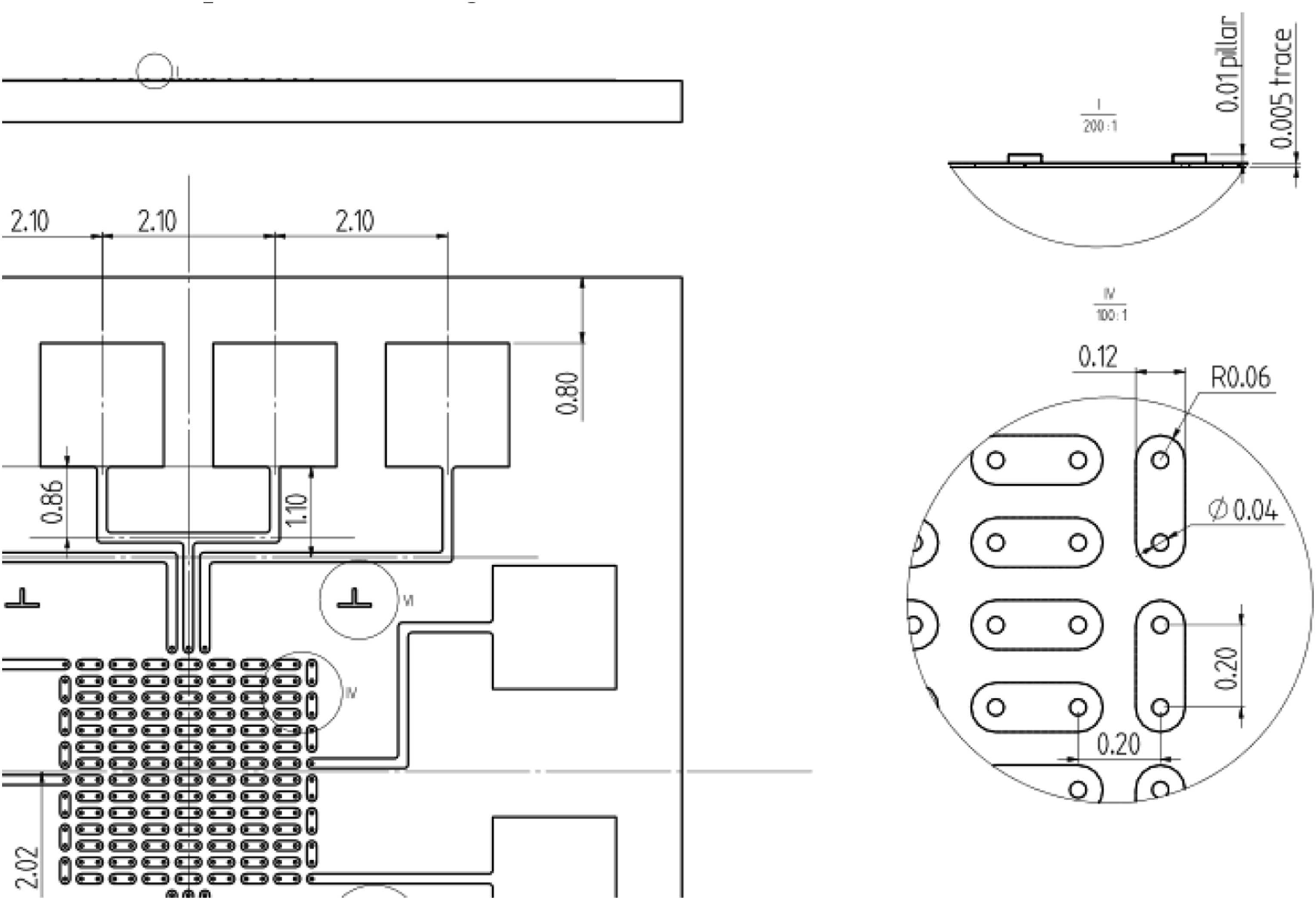
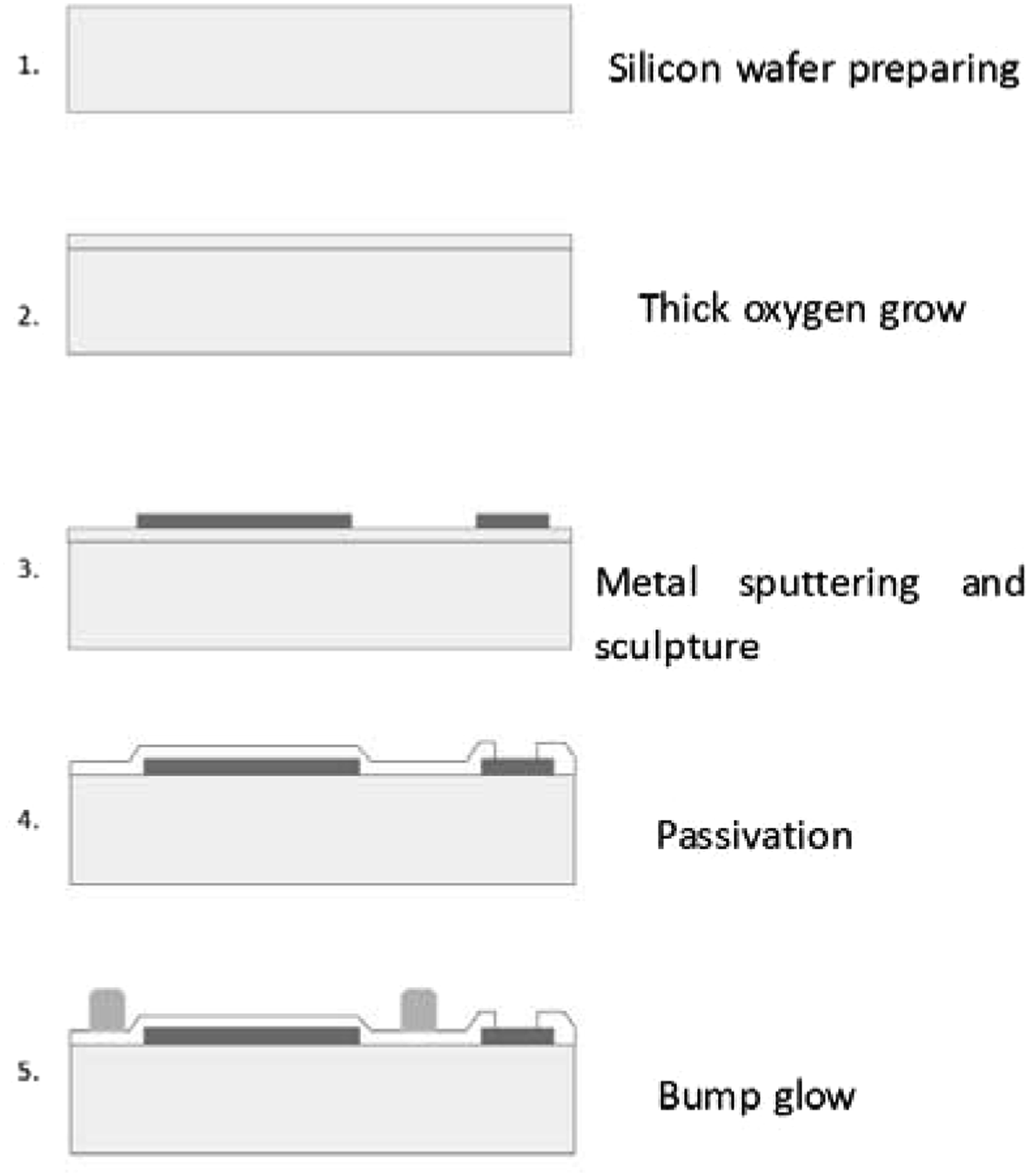
The process flow of the chip is shown in Figure 2.
3
First, the silicon wafer is oxidized, the process temperature is 1200°C, the oxidation time is 3 h, and the thickness of the oxide layer is about 1 μm; followed by sputtering metal and etching out electrode plates and connecting wires; then passivate the chip and use chemical vapor deposition to deposit SiN with a thickness of 1–2 μm to form a passivation layer; and finally photoetch out the pads and pads. After the chip is processed here, all the previous processes are completed, and then the processed silicon wafer must be taken to the electronic packaging factory to complete the preparation of bumps. The previous process parameters and steps are as follows: (1) Silicon wafer preparation. Conventional silicon wafers have a thickness of 500 μm. (2) Thick oxygen growth (thickness l μm). Dry oxygen oxidation is a commonly used growth method. When oxygen is in contact with silicon wafers at high temperature, oxygen molecules react with silicon atoms on the surface to form a silicon dioxide starting layer. The characteristics of gate oxide prepared by this oxidation method are the structure is dense, but the temperature is high and the oxidation rate is slow. (3) Cr and Au metal sputtering and etching (thickness 500 Å+2000 Å). The internal channels of semiconductors consist of tens of thousands of meters of metal wires, and sputtering targets are a key consumable material for making these wirings. These wires must be splashed onto a high-purity wafer and etched to form individual wires. The sputtering target is the core of semiconductor wafer manufacturing, and the chip has high requirements on the purity of the sputtering target. (4) Passivation. The chemical vapor deposition method is used to deposit SiN with a thickness of 1–2 μm on the chip to form a passivation layer, and the metal is passivated to form a protective film. (5) Photolithography etching silicon nitride. The pads and the pads that will be connected to the bumps are photoetched in preparation for the bumps. Substrate process flow chart.
3
In order to improve the reliability of the bump, an under bump metal (UBM) is also made between the bump and the pad. The bottom metal generally uses Ti as the adhesion layer and the bimetal structure of the barrier layer and the soldering layer. The bonding effect of Au and Pb–Sn alloy is not good, and solder is generally not used on gold bumps. Using Cu as the base, there is no remelting phenomenon, and its aspect ratio is high; in addition, it can play a stable supporting role and improve the reliability of the solder joint, as shown in Figure 3. The main processing of Cu is also in line with the trend of mainstream high-speed integrated circuits. Schematic diagram of columnar bump structure.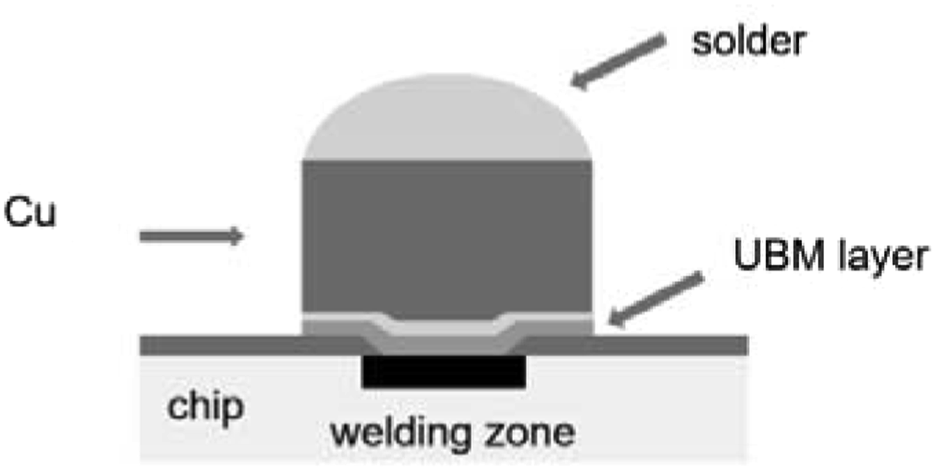
If the flip-chip solder joints are electroplated, it is like preparing a copper connection line in an IC, using a pattern transfer method to make the necessary patterns on the surface of the Si wafer.
The process flow of flip-chip solder joints is shown in Figure 4, including pre-cleaning-UBM layer metal Ti, Cu sputtering- coating- exposure- development- photolithography inspection-plasma removal-copper plating -Remove glue-etching. Process flow of columnar bumps.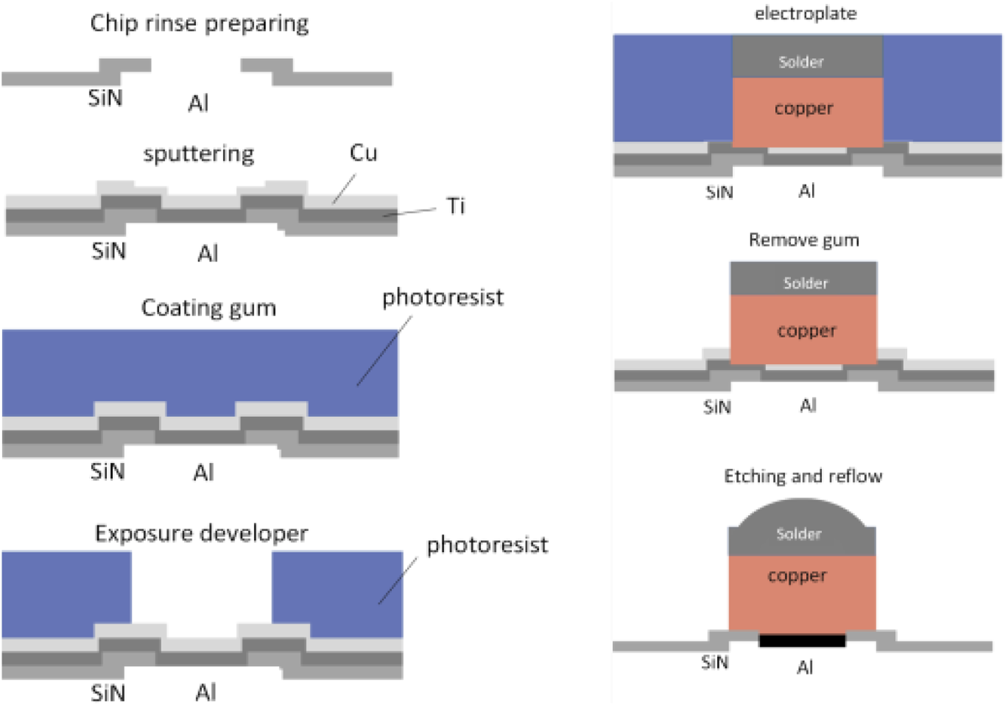
After electroplating the copper pillars, silver paste is used instead of alloy solder to coat the chip bumps. Professor Li Junhui of Central South University
4
has conducted in-depth research on flip-chip solder coating. The process of silver paste coating is spread silver paste in a groove and then use a glass plate to smooth the silver paste. Place the bumps of the upper chip downward and horizontally on the silver paste to ensure that each bump can fully contact the silver paste. After the silver paste is applied, the scanning electron micrograph of the chip bumps is shown in Figure 5.
5
Scanning electron microscope image of silver paste coated on bumps.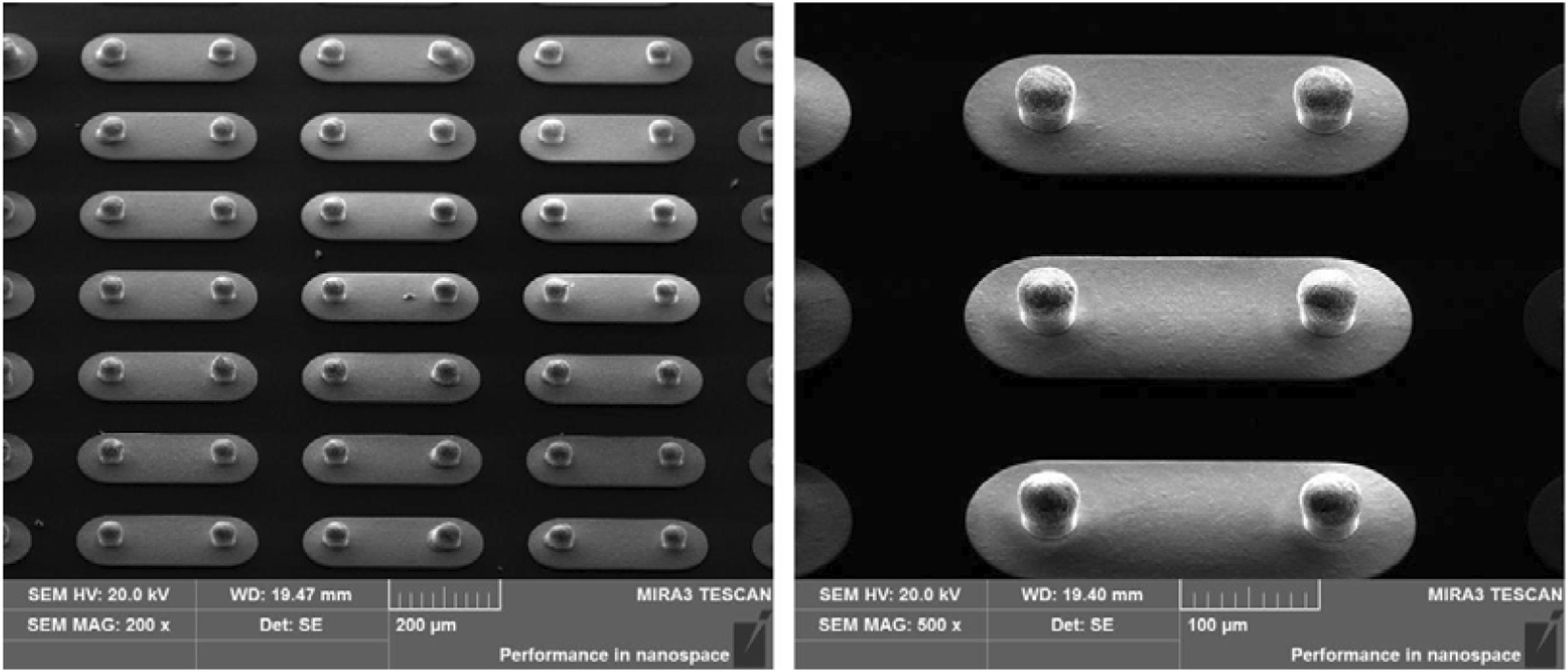
Introduction to thermosonic bonding technology
This technology draws on thermosonic wire bonding technology. Under the action of ultrasound, the substrate is heated, and then the chip that has been implanted with metal bumps is turned over and bonded to the substrate pad by bonding force. This bonding technology has the following advantages: (1) It belongs to the method of array interconnection, which does not use lead-containing solder and does not require glue filling; (2) Ultrasound is the most bonding power, which directly simplifies the process, so that the chip and substrate are protected from damage in a short time; (3) Shorten the process cycle; (4) Strong compatibility, compatible with thermosonic wire bonders, flip-chip bonders, and other equipment; (5) The introduction of ultrasound accelerates the bonding process and reduces the heating temperature of the substrate.
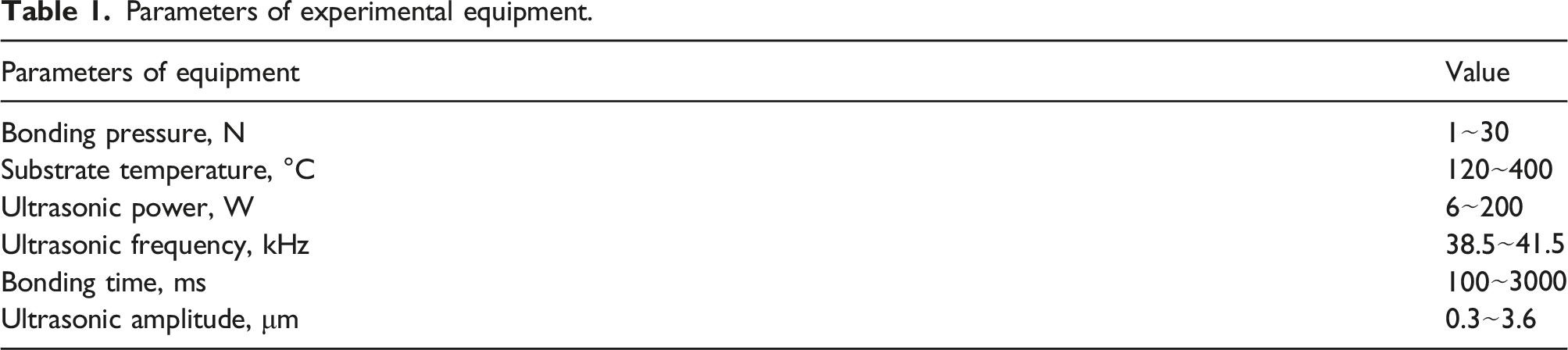
Because of these advantages, the thermosonic flip-chip bonding technology has become a widely used chip bonding technology. The flip-chip bonding experiment equipment used in this experiment is shown in Figure 6. It is a flip-chip bonder (Flip Chip Bonder) produced by Japan’s Athlete Company. Its model is CB-600 with an accuracy of 1 μm. Other parameters of the equipment are shown in Table 1. Actual flip-chip test bench. Parameters of experimental equipment.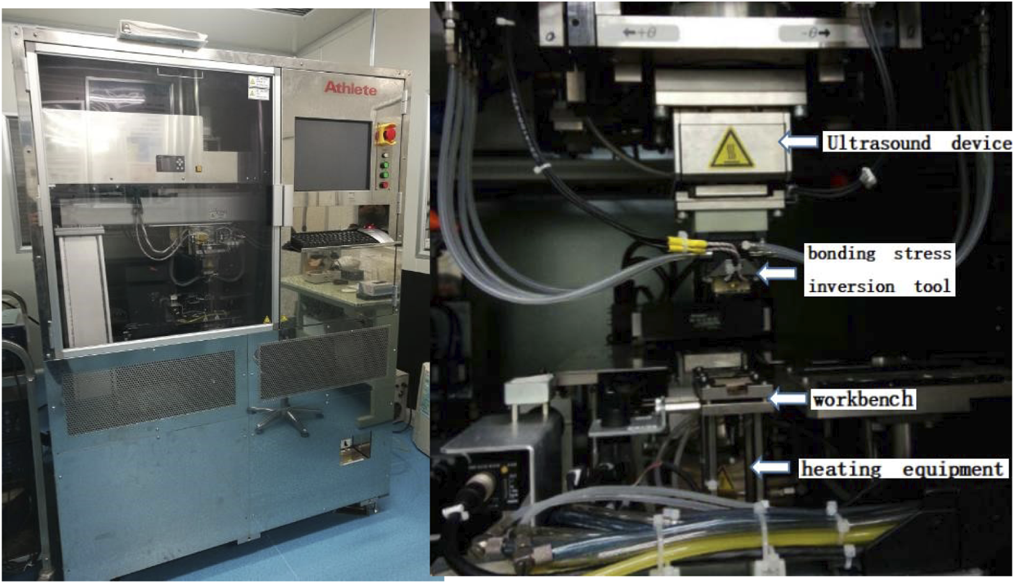
Thermosonic flip-chip bonding experiment
Chip bonding process
During the preheating process, the temperature should be raised to about 200°C. When the temperature reaches the preheating setting value, the upper chip is lowered and contacted with the lower chip, and then a certain bonding pressure is applied. When the bonding pressure reaches the preset value, ultrasonic vibration is introduced into the bonding process. The ultrasonic application time is about 1–2 s, as shown in Figure 7. At the same time, the heating process continued and finally heated to 280°C. Then keep it at this temperature and bonding pressure for 3 min, then stop heating and pressurizing, and let the interconnection chip cool to room temperature naturally. In the bonding process, changes in parameters such as temperature, pressure, and ultrasonic power will affect the bonding quality. The bonding process is completed by exposure to air. Applying ultrasonic bonding pressure.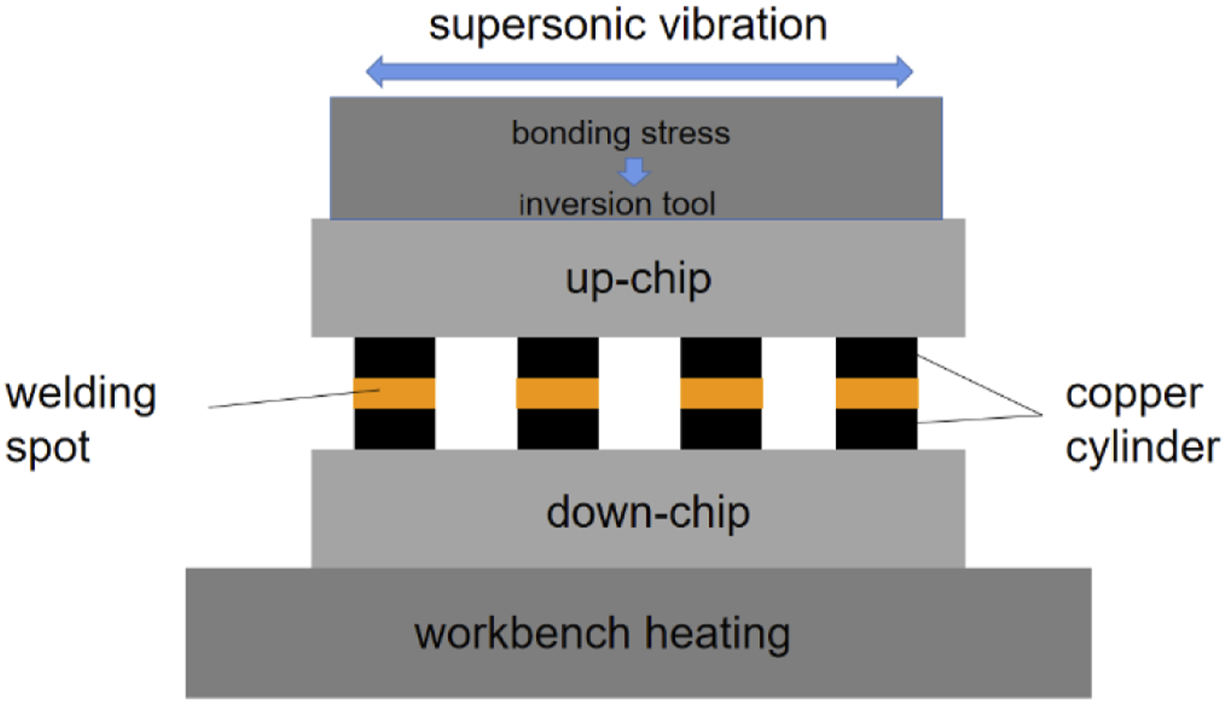
Experimental results
Generally speaking, the effect of flip chip bump welding is often determined by measuring the interconnect strength of flip-chip bumps. Bump interconnection strength testing is often divided into two methods: one method is to measure the shear force and the other method is to measure the tensile force. This experiment uses the first method to test the shear force of flip chip bumps. The effect of thermosonic technology in flip-chip bonding can be estimated based on the measurement results. The focus is on the fracture shear test of the interconnected chips. The measurement of shear force is mainly to determine the resistance to shear of flip-chip bumps. The test is carried out by the tensile shear test machine Dage4000. When testing the shear strength in this subject, the test rate is 500 μm/s, the maximum test load is 76,430 g, and the shear height and test displacement should be set at the beginning of the test.
According to the relevant literature, the changes of ultrasonic power and pressure have a great influence on the bonding strength,6–10 so the two key factors of ultrasonic power and bonding pressure are selected as the experimental control objects and through the previous research experience and the factory reference value to determine the final parameter.
(1) Experimental results of ultrasonic power parameters
Average shear strength of bumps under different ultrasonic power.
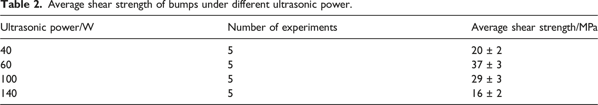
As shown in Table 2, the shear strength of the chip bumps is directly proportional to the ultrasonic power at first, but when it reaches a peak, it begins to gradually become inversely proportional. This result shows that among the ultrasonic powers provided, there is a rising interval in which the interconnected flip-chip bumps have the maximum shear strength of 37 ± 3 MPa.
(2) Experimental results of bonding pressure parameters
Relationship between bonding pressure and shear strength of interconnected bumps.
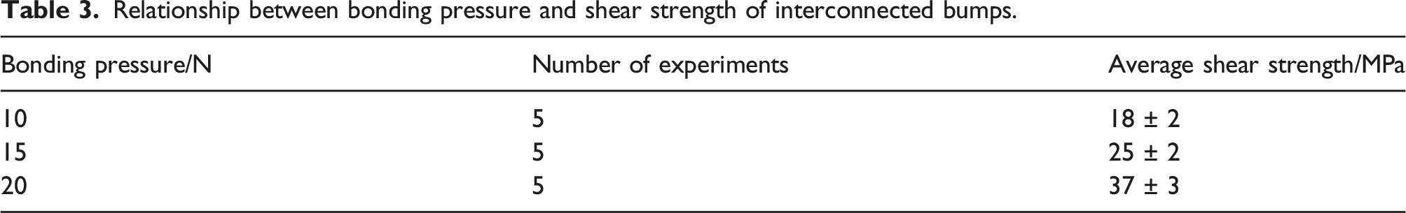
It can be seen from the following table, the shear force of flip-chip solder joints increases with the increase of bonding pressure, and the two are directly proportional.
Experimental mechanism analysis
The flip-chip bonding process is the Ag paste sintering experiment. The sintering process is generally divided into three stages. The first stage has a lower temperature, which is mainly due to the volatilization of the solvent. The second stage is a medium-temperature stage, when the Ag powder contacts to form a sintering neck. The third stage is a high temperature stage, at which time diffusion occurs between the powders to continuously increase the density of the sintered layer. Due to the introduction of ultrasonic technology in the bonding process, the sintering principle of Ag paste is different from the general hot pressure welding method. The surfactant in the Ag paste will prevent the agglomeration of the powder on the one hand and prevent the sintering between Ag particles on the other hand. For smooth sintering, the surface dispersant must be decomposed. The effect of preheating can volatilize the organic solvent in the Ag paste, and at the same time, it can make the flux work to prevent Cu from being oxidized. Ultrasonic technology is generally added after the organic matter in the first stage has evaporated and before the sintered neck grows in the third stage. Ultrasonic action is conducive to the reordering of Ag powder, which will make the powders more compact, increase the chance of contact between the powders, and increase the origin of the sintering neck growth. The sintering neck growth process is shown in Figure 8. In addition, the vibration formed by the ultrasonic process generates heat, which is beneficial to the dissolution of the powder. Cavitation occurs when ultrasonic waves propagate in the liquid solder medium. That is, ultrasonic waves generate periodic tensile and compressive stress on certain fixed points in the liquid phase, which promotes the formation, growth, and explosion of vacuum voids in the liquid phase. And shock waves and micro-jets are generated, accompanied by the conversion of surface energy to chemical energy and thermal energy. High temperature and high pressure are generated locally in the weld, causing the metal particles to rapidly peel off and dissolve.
11
Schematic diagram of sintering neck growth process.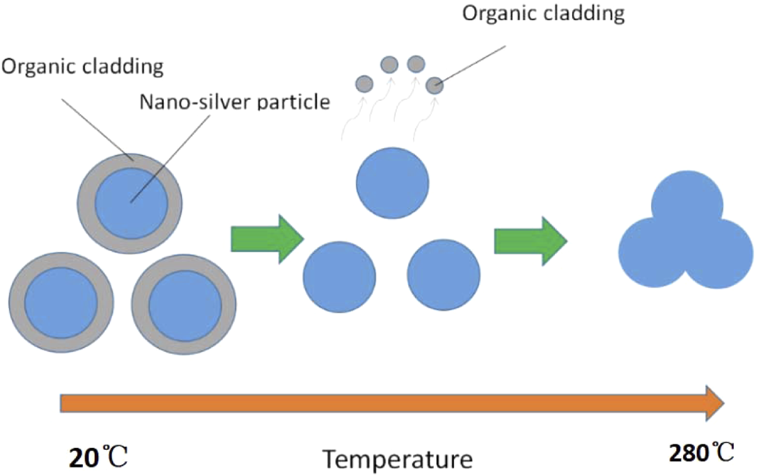
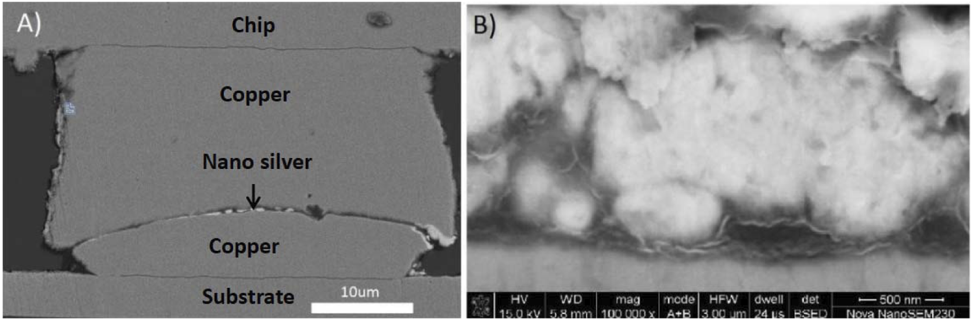
The last stage of bonding is the heat preservation and pressure holding stage in the process, that is, the diffusion process between Cu and Ag particles. The cross section of the sintered layer is shown in Figure 9(a). It can be seen that when a certain bonding pressure is applied, the thickness of the Ag sintered layer formed is in the range of 1–2 μm. From the cross-sectional view, it can be found that diffusion is formed between the Ag powders. The surface of the Ag powder is first melted during the bonding process, and the melted surfaces are connected to each other to create element diffusion channels. After the introduction of ultrasonic technology, the friction between Ag powder and Cu bumps is intensified. The friction effect is beneficial to remove the oxide layer on the copper surface, exposing the pure Cu surface, and promote the diffusion of Ag powder on the Cu surface so that Ag and the increased contact area of Cu is conducive to forming a metallurgical bond, as shown in Figure 9(b). SEM image of sintered layer.
5
Summary
In this subject, thermosonic flip-chip technology was introduced to conduct low-temperature bonding of Ag paste and chip interconnection experiments with micro solder joints. The coating and printing method is used to realize the uniform coating of the Ag paste on the micro Cu pillars, and the thickness of the coated Ag paste can be controlled.
The focus is on the relationship between bonding pressure, ultrasonic power, and sintering strength. When keeping the power constant, the bonding pressure is proportional to the shear strength, that is, the shear strength will increase as the bonding pressure increases. When the pressure is kept constant, as the ultrasonic power increases, the shear strength increases at first, but after the maximum value, it gradually decreases. Under 60 W ultrasonic power and 20N bonding pressure, the average shear strength of the solder joint reaches 37 ± 3 MPa. Without the introduction of ultrasonic technology, the solder joint sintering strength is low. Increasing the ultrasonic power will increase the amplitude, which is not conducive to the bonding of Ag paste.
Ultrasonic technology is conducive to the reordering of the powders, increasing the contact area between the powders and increasing the origin of the sintering neck growth. Ultrasonic vibration intensifies the friction between copper and silver, which is beneficial to remove the oxide layer on the copper surface and promote the diffusion of silver particles on the copper surface. Combine the energy gathering effect, cavitation effect, acoustic flow effect, and interface effect of ultrasonic wave on multiphase melt with the characteristics of hot pressing sintering technology. The interconnection mechanism of ultrasonic-assisted sintering nano-silver paste was revealed by the coupling effect of ultrasonic vibration field, sintering pressure field, and sintering temperature field.
Footnotes
Declaration of conflicting interests
The author(s) declared no potential conflicts of interest with respect to the research, authorship, and/or publication of this article.
Funding
The author(s) received no financial support for the research, authorship, and/or publication of this article.
Data availability statement
The data of this study are available from the corresponding author upon reasonable request.