
Abstract
Electromagnetic pulse welding is a high-velocity impact joining process employed with the intention of forming fast and effective solid-state bonds. Electron microscopy techniques, including SEM and TEM, revealed that bonding was not fully accomplished in the solid state; instead, local melting can occur. These locally melted areas likely occur around the point of first contact during the welding process and are associated with a debonded region that runs alongside or through the centre of melted zones. Microstructural characterisation showed dispersoid-free regions, columnar grains, epitaxial growth, and localised increases in O, Fe, Si, and Mn content in locally melted areas. This region contrasts with the solid-state bonded region, in which the interface exhibited sub-micron grains.
Keywords
Introduction
Electromagnetic pulse welding (EMPW) has garnered interest as it can be utilised for producing joints between similar and dissimilar materials, which are thought to form through solid-state processes.1,2 It is regarded as economical and environmentally friendly, owing to its fast and repeatable operation that requires no filler wire or shielding gas. 1 The lack of heat input in forming a joint is another attractive factor compared to fusion welding techniques where the use of high heat input and deposition of consumables can result in the formation of heat-affected zones and partially melted zones which can cause liquation and other detrimental features. 3 Thus EMPW is thought to be a great advantage for automotive applications which use a range of 6xxx series aluminium alloys especially for electric vehicles which are expected to spearhead the increase in the use of high-strength aluminium alloys.4,5 While EMPW has seen an increase in interest as shown by Kapil et al. 1 , Li et al. 6 argues that there is little published literature on the EMPW of similar metals, they go further by stating how there is still some debate on the occurrence and role of local melting along the joint-interface and how there is no consensus about the necessity of local melting to achieve a strong weld. For example, Li et al. 7 showed through a thermomechanical model that the interface could experience rapid melting and solidification. Alternatively, Aizawa and Okagawa 8 argue EMPW of dissimilar materials often did not cause a high enough temperature increase to result in melting.
Studies7,9,10 which have reported melting state that when it does occur, detrimental intermetallics and amorphous layers can form. Faes et al. 11 found that in dissimilar copper to brass joints, the formation of intermetallics can cause cracks. They also noted how melting had a higher tendency to occur in the areas just beyond the bonded zone. Research on explosive welding of 304SS/Mg has shown evidence of columnar grains indicative of melting, adjacent to fine grains along the joint interface. 12 A study looking at joining similar metals found vortex-induced localised melting in Al/Al welds, causing cracks and voids. 2 Others have found the dissolution of secondary phases at the joint interface10,13 and the formation of porous structures. 14 However, some researchers such as Ali et al. 9 state that local melting is inevitable and is even a prerequisite for bond formation. Stern and Aizenshtein 15 found that for both similar and dissimilar materials, bonding is based on the formation of a thin layer of molten metal. In any case, the most relevant questions are: does local melting occur in similar Al/Al joint, if melting does occur is it a favourable or detrimental feature, and what are the characteristics of the locally melted areas.
Despite the above studies, a direct microstructural comparison between the bonded and locally melted areas in similar high-strength Al/Al joints has not been reported. The present study, therefore, aims to highlight the occurrence and characteristics of locally melted areas along the EMPW interface in similar Al/Al joints, specifically in a commercial alloy and a higher-strength alloy. We take a novel approach by combining characterisation techniques, including backscatter electron (BSE) imaging, electron backscatter diffraction (EBSD), transmission Kikuchi diffraction (TKD), and scanning transmission electron microscopy energy-dispersive X-ray spectroscopy (STEM-EDS), to provide evidence of the microstructural features and key elemental distribution of these locally melted areas and compare them to bonded areas. This allowed us to elucidate how local melting can occur and its association with defects. These findings will provide key insights for those using electromagnetic pulse welding.
Materials and methods
A commercial AA6008 alloy in the T7 temper and an extruded high-strength 6xxx series alloy in the T6 temper were individually joined to identical alloys of their own kind through the EMPW process, yielding an AA6008/AA6008 joint and a high-strength 6xxx/high-strength 6xxx joint. The flyer and target sheets were in the form of 2.5 mm thick extrusion coupons. Joints were created using a pulsed power generator, PS96-16 Blue Wave, with a maximum capacitor charging energy of 96 kJ and a voltage of 16 kV from PSTproducts GmbH. Figure 1(a) shows a cross-sectional view of the setup. A discharge energy of 40 kJ and an air gap of 2.5 mm were used, with the coil producing a primary current pulse approximating a damped sine wave with a peak amplitude of 538 kA and a frequency of 12.4 kHz. The process results in a welded area which is a hollow oval shape (Figure 1(b)). The welded area shape results in two bonded zones on either side of an unbonded zone in the centre; a diagram of the different zones is shown in Figure 1(c). All samples were hot mounted in conductive Bakelite and ground successively using 220, 330, 800, 1000, 1200, and 4000 grit SiC paper. Polishing was done using a ‘Tegramin-30’ with a 3 μm polishing pad for 5 min and then using a 1 μm polishing pad for another 5 min. The final polish was achieved with ‘Mastermet 2’ non-crystallising colloidal silica on a ‘VibroMet 2’ at 80% power for 3 h. BSE imaging was performed using a JEOL 7800F at 10 keV with a probe current of ∼1 nA. EBSD analysis was performed using an ‘HKL Nordlys Oxford Instruments’ detector at 20 keV with a probe current of ∼16 nA and a step size of 0.2 µm. STEM-EDS analysis was performed using an FEI Tecnai F20 at 200 keV. EDS maps are presented as ‘Quant maps’ using Oxford Instruments AZtec software, which show the spatial distribution of elemental concentrations (in wt%). A ThermoFisher Helios G4 CXE dual-beam P-FIB equipped with a Xeon ion source was used to create site-specific lamella, and an ‘Oxford Instruments Symmetry S1’ was used to perform TKD. TKD was done using an accelerating voltage of 30 keV and a probe current of 6.4 nA with a 50 nm step size. Average grain size was determined using the EBSD and TKD data using the maximum fitted ellipse method.
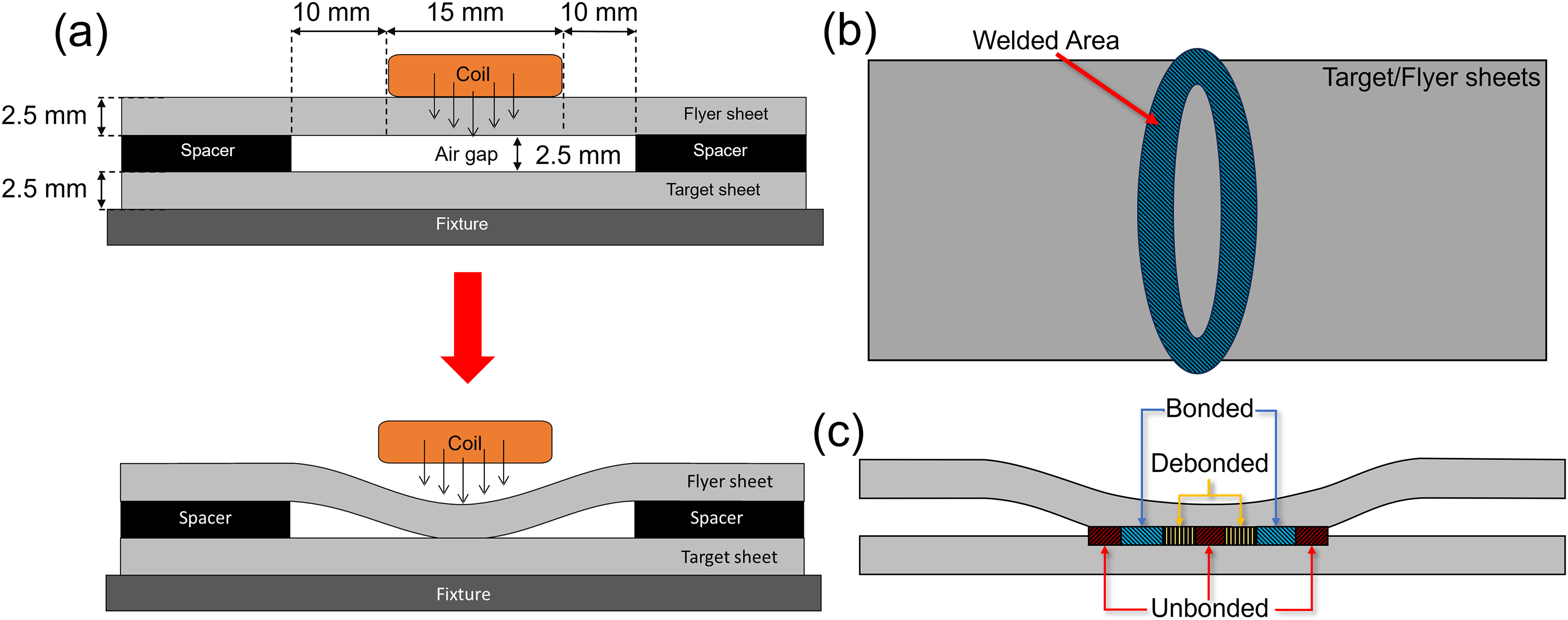
(a) Schematic of EMPW setup, (b) schematic showing a top-down view of the coupons displaying the welded area, (c) cross-section of a typical EMPW coupon showing the location of the three regions across the join-interface: unbonded, debonded, and bonded.
Results and discussion
Figure 2(a) shows a schematic of the features seen along the joint interface. Figure 2(b) and (c) shows BSE image montages of the AA6008-T7 and the high-strength 6xxx alloy-T6 EMPW coupons, respectively, with accompanying high-magnification images of the different regions along the joint interface. The BSE montage of the welds reveals how the lack of heat input, filler materials, and mechanical stirring preserves the structure of the base alloy, especially when compared to traditional fusion welding processes 16 (although it should be noted that this does not show the large amounts of strain that is imparted into the material). The typical dispersoid phase found within these aluminium alloys is α-Al(Fe, Mn)Si type. 17 The dispersoids appear as bright particles in BSE imaging due to the high Fe content. AA6008-T7 is in a recrystallised form, and the high-strength 6xxx alloy-T6 is in an unrecrystallised (fibrous) form. Both alloys have peripheral coarse grains (PCG), which are large, recrystallised grains on the surfaces of the extrusions. These are effectively the surfaces that are bonded during the EMPW process. However, as AA6008-T7 is a recrystallised alloy, the PCG may not appear as visible as it does in the fibrous alloy. Both alloys have an unbonded (UB) region in their centre where the flyer and target sheets did not contact or did not experience sufficient shear strain, collision angle, or the springback phenomenon occurred. 18
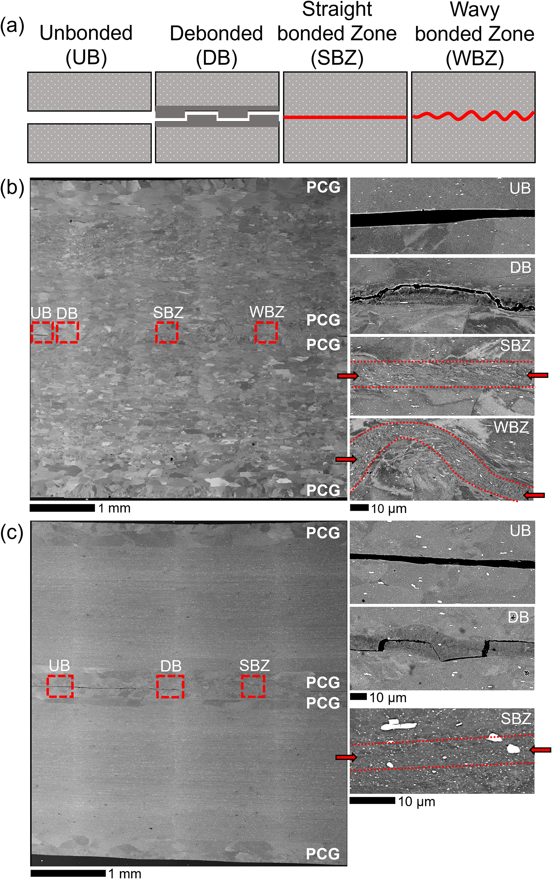
(a) Schematic displaying exaggerated diagrams of various features along the joint interface. BSE montage images alongside higher magnification BSE images of different regions along the joint interface in (a) AA6008-T7 and (b) high-strength 6xxx alloy-T6.
Within the bonded regions, the alloys differ from each other. In the bonded region of AA6008-T7 it shows both a wavy bonded zone (WBZ) and a straight bonded zone (SBZ) (Figure 2(b)), whereas in the high-strength 6xxx alloy-T6, only an SBZ was observed (Figure 2(c)). The occurrence of the WBZ has been attributed to a shock wave which propagates through the material, creating a periodic perturbation at the joint interface. 19 One study found that the occurrence and morphology of WBZs can be affected by impact velocity and impact angle, as these parameters affect the wave parameters (wavelength and amplitude).20,21 Another study suggests that the material properties of alloys can cause differences in impact velocity and impact angle, 22 possibly indicating why the high-strength 6xxx alloy lacks a WBZ.
A debonded zone (DZ) between the UB and the SBZ can be seen in both alloys. This DZ is characterised by debonding occurring along the edge or through the centre of what appears as a dark grey band in BSE imaging. This is more likely to be debonding than a UB zone, as the debonding takes a less direct path, passing along the edge or through the centre of the grey band (Figure 2(b) and (c)). Figure 3 displays higher magnification images of this region, revealing the darker grey band to be a dispersoid-free region (DFR). To resolutionise dispersoids requires a temperature close to the solidus for an extended period of time and given that the process is completed in a fraction of a second, it is likely accomplished by local melting.
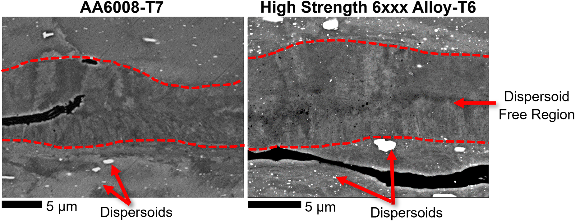
BSE images from within the debonded zone (DZ). Red lines denote the boundaries of the DFR, with red arrows highlighting dispersoids that appear white in BSE imaging.
Figure 4 provides BSE images and the corresponding EBSD inverse pole figure (IPF) maps of the DFR in both alloys, it should be noted that the DFR could occur without debonding but debonding was never observed without a DFR. It can be shown that the DFR is split into two parts, one part shares a similar orientation as its neighbouring PCG. It is likely a part of the PCG that may have partially melted or reached temperatures close to the solidus, resulting in it being dispersoid-free. Figure 4(d) provides further indication of partial melting as debonding appears to have propagated into the PCG, possibly due to partial melting. The other part is made up of columnar grains with individual orientations. Figure 4(c) shows columnar growth with a similar orientation to the parent PCG, suggesting epitaxial growth consistent with melting and resolidification on the parent metal. The size of the two regions is as follows: in AA6008-T7, the partially melted PCG part has an average thickness of 5.3 ± 0.3 µm, and the columnar grains have an average length of 3.2 ± 0.1 µm. In the high-strength 6xxx alloy-T6, these values are 5.0 ± 0.3 µm and 4.1 ± 0.3 µm, respectively.
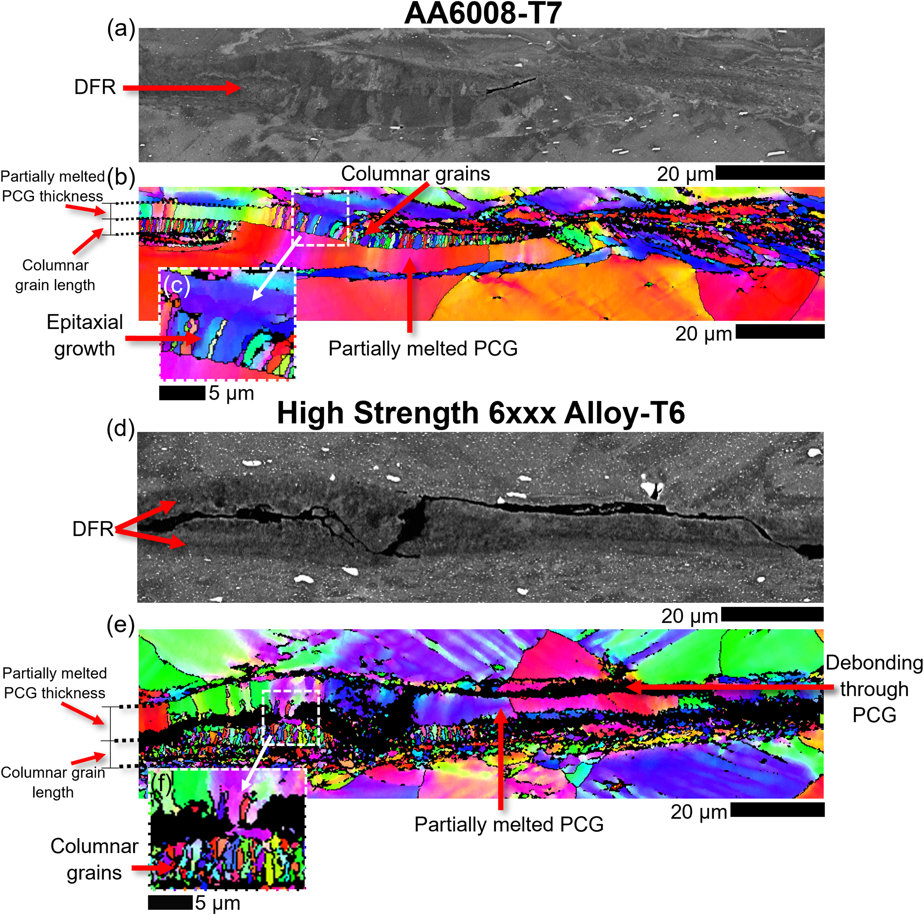
BSE images with corresponding IPF maps of the same area showing the DFR in (a) and (b) AA6008-T7 and (d) and (e) high-strength 6xxx alloy-T6. (c) and (f) present an enlarged section of each IPF map.
Figure 5 provides the IPF and band contrast (BC) maps processed from the TKD data with corresponding TEM-EDS maps taken from a SBZ and DFR. In AA6008-T7, the SBZ is made up of a mix of equiaxed and columnar grains, with an average grain size of 0.6 ± 0.03 µm. In the high-strength 6xxx alloy-T6, the SBZ is made up of fine equiaxed grains, with an average grain size of 0.4 ± 0.01 µm. Studies have shown that the presence of these fine equiaxed grains is due to dynamic recrystallisation, which is a consequence of the accumulation of dislocations and the formation of subgrains.6,23,24 The high amounts of plastic strain at the joint interface result in the sub-grains transforming into dynamically recrystallised (DRX) grains.
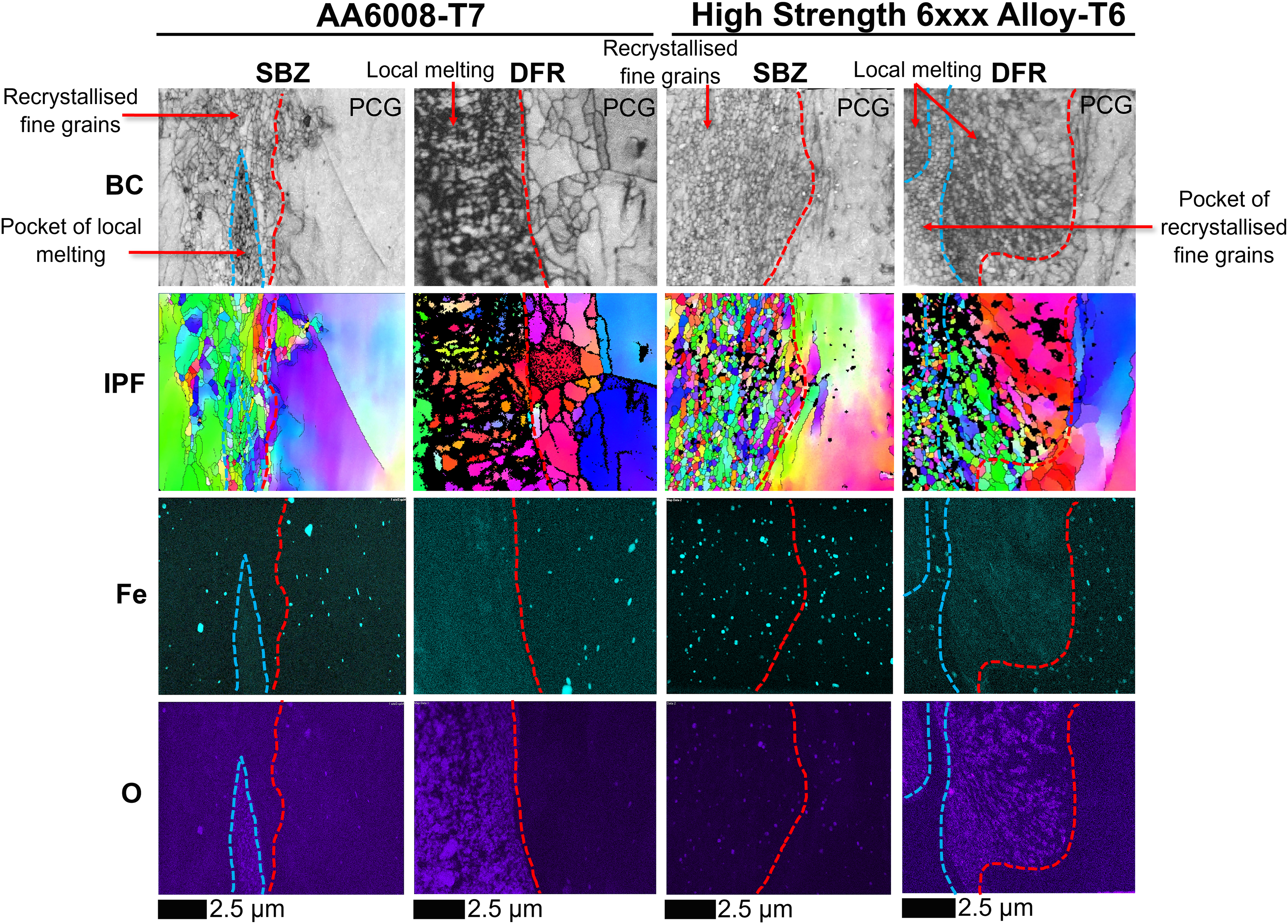
BC and IPF maps obtained using TKD, along with TEM-EDS quant maps illustrating the spatial distribution (in wt%) of Fe and O for the SBZ and DFR in AA6008-T7 and the high-strength 6xxx alloy-T6.
The dispersoids in the SBZ, as shown by Fe EDS maps (Mn and Si maps have been excluded in Figure 5 as they overlap), are continuous; they are present across the joint interface and in the neighbouring PCG. In contrast, the DFRs are made up of columnar grains, and while dispersoids are present in the PCG, they are absent in the area containing columnar grains. Ben-Artzy 13 and Stern 10 found similar results in similar Al/Al joints, observing the dissolution of β-Al5FeSi and Al3Fe , respectively. Stern also noted that Fe was evenly distributed across the melted interface, showing that local melting occurred, and then rapid solidification prevented re-precipitation. This agrees with the present study, where EDS maps also indicate that the melted regions have an increase in Fe content (and by extension Mn and Si), that is, the dispersoid-forming elements. This indicates that when local melting occurs, the dispersoids are rapidly dissolved/melted, and the dispersoid-forming elements remain in solution upon re-solidification. Additionally, the melted regions also show an increase in the oxygen content. This increase is confined to the melted regions, suggesting that oxygen is absorbed into the melt pool during local melting and possibly forms an oxide upon solidification. The BC and EDS Fe maps for AA6008-T7 also reveal a pocket of locally melted material, suggesting that local melting can occur in other locations along the joint interface but on a smaller scale compared to the DFR within the DZ. The occurrence of local melting and its location is possibly due to this area being the first point of contact between the flyer and target sheets, which research has shown can be the point of highest velocity.6,25 In combination with this, it has been noted that higher velocities are also associated with the occurrence of melting. 26 This suggests that around the first point of contact, the temperature increase is high enough to locally melt a region.
Conclusions
Local melting has been found to occur in similar Al/Al joints. Due to the rapid speed of EMPW, it is difficult to directly ascertain the exact method by which local melting occurs. However, this work has shown that characterisation using a combination of SEM with BSE, EBSD, TKD, and TEM-EDS can reveal locally melted regions, identified by a DFR made up of columnar grains and a section of partially melted PCG, which have an increase in Fe and O content. This contrasts with the (un-melted) bonded region, which only shows fine equiaxed grains, approximately 0.4 µm in size, intact dispersoids, and no increase in oxygen content. The significance of local melting is its association with debonding and a consequent reduction in the total bonded area. As local melting has been shown to be always associated with a debonded region, resulting in a crack-like defect in the melted regions, it is therefore not a necessary requirement for bonding similar Al/Al materials and either minimising or avoiding local melting via process parameter changes may result in improved bond strengths.
Footnotes
Data availability
The data required to reproduce these findings cannot be shared at this time due to legal or commercial reasons.
Declaration of conflicting interests
The authors declared no potential conflicts of interest with respect to the research, authorship, and/or publication of this article.
Funding
The authors disclosed receipt of the following financial support for the research, authorship, and/or publication of this article: This research was supported by funding from Loughborough University via the ESPRC Doctoral Training Partnership (EP/R513088/1) and Constellium. The authors acknowledge use of facilities within the Loughborough Materials Characterisation Centre and for access to the Helios PFIB, funded by the EPSRC grant EP/P030599/1.