
Abstract
In Part I of this paper (Hanindhito et al., 2026), we argued understanding technology trends in computing hardware is necessary for designing next-generation algorithms for scientific computing. Using a language that is accessible to a general computational or data scientist, or applied mathematician, we aim to help our targeted readers better understand how technology trends in computing hardware are going to impact their computations, and what characteristics algorithms should exhibit to best harness modern hardware. In Part I, we covered background material, general-purpose processors, and hardware accelerators. In Part II, we review memory systems, inter-device communication, heterogeneous computing and system integration, and why energy efficiency has become a central issue in hardware design, and why it cannot be ignored in cluster-sized computers. We conjecture how the above changes may impact scientific computing, and offer options for leveraging modern hardware for both old and modern scientific software.
Introduction
Motivation
Computing hardware has experienced transformative technological changes during the past two decades. Some of these changes include increased number of cores on processors, widespread adoption of hardware accelerators (e.g., GPUs), development of high-bandwidth memory technologies, and invention of new interconnects to alleviate bandwidth bottlenecks. Understanding these changes and their drivers is fundamental to effective harnessing of modern hardware, and making strategic decisions on how future algorithms and computational frameworks should be designed.
This paper reviews technology trends in computing hardware in a language that computational scientists and applied mathematicians find comprehensible. We also highlight how these changes impact scientific computing. When it comes to possibilities for designing future algorithms and workflows, as well as improving the performance of existing software, we discuss a range of options: from those that require limited resources (e.g., limited changes to an existing source code), which may yield marginal improvements to the performance, to those that need significantly more resources (e.g., more intrusive changes to a software system and possibly using a different hardware platform), which likely results in better performance improvements.
Outline and summary
Background material, general-purpose processors, and hardware accelerators are covered in Part I of this paper [B. Hanindhito, A. Fathi, D. Gourounas, D. Trenev, A. Gerstlauer, and L. K. John, The International Journal of High Performance Computing Applications (2026)]. We suggest readers review the background material before reading the rest of the text. In Part II, we cover different memory systems, various interconnect technologies, system integration and heterogeneous computing, energy consumption of computing systems and their implications, and the impacts of these changes on high-performance scientific computing applications. Acronyms we used throughout the text are listed in Appendix A.
The Memory Systems section considers different memory technologies, and highlights why a whole host of different options, each having different bandwidth, latency, energy consumption, and cost, are needed in scalable computing systems. SRAM is a very fast, on-chip memory, and is typically used in registers and caches. It consumes more energy compared to alternatives, and uses space on the same precious silicon die that hosts the rest of a processor. SRAM is typically managed by hardware and compilers. Recently, some hardware accelerators have allowed users to manage a portion of SRAM, if they choose to do so; effective management by users often involves detailed familiarity with the underlying algorithms, and can result in performance gains. DRAM is off-chip memory, and typically, the primary source of providing memory capacity to applications. Compared to SRAM, it is slower, consumes less energy, provides more capacity in the same area, and is cheaper. Thanks to advanced packaging, modern processors can stack several layers of DRAM on the same package that they reside on to acquire high-bandwidth memory. This has now become common in high-end GPUs and started to appear on high-end CPUs as well. DRAM relies on capacitors to store information. Capacitor scaling is considerably more challenging than transistor scaling at advanced process nodes, and thus, it has slowed down progress in making more advanced DRAMs. Separation of memory and processing units, which characterizes the von Neumann architecture, is a major source of bottlenecks. Processing-in-memory combines the memory and compute units into a single integrated unit, which results in performance gains. Non-volatile memory technologies, such as flash memory, do not need continuous supply of energy to retain data. Compared to DRAM, they are slower, consume less energy, and are cheaper. These favorable properties have motivated their increased utilization in computing, such as integration of flash memory with DRAM to increase memory capacity and reduce power consumption.
We review technologies that are used for communication within a chip, as well as between different computing devices, such as processors, memory, and hardware accelerators in Inter-device communication. Communication, either within a single cluster node, or between cluster nodes, continues to be the primary bottleneck for many applications in scientific computing. This makes algorithms with a smaller communication footprint attractive to modern and emerging architectures. On-chip communication has greatly grown in complexity over the past decade, especially for Systems-on-Chip that comprise several different components that need to interact with each other. To this end, a wide variety of interconnect architectures and topologies have been suggested, each tailored to the optimization of different metrics, such as area, cost, performance and energy. Improvements in intra-node communication depend heavily on technological advancements in serial interfaces (Part I: Architecture of communication interfaces (Hanindhito et al., 2026)), such as NVLink, aiming at increasing the communication bandwidth. Inter-node communication is arguably the weakest link in many high-performance scientific computing applications. While inter-node communication technologies, such as InfiniBand, have steadily improved over the past decades, they trail advancements in modern microprocessors. Using more advanced signal modulation schemes improves bandwidth, and is expected to play an increasingly important role in the years to come. This will put more pressure on the host microprocessor. Data processing units are hardware accelerators that are specialized to offload this burden from the host microprocessor, and are becoming more common. Advanced technologies, such as optical interconnects for inter-node communication, can enable clustering of computing devices 1 in the future. This is referred to as disaggregated computing and will increase the efficiency of using computing resources for a diverse group of applications.
Integration aspects of contemporary heterogeneous systems are explored in the System integration and heterogeneous computing section. Heterogeneous computing involves leveraging various types of computing components to enhance performance and energy efficiency, based on specific application demands. This diversity is inherent not only in System-on-Chip devices but also in cluster nodes that may consist of different types of devices. Despite offering a broad spectrum of design options and high flexibility, optimizing the performance of all components in a heterogeneous system is a complicated endeavor. Numerous methods have been proposed to address the partitioning and scheduling problems that aim to determine the optimal allocation of tasks to resources. Distinct strategies are necessary for on-chip integration as well as intra- and inter-node system integration. While advanced tool support is limited and heavily reliant on the underlying architecture, it can greatly simplify this intricate task for application developers. We also provide a detailed example of system integration for the Anton specialized chip and computing system, which targets molecular dynamics simulations.
Supplying energy to supercomputing centers is becoming increasingly more challenging, as we discuss in the Energy consumption of large computing centers and its implications section. While modern hardware strives to be more energy efficient, the quest to solve larger and more complex problems has led to clusters that are growing in size and total energy consumption. Some of today’s largest clusters consume as much energy as a small town. This puts pressure on the power infrastructure, and can constrain or challenge upgrading a cluster into a more powerful machine. Upgrading the power infrastructure, or placing modular nuclear power plants close to large clusters of the future will likely become more common. These challenges highlight why energy efficiency heavily influences many hardware design decisions; a trend that is expected to continue.
The Impacts on high-performance scientific computing section examines how the reviewed technology trends impact high-performance scientific computing. On the one hand, scientific computing is very diverse and relies on non-modular and old software for many applications. On the other hand, scientific computing has a smaller market size compared to competing computing markets, such as machine learning and artificial intelligence. At times, this makes it difficult to secure sufficient resources to modernize scientific computing software in order to effectively harness modern hardware. Moreover, a large group of research scientists who develop scientific software often prioritize productivity over performance. Furthermore, they may not be well-versed in programming alternative devices, such as GPUs. These factors exacerbate the adoption of specialized architectures in such groups. Modern hardware provides a wide range of possibilities to computational scientists, where productivity versus performance may be balanced according to specific needs. These include: careful selection of computing platforms for running old applications faster while making minimal changes to the software; making substantial changes to the code and revising algorithms to effectively harness modern hardware; or even designing specialized hardware and algorithms to maximize desired performance metrics.
The Outlook section attempts to envision the future of high-performance computing based on technology trends that are expected in the next decade and beyond. Chiplets will flourish since they reduce the cost of hardware design through modularization. Low-power processors allow more of them to be placed on a compute node, alleviating communication bottlenecks. Disaggregated computing will result in better utilization of computing resources. Hardware specialization for large workloads will gain traction, as it will become the only viable path for improving performance. Design cost of specialized hardware will likely decrease due to the availability of open-source and automated design tools. Algorithm specialization will become even more important, in order to fully utilize modern and emerging hardware. Hardware-algorithm co-design will become more common, since it can maximize performance gains. Once they become mature, exotic computing technologies (e.g., quantum computing) may be integrated with high-performance computing to accelerate certain workloads. Consequently, the future of computing is diverse. Moreover, since access to technology and cost of design may vary around the world, some companies may find it more economical to improve performance through using more advanced manufacturing technologies, whereas others may find hardware and algorithm customization as a more sensible approach, particularly when access to advanced technologies is regulated.
Finally, the Frequently asked questions section summarizes frequently asked questions that are often asked by researchers, practitioners, and decision makers. It provides a high-level summary of the possibilities in the coming years.
Memory systems
Computing performance is expected to improve due to new technologies, such as hardware accelerators (Part I: Hardware accelerators (Hanindhito et al., 2026)), chiplet packaging (Part I: Advanced packaging technologies (Hanindhito et al., 2026)), and heterogeneous computing (System integration and heterogeneous computing).
Computing memory systems should keep up with the above advances, which entails providing more bandwidth and lower latency.
A flat memory system
2
, where only one memory technology is used, would simplify both hardware and software implementation (Agarwala et al., 2000; Jacob et al., 2007). However, no single memory technology has all the desired properties: low access latency, low energy consumption, high bandwidth, large capacity, and low cost per bit (Bolotin et al., 2015; Dunning et al., 2009). Therefore, a computer system usually has a hierarchical memory structure (Rhu et al., 2013; Wang et al., 2008), as shown on the left side of Figure 1, where each level of the hierarchy is implemented with a different memory technology, raising the complexity of software and hardware design (Guo et al., 2008; Tsai et al., 2018). The hierarchy of memory systems consists of multiple memory technologies, both volatile and non-volatile. The top half of the hierarchy is volatile storage, which is implemented by using on-chip Static RAM (SRAM) and off-chip Dynamic RAM (DRAM). The registers provide very fast access, at the same level of the processing units, although, at a very limited size. DRAM provides significantly slower access, but at a significantly larger capacity. In between, multi-level cache systems are implemented to store recently-accessed data, and thus, reducing the frequency of accessing DRAM. SRAM is implemented by using 6 transistors (6T), while DRAM can be implemented either by using 3 transistors and 1 capacitor (3T1C), or 1 transistor and 1 capacitor (1T1C). The latter is preferred due to its higher density, but at the cost of a more complicated read mechanism. The bottom half of the hierarchy shows non-volatile storage technologies, consisting of flash-based storage, magnetic-based storage, and remote-based storage. The flash-based storage can be implemented by using NAND flash, consisting of transistors with a floating gate, resulting in a higher density than 1T1C DRAM. Flash has a limited number of write cycles due to endurance issues with the floating gate. The transistor-level operation details for DRAM, SRAM, and NAND/NOR Flash are not discussed; interested readers are suggested to consult Chapter 5 (SRAM) and Chapter 8 (DRAM) of Jacob et al. (2007), and Crippa et al. (2008) for NAND/NOR Flash.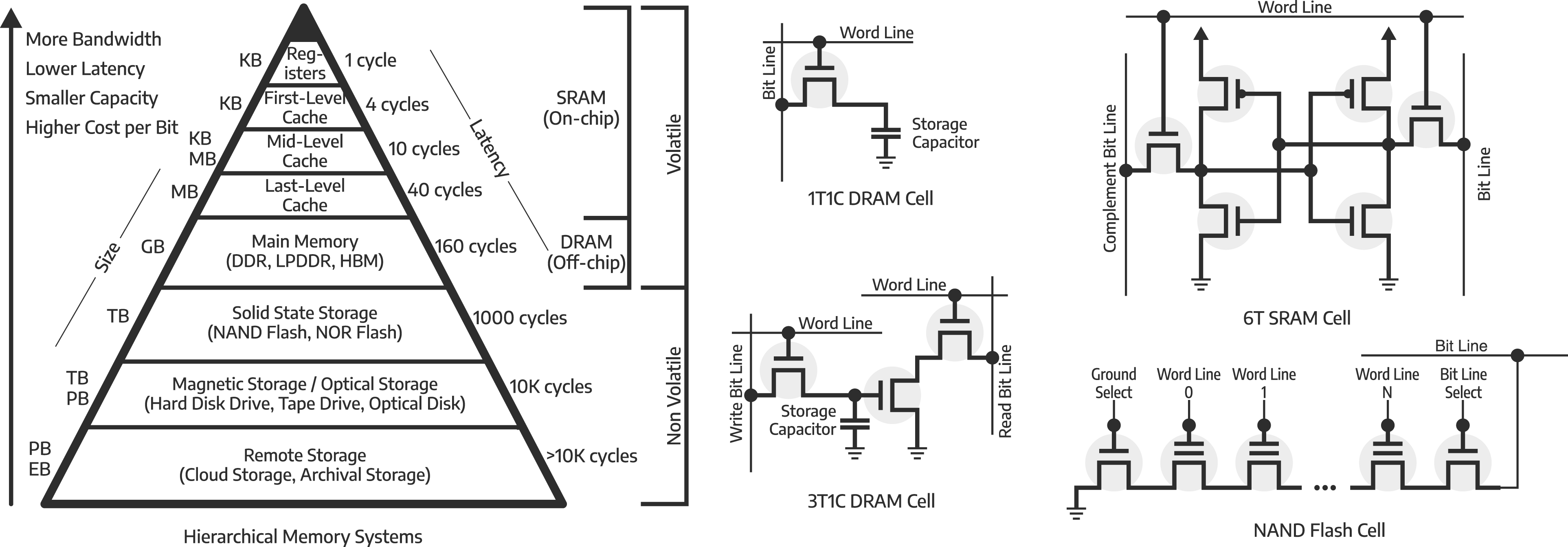
The top-half of the pyramid (Figure 1) uses volatile memory technologies (Valero et al., 2012), which require continuous supply of power to retain data (Dao et al., 2021). The bottom-half of the pyramid uses non-volatile memory technologies and can retain data in the absence of power. Volatile memory technologies directly impact performance and energy consumption (Li et al., 2019a), as they are used to store hot data 3 . They must keep up with demands from the processing units. Non-volatile memory technologies are typically used to store cold data 4 and usually have a smaller impact on the performance of the whole computer system.
In this section, we review key memory technologies, and describe their performance characteristics. Specifically, we review static random-access memory (SRAM), dynamic random-access memory (DRAM), and near-memory processing (NMP) and processing-in-memory (PIM). Finally, non-volatile memory (NVM) and storage systems are also highlighted.
Static random access memory (SRAM)
SRAM is on-chip storage, and is a building block for registers and cache memory (Liang and Wang, 2016; Mahanta et al., 2022; Zhang et al., 2020a). It is implemented by employing similar transistors (and therefore, the same process node technology) that are being used for computing units (Huang et al., 2018; James, 2009; Lage et al., 1996). The standard form of SRAM consists of six transistors 5 (6T SRAM) (Guo et al., 2005; Margala, 1999; Weste and Harris, 2010), as shown in the right-most part of Figure 1. This structure allows for fast data reading and writing, while not requiring periodic refresh, hence named static RAM (Weste and Harris, 2010).
Registers and cache memory are key components that rely on SRAM technology, and will be discussed next. Using SRAM in hardware-accelerators (Part I: Specialized and custom hardware (Hanindhito et al., 2026)) is also popular due to the lower access latency and higher bandwidth it provides (at the expense of being less energy-efficient); integration of SRAM with the silicon die is also easier, compared to DRAM and HBM. We end this part by outlining different options for programming SRAM.
Registers
Registers are very fast storage elements, close to the functional units 6 of a microprocessor (Balasubramonian et al., 2001; Cruz et al., 2000a). Registers can be as fast as the microprocessor, being able to read and write in one clock cycle (Cruz et al., 2000b; Kim and Mudge, 2003), and are responsible for storing the operands and intermediate results of instructions that are being executed. While registers are fast and favorable, microprocessors can only have a limited number of them due to limited available space around the functional units and its latency constraints 7 (Kondo and Nakamura, 2005; Mittal, 2017). GPUs have a larger size of registers due to supporting a massive number of threads 8 (Gebhart et al., 2012), where each thread has its own register allocation 9 . Part I Tables 6 and 7 (Hanindhito et al., 2026) show trends of register size in NVIDIA datacenter GPUs, where it has stayed flat at 256 kB per Streaming Multiprocessor (SM) since 2013. With this limited number of registers, applications that have a large number of intermediate results do experience register spilling (Chaitin, 2004; Nuth and Dally, 1995). This results in data being moved back-and-forth between the registers and the first level of cache (Li et al., 2016; Vizitiu et al., 2014), causing delays.
Caches
Fundamental functions
Cache is a fast, hardware-managed, on-chip memory. It is used to store commonly-used data to reduce off-chip memory access latency and bandwidth demand. Cache memory operates according to temporal and spatial locality (Lee et al., 2000). While cache operations are typically managed by hardware, understanding this process helps computational scientists develop hardware-aware algorithms 10 , leading to improved performance (Christiaens et al., 1999; Cucchiara et al., 1999; Günther et al., 2006).
Data needed by a microprocessor for the first time should be accessed from off-chip memory, which incurs high access latency and energy consumption 11 . The data will then likely reside in cache for a short period of time in case the microprocessor needs to access that data again. When the data is not used for a while, it will be evicted to a higher-level cache, and, eventually, to off-chip memory 12 (Ghandeharizadeh et al., 2015). If the microprocessor needs to access this data again, it has to be fetched from higher-level caches or off-chip memory again 13 . Temporal locality relies on the idea that, most likely, recently-accessed data will need to be accessed again. Therefore, storing that data in cache saves energy, and improves performance. Spatial locality in caching suspects neighboring data of a recently-accessed data likely need to be accessed soon (Gu et al., 2009). For instance, when an element of an array is accessed, elements adjacent to the aforementioned element likely need to be accessed in the near future, and thus are brought to the cache as well.
Algorithms that exhibit temporal and spatial 14 locality (Wolf and Lam, 1991) can lead to higher performance (Kandemir et al., 1999), and lower energy consumption (Sardashti and Wood, 2013), since they need to access off-chip memory less frequently.
Hierarchical structure
Modern microprocessors employ multiple levels of cache (Liu, 1994). Compared to the registers, the first-level (L1) cache is located farther away from the functional units; therefore, it enjoys larger capacity at a slightly higher access latency (Torres et al., 2004). L1 cache is usually private to each core (Maurice et al., 2015) and stores the most-recently-used data, as well as data due to register spilling (Li et al., 2016). General-purpose microprocessors have around 64 kB of dedicated L1 cache per core, while GPUs typically have around 256 kB of L1 cache per Streaming Multiprocessor (SM).
In addition to limits posed by physical space, the L1 cache size is kept small since a larger cache entails larger access latency 15 (Hijaz et al., 2013). It is preferred to have a fast L1 cache, instead of a large L1 cache, since it should keep up with the speed of the registers (Huang and Nagarajan, 2014).
The last-level cache (LLC) is usually shared between cores of a microprocessor (Cataldo et al., 2016), and thus, is located outside of the core complex. It interfaces directly with off-chip memory 16 (Chaudhuri et al., 2019), provides a data-sharing mechanism between cores (Albericio et al., 2013), and can have a capacity of a few hundred megabytes, albeit at a higher access latency 17 . Between the L1 cache and LLC, there can be multiple mid-level caches (e.g., L2), which balance capacity and latency between the L1 cache and LLC (Chishti et al., 2005; Wang and Lee, 2008).
Specialty cache
Microprocessors may feature specialized caches whose structure is optimized for particular memory access patterns. In general-purpose microprocessors (Part I: General-purpose microprocessors (Hanindhito et al., 2026)), a separate instruction cache (e.g., L1-I) is used to cache the program instructions in addition to the first-level data cache (e.g., L1-D) that is used to store most-recently-used data. The instruction cache is read-only, while the data cache is capable of read and write. The split design has some advantages: (a) it doubles the aggregate bandwidth of the first-level cache, since there are two physical caches (McFarling, 1989; Smith, 1982); (b) it lowers the access latency, since the instruction cache can be physically placed near the instruction-fetch-and-decode unit, whereas the data cache can be placed near the memory unit (Smith, 1982); and (c) most importantly, it avoids interference 18 between instructions and data, since they have different access patterns (Racunas and Patt, 2003; Trancoso, 2005).
In GPUs (Part I: GPU memory system (Hanindhito et al., 2026)), in addition to the data caches (i.e., L1 and L2), there exists read-only texture cache, and read-only constant memory cache. Texture cache is optimized to store large amounts of data with spatial locality, with support for hardware filtering and interpolation, which is mostly beneficial for graphics applications. The constant memory cache is used to store small amounts of constant data (e.g., pre-computed constants), and provides lower access latency than texture cache.
Coherency
Coherency among the cache hierarchies needs to be maintained: if data is changed in the lower-level cache, it should be reflected in the higher-level cache, as well as in the off-chip memory (Ros et al., 2015). Consider a core modifying data in its private lower-level cache; if another core needs to access this modified data, it can obtain the data from the shared last-level cache, which should contain the correct version of the data after being modified by another core.
Cache coherency becomes more complex in multi-core microprocessors and massively-parallel architectures (e.g., GPUs) (Joshi and Ramasubramanian, 2015; Martin et al., 2012; Parvathy et al., 2016): it requires expensive hardware structures that consume additional area and power to track vast amounts of in-flight coherence requests, introduces excessive coherence traffic overheads that degrade performance, and complicates program execution through additional transient states and communication classes (Keckler et al., 2011; Singh et al., 2013). Accordingly, massively-parallel architectures do not support cache coherency 19 , and this responsibility is delegated to the programmer.
User-managed vs. compiler-managed scratchpad memory
While general-purpose processors rely on hardware to manage SRAM in the form of cache, several hardware architectures allow users or compilers to manage the on-chip SRAM explicitly. Some algorithms may have memory access patterns that cause cache trashing (Jaleel et al., 2010; Seshadri et al., 2012), reducing the effectiveness of the cache, and resulting in significant performance degradation. In these situations, explicit management of on-chip memory may improve memory access performance.
User-managed shared memory in GPUs provides this opportunity (Part I: GPU memory system (Hanindhito et al., 2026)). Some GPU architectures 20 have both L1 cache and shared memory implemented as unified on-chip memory. This provides flexibility to the users in sizing the shared memory, leaving the rest for L1 cache. Therefore, using shared memory effectively reduces the size of the L1 cache (Part I Tables 6 and 7 (Hanindhito et al., 2026)).
Management of the on-chip SRAM by a programmer often requires a deep understanding of the underlying algorithm and its memory-access pattern. If not done correctly, it may lead to performance loss, especially in unified architectures such as GPUs, where it affects the smaller L1 cache, which may outweigh performance gains achieved through using the shared memory.
Using compilers to manage SRAM, e.g., on hardware accelerators, is becoming more common. For instance, the only available memory on Cerebras’ Wafer Scale Engine (WSE) is SRAM 21 (Lauterbach, 2021; Lie, 2022) (Part I: Specialized and custom hardware (Hanindhito et al., 2026)), which consumes 50% of the total chip area. WSE relies on a compiler to optimally distribute the data across the SRAM.
Dynamic random access memory (DRAM)
DRAM is an off-chip 22 memory that provides more capacity, and is more energy-efficient, compared to on-chip SRAM (Hassan, 2018), at the expense of being slower. DRAM is implemented with a different technology than the logic circuits that implement the processing units (Iyer and Kalter, 1999) and is connected to the microprocessor through an external bus. Classic DRAM was implemented by using three transistors and one capacitor (3T1C), while the most common implementation uses one transistor and one capacitor (1T1C) (Gong and Chung, 2016) (middle of Figure 1). The presence or absence of a charge stored in the capacitor represents bit 0 or bit 1. This structure allows DRAM to have a significantly higher bit density compared to SRAM, and thus lowers the cost per bit (Si et al., 2021).
Unlike SRAM, since the charge in the capacitors fades over time (Gong and Chung, 2016), DRAM needs to be refreshed periodically to maintain data integrity (Nair et al., 2014). Hence, it is named dynamic RAM. The periodic refresh occurs every few microseconds, depending on the manufacturing technology and bit density 23 (Nguyen et al., 2019). During the refresh, the data is read by the sense amplifier (Blalock and Jaeger, 1992) through sensing the charge in the capacitor. Next, the same data is written back, by putting the correct amount of charge in the capacitor. As the bit density and speed of DRAM increase, so do the negative impacts of periodic refresh on performance and power consumption 24 (Baek et al., 2014; Nguyen et al., 2019). In addition, read operations in DRAM are destructive: reading a memory cell destroys its content, and thus, rewriting after reading is required. It is worth mentioning that 3T1C implementation of DRAM 25 does not exhibit this issue (Jacob et al., 2007). Nevertheless, the 1T1C implementation is preferred due to its higher bit density (Yin et al., 2019).
In the remainder of this part, we review how DRAM evolved through the years, graphics DRAM, High-Bandwidth Memory, and the main technological challenge DRAM faces.
Classic DRAM
The first commercially-available DRAM chip was Intel 1103 (1970) (Dennard, 2018), with 1024 bits capacity
26
on a 10 mm2 die size (Klein, 2016). It cost a penny per bit (Santo, 1988), the same as the magnetic-core memory, which was a technology it replaced. At Intel 1103 capacity, the magnetic-core memory would have had a square-foot footprint, and a pound of weight (Lojek, 2007). DRAM’s success in replacing the magnetic-core memory fueled the development of larger and higher-speed DRAMs (Figure 2). The top half of Figure 2 shows trends related to important metrics in DRAM: (a) the process node with which the DRAM chip is manufactured; (b) the chip bit capacity; and (c) the pin transfer rate, which measures how fast the DRAM chip transfers data through each of its pins. DRAM chip capacity has increased through the years: it roughly doubled every 2.5 years due to smaller process nodes. However, its growth slowed down in the late 1990s due to the technological challenges highlighted in Main technology challenges. The data transfer rate, expressed as the pin transfer rate, has steadily increased to satisfy the need for even higher bandwidth; however, there is a trade-off between chip capacity and pin transfer rate, as discussed in Graphics DRAM. The bottom half of Figure 2 shows the progression of DRAM standards
27
in industry. Evolution of Dynamic Random Access Memory (DRAM) since the 1970s, with projections until 2030.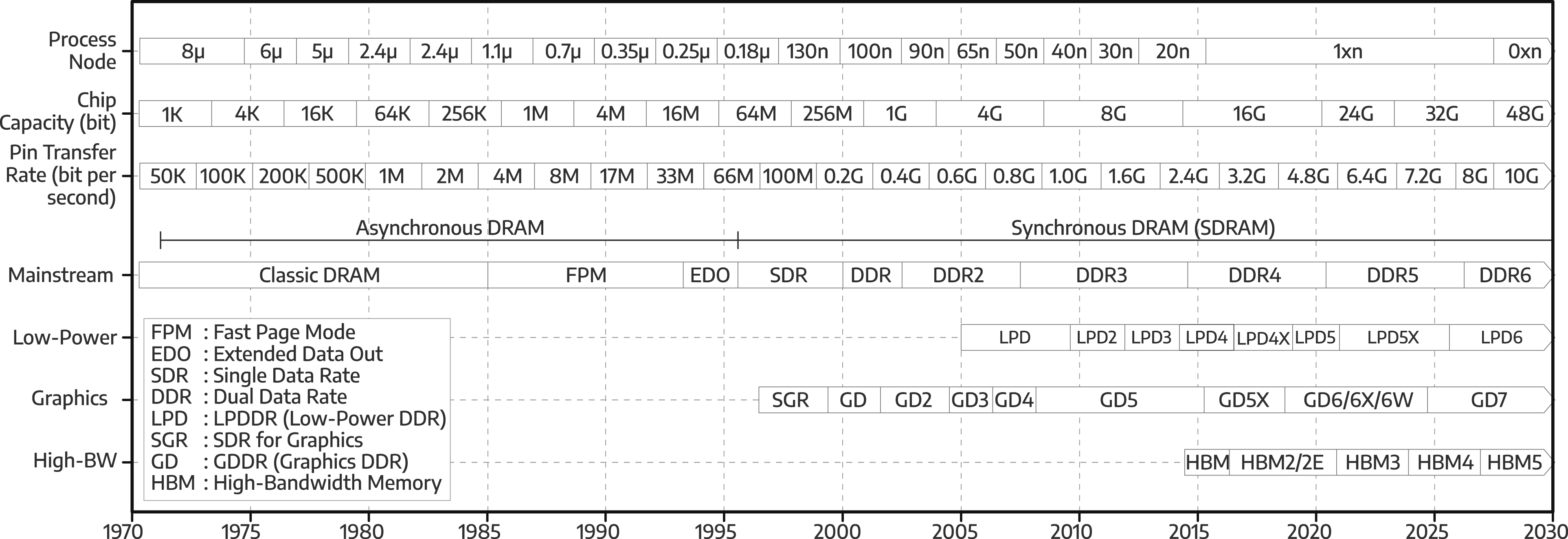
Fast page mode and extended data out DRAM
During the mid-1980s, the DRAM interface, which connects a microprocessor into the DRAM modules containing multiple DRAM chips, could not keep up with the demands of microprocessors (Jacob et al., 2007). Performance improvement of microprocessors (Part I Figure 5 (Hanindhito et al., 2026)) significantly outpaced that of DRAM. This led to several innovations in DRAM chip development, aimed at reducing latency, and increasing bandwidth (Jacob et al., 2007).
The Fast Page Mode (FPM) DRAM, and the Extended Data Out (EDO) DRAM, improved bandwidth over classic DRAM implementations. In classic DRAM, to request specific data, a row 28 in the memory array is selected (“opened”) by using the row address. The data represented as electrical charges are then propagated to the sense amplifiers, where they are translated to digital (binary) data. Then, through the column address, the requested data is selected and put into the output pins. This lengthy process must be repeated, even if the next requested data is located on the same row. FPM DRAM 29 and EDO DRAM 30 made DRAM transactions more efficient. We refer to (Jacob et al., 2007) for details. These improvements required small modifications to the structure of DRAM. Nevertheless, they improved system performance by as much as 30% (Cuppu et al., 1999a, 2001).
Mainstream synchronous DRAM
Classic DRAM, FPM DRAM, and EDO DRAM, used asynchronous interfaces between the DRAM chips and microprocessors. The asynchronous design has been primarily motivated by analog circuits (i.e., sense amplifier) in DRAM. Since the duration of operations in DRAM varies (based on different designs, process variations, and specific manufacturer), they are measured in nanoseconds, instead of number of cycles. Therefore, at the time, it was more challenging to tie DRAM’s operations with the processor’s clock. This asynchronous interface caused control signals of the memory controller 31 , and the requested data from the DRAM chips, to arrive at DRAM pins and microprocessor pins at non-deterministic times. Accordingly, transaction events between the memory controller and DRAM chips were temporally unpredictable, making bandwidth and latency improvements challenging. Specifically, lack of synchronization and not using a common-time-reference, on the interface between the microprocessor and DRAM, makes maintaining the correctness of the transaction difficult. The microprocessor has to “wait” for the previous instruction to be completed by the DRAM chips, before issuing another instruction. The window in which the microprocessor needs to wait, typically expressed in nanoseconds, varies greatly 32 , which incurs a performance penalty, limiting the achievable bandwidth and latency. Synchronous interfaces tried to address these challenges.
During the mid-1990s, DRAM started to use synchronous interfaces (Cosoroaba, 1995), where a clock signal is used to control the timing of the transactions (i.e., through the use of state machines), leading to predictability. Accordingly, DRAM speed was expressed through clock cycles, as opposed to nanoseconds (Cuppu et al., 1999a). In a synchronous interface, the transaction time is known due to using a common time reference 33 , allowing the microprocessor to issue another instruction before the completion of the previous instruction 34 . The microprocessor may also issue multiple instructions to different DRAM modules 35 , provided that it obeys the timing requirements of the DRAM chips (Jacob et al., 2007).
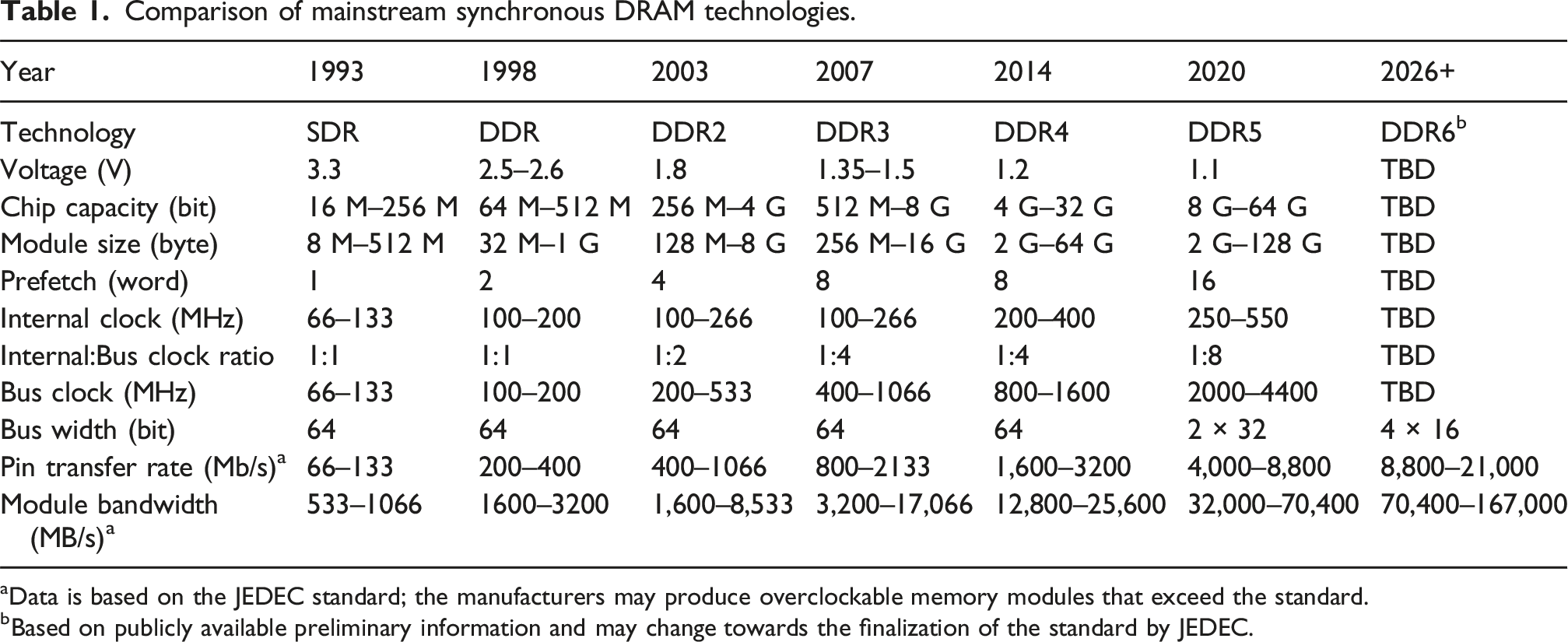
Moving from asynchronous to synchronous interfaces in the early version of synchronous DRAM (SDRAM) incurred significant implementation costs, with almost no performance gains, compared to EDO DRAM (Jacob et al., 2007). However, it provided a strong foundation for future SDRAM developments for decades to come (Table 1). We highlight the main synchronous DRAM technology developments next.
Single data rate (SDR)
Single Data Rate (SDR) SDRAM (1993) was the first generation of SDRAM, where the DRAM chips operated at a voltage of 3.3 V, and had a bus clock frequency of 66 MHz (PC66), 100 MHz (PC100), or 133 MHz (PC133) (Davis et al., 2000; Jahed, 1995). With this bus clock frequency, SDR could carry data at a rate of 66 Mb/s to 133 Mb/s for each module pin.
An SDR module, called Dual In-Line Memory Module (DIMM) (Cuppu et al., 1999b; Rixner, 2004), had 64 data lanes, which were connected to the microprocessor’s memory controller. Hence, it could send a word of 64 bits (8 bytes of data) in each clock cycle, translating to a module bandwidth of 533 MB/s 36 to 1066 MB/s.
Comparison of mainstream synchronous DRAM technologies.
aData is based on the JEDEC standard; the manufacturers may produce overclockable memory modules that exceed the standard.
bBased on publicly available preliminary information and may change towards the finalization of the standard by JEDEC.
Double data rate (DDR)
Succeeding SDR technologies focused on improving the interface bandwidth. Instead of transferring 64 bits (8 bytes) of data at each clock cycle, Double Data Rate (DDR) SDRAM (Cosoroaba, 1997) was able to read and write two words of 64 bits (16 bytes of data) during each clock cycle (Davis et al., 2000). This was realized by using both the rising and falling of the clock edges, which effectively doubled the bandwidth.
In this generation, DRAM chips had a lower voltage of 2.5 V (Yoon et al., 1999b), allowing for reduced power consumption per bit, and higher bit capacity per chip within the same power envelope 38 , with up to 1 GB of module size.
With the double prefetch 39 length, at 200 MHz of bus clock, and 64-bit module interface, the DDR module can achieve 3200 MB/s 40 of memory bandwidth, which is twice that of SDR (Yahata et al., 2000).
DDR2
Compared to DDR, DDR2 (Kyung et al., 2005) doubled the bus clock, without doubling the internal clock of the DRAM chips, which, effectively, doubled the bandwidth, but did not improve latency. To do so, DDR2 doubled the prefetch into four words (Shuang-yan et al., 2005). Since the internal clock is half the frequency of the bus clock (Prince, 2003), the latency 41 of the DDR2 module was higher than that of the DDR 42 .
The voltage was reduced to 1.8 V, with a significant increase in DRAM chip bit capacity, which was enabled by using advanced process nodes (Prince, 2003). This allowed implementation of 8 GB DIMMs, with expected module bandwidth that could reach 8533 MB/s 43 .
DDR3
To further increase bandwidth, a similar approach was followed by DDR3 (Fujisawa et al., 2007; Park et al., 2005), which doubled the prefetch bandwidth to 8 words, reduced the voltage 44 to 1.5 V, and doubled the chip bit capacity to allow 16 GB of DIMM size (Cui et al., 2008; Fujisawa et al., 2007).
DDR4
DDR4 (Koo et al., 2012; Shim et al., 2018) supports even higher DRAM chip bit capacity, at higher bus clock frequency (Lingambudi et al., 2016), while retaining the same prefetch width as DDR3 (Islam et al., 2014). Therefore, the DRAM chips need to interleave read and write from several bank groups to keep the bus busy (Islam et al., 2014; Sohn et al., 2013).
DDR5
The latest standard, DDR5 (Kim et al., 2019; Winterberg et al., 2023), doubles the prefetch width to 16 words (Kim et al., 2020) to reach higher bandwidth while maintaining internal clock frequency around 250 MHz to 550 MHz. It splits the bus into two 32-bit sub-channels to increase parallelism (Liu et al., 2023) and achieves up to 70.4 GB/s of module bandwidth.
DDR6
DDR6 is the successor to DDR5, slated to launch between 2026 and 2027 or even later. It doubles the number of sub-channels to four 16-bit subchannels and is expected to double the bandwidth provided by DDR5 at lower voltage. Although it was rumored to use PAM-4 modulation, JEDEC most likely will keep using the NRZ due to the complexity of the PAM-4 (Part I: Signal coding and modulation (Hanindhito et al., 2026)). In addition, a new module form factor called Compressed-Attached Memory Module (CAMM) will be introduced to replace the aging DIMM, accommodating the signal integrity challenge with the anticipated increase in the bus clock. JEDEC standardized CAMM for DDR5 in 2023 with limited adoption.
Mobile and low power DRAM
Mobile devices use the low-power version of DRAM chips, referred to as Low-Power DDR-SDRAM (LPDDR). The LPDDR chip is usually placed very close to the processor (Hollis et al., 2019), either by soldering the chip closer to the microprocessor, or by putting the LPDDR chip on top of the microprocessor package (i.e., package-on-package (Hsieh, 2016; Lin et al., 2014)). The connection between LPDDR and the processor has a small bus width 45 . This integration technique, and the smaller bus width, reduces the wire resistance, which reduces power consumption.
To further reduce power consumption, LPDDR operates on a lower voltage (Hajkazemi et al., 2015), compared to the standard DRAM: 1.8 V on LPDDR, 1.2 V on LPDDR2 (2009) and LPDDR3 (2012), 1.1 V on LPDDR4 (2014), and 0.6 V on LPDDR5 (2019) and LPDDR5X (2021). Moreover, the periodic refresh operations are optimized by applying multiple techniques that control power consumption aggressively (Baek et al., 2014; Hemani and Klapproth, 2006). LPDDR’s lower power consumption is attractive to data centers and high-performance computing clusters. For instance, LPDDR5X is used for the Grace CPU memory in NVIDIA Grace-Hopper (GH200) and Grace-Blackwell (GB200) (Tirumala and Wong, 2024) CPU-GPU heterogeneous platforms.
Graphics DRAM
GPUs that rely on high-bandwidth memory often need different approaches for designing the DRAM chips, along with tighter integration of memory with the device.
Higher bandwidth for memory can be achieved through: (a) constructing a wider memory bus (Kim et al., 2014; Li et al., 2018); (b) increasing the bus clock frequency (Cho et al., 2012); (c) running DRAM chips at a higher internal clock frequency (Woo, 2010); and (d) utilizing denser signal modulation (Part I: Signal coding and modulation (Hanindhito et al., 2026; Horowitz et al., 1998; Wang and Buckwalter, 2011) between the microprocessor and DRAM chips. In what follows, we review how the memory bandwidth of GPUs has increased over the years through the evolution of various technologies.
Evolution of graphics memory technology
Earlier DRAM for GPUs was constructed by using video RAM (VRAM) to satisfy the bandwidth requirements at the time (Prince, 1999). VRAM is an ancestor of SDRAM, which comprised multi-ported 46 asynchronous DRAM, and serial access memory (SAM). This allowed VRAM to operate as an asynchronous DRAM in one port, while having a synchronous serial memory interface in another port.
In 1997, GPUs started to use Synchronous Graphics Random Access Memory (SGRAM), which was derived from the Synchronous DRAM (SDRAM), eliminating the need for more expensive, multi-port asynchronous DRAM (Prince, 1999).
The successor of SGRAM is Graphics Double Data Rate SDRAM (GDDR-SDRAM, which was initially known as DDR-SGRAM (Foss, 1997; Prince, 1999)). It was based on the Double Data Rate SDRAM (DDR-SDRAM) (Cosoroaba, 1997). The GDDR-SDRAM chip is specifically designed to run at higher internal clock frequencies, compared to mainstream DRAM. To do so, it sacrifices bit capacity per chip 47 (Dunning et al., 2009), by adding more periphery components, which facilitate faster memory transactions. The increase in internal clock frequency of GDDR chips requires more cooling, as they dissipate more heat compared to mainstream DRAM chips.
Comparison of graphics synchronous DRAM technologies.
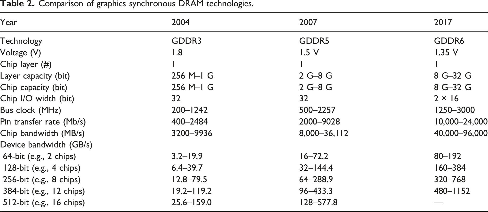
The GDDR6X (2020) (Hollis et al., 2022) can 50 provide triple the bandwidth of GDDR5 51 through using the same bus width, but by using a higher bus clock frequency, and denser signal modulation 52 . With their higher internal clock frequency, denser signal modulation, and higher bus clock frequency, GDDR6X chips run at junction temperatures 53 exceeding 100°C. The high temperature is concerning to some users, since it may impact the longevity of their products 54 . Unlike GDDR6X, next-generation GDDR7 uses PAM-3 instead of PAM-4 modulation to reduce costs, complexity, and power while delivering a meaningful increase in pin data rate over GDDR6. GDDR7 was launched in early 2025 with the launch of consumer-class NVIDIA Blackwell GPUs.
Integration of memory with GPUs
GDDR chips are closely integrated with GPU (Kim et al., 2016; Li et al., 2018) (Figure 3). This allows GDDR chips to run at higher bus clock frequencies, and use denser signal modulation. However, parasitic capacitance from the printed circuit board (PCB) materials
55
, and interference between adjacent wires
56
, become more severe at higher frequencies and longer distances (Part I: Wiring, connectivity, and signal integrity (Hanindhito et al., 2026)). Therefore, to achieve higher bus clock frequencies, and to use denser signal modulation, the distance between the GPU chip and GDDR chips must be minimized. Typical placement of a GPU with a 384-bit memory bus, when connected to GDDR5 chips, is shown on the left-side of Figure 3, whereas the typical placement of a GPU with 384-bit memory bus, when connected to GDDR6X chips is shown in the middle of Figure 3. Evolution of DRAM interface on GPU, where providing higher bandwidth is the main design objective. NVIDIA GeForce GTX 980Ti has 338 GB/s memory bandwidth, implemented by using 12 chips of GDDR5 memory, each having a 32-bit bus width, resulting in a total of 384-bit bus width. The newer NVIDIA GeForce RTX 4090 uses 12 chips of GDDR6X memory with the same total bus width of 384-bit. With a significantly faster bandwidth of 1 TB/s coming from its higher effective transfer rate, the memory chips must be placed as close as possible to the GPU package to maintain signal integrity. Finally, High-Bandwidth Memory (HBM) provides a wider memory bus of 1024-bit per chip (i.e., HBM stack) to achieve significantly higher memory bandwidth. Implementing this wide memory bus on printed circuit board (PCB) is challenging. Therefore, HBM die is usually placed on the same package that the GPU resides on through using a silicon interposer (e.g., in NVIDIA A100 GPU), as explained in Part I: Advanced packaging technologies (Hanindhito et al., 2026).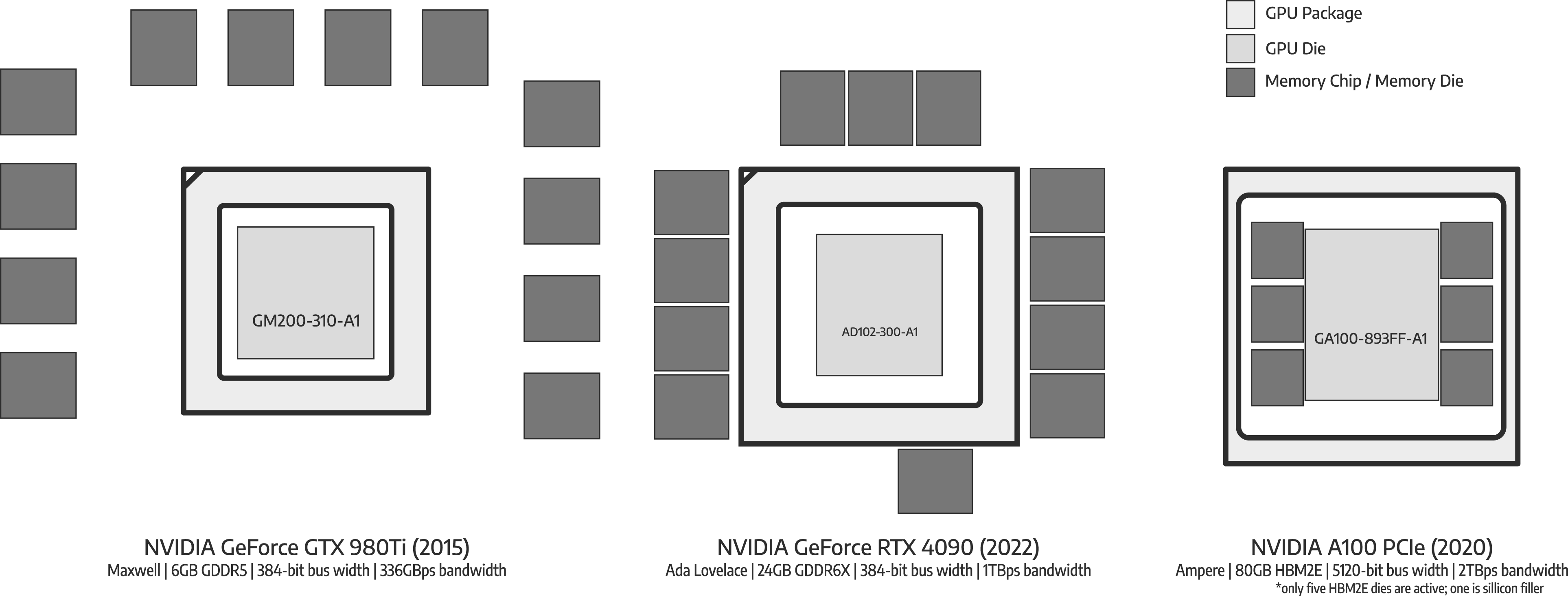
Increasing the memory bandwidth can also be realized by widening the bus (Mahapatra and Venkatrao, 1999), through adding more GDDR chips, and more memory channels. For instance, a low-end GPU can have a 64-bit bus-width, consisting of two GDDR chips, whereas a high-end GPU can have a 512-bit bus, consisting of as many as 16 GDDR chips.
Manufacturing a wider bus is challenging, since it requires routing more signal paths on a PCB (Na et al., 2017; Nitin et al., 2018). Each bit line on the memory bus becomes a single wire on the PCB. Each wire carries a high-frequency signal, and thus, can interfere with neighboring wires, which then affects data integrity (Part I: Wiring, connectivity, and signal integrity (Hanindhito et al., 2026)). Therefore, to realize a wider memory bus, new technologies that overcome the physical limitation of PCB are needed.
High-bandwidth memory (HBM) and variants
Advances in packaging technologies (Part I Figure 6 (Hanindhito et al., 2026)) allow DRAM dies to be stacked on top of each other, and then be placed on the same package that a GPU resides (the right-side of Figure 3) (Loh et al., 2015). Instead of using wires that are implemented on PCB to connect a GPU to the stacked DRAM chips, a silicon interposer (Part I: Advanced packaging technologies (Hanindhito et al., 2026)) is used (Cho et al., 2015; Lee et al., 2015b). Each stack of the DRAM chips can have a bus width as wide as 1024 bits (Kim, 2015; Martwick and Drew, 2015), which is 32 times wider than the bus width of GDDR chips. This makes implementation of a wider memory bus at lower interconnect power dissipation possible (Zhao et al., 2017). Examples of on-chip bus topologies (Pasricha and Dutt, 2010): (a) The single bus is the simplest and cheapest on-chip bus topology. All masters share the bus as the communication channel for all transactions with the system’s slaves and only one master can have access at a time. The performance of the single bus does not scale with the number of components, due to increased traffic and congestion, where arbitration can lead to the starvation of some masters. (b) In the full bus crossbar, a dedicated bus is used for each possible master-slave connection. This corresponds to the highest possible system performance, as it maximizes the theoretical onchip communication bandwidth. Arbitration logic is now required for each slave, rather than for each bus. However, it becomes prohibitively expensive as the number of system components increases, adversely affecting area, cost, power consumption and routing complexity. (c) The partial bus crossbar is a mixture of the single bus and full bus crossbar. Essentially, it trades off the performance of the full bus crossbar for a reduction in area, cost and power consumption.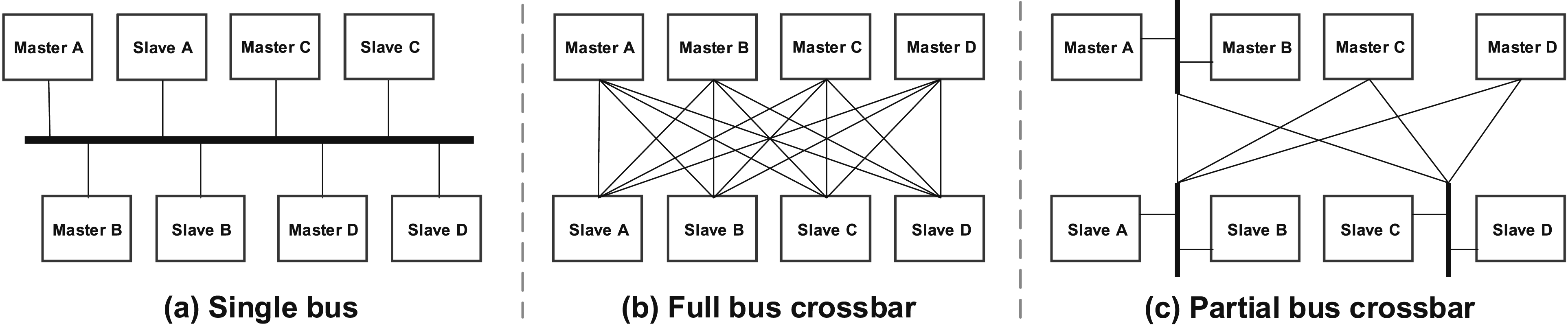
Comparison of high-bandwidth synchronous DRAM technologies.
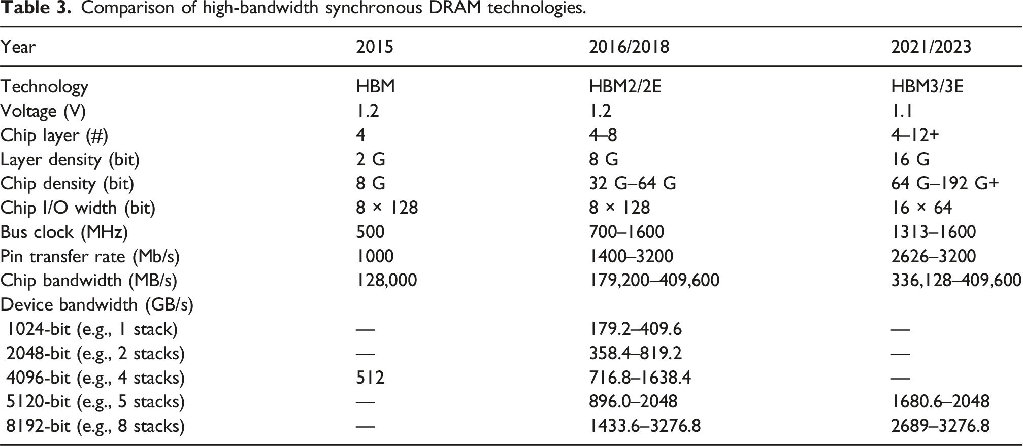
The first-generation 57 HBM (2015) can stack up to 4 DRAM dies, enabling 8 Gb chip capacity (Lee et al., 2015a; Macri, 2015). HBM2 (2016) (Cho et al., 2018) and HBM2E (2018) (Chun et al., 2021; Lee et al., 2020b) increased the number of DRAM dies to 8, realizing 64 Gb of chip capacity, while maintaining the same 1024-bit bus interface. The latest generation, HBM3 (2021) (Park et al., 2023; Ryu et al., 2023), increases the number of stacked DRAM dies to 12, with the possibility of having 16 stacked DRAM dies in the future, pushing the chip bit capacity beyond 192 Gb. Its successor, HBM3E, was launched in 2024.
Stacking more DRAM dies into the HBM increases the chip memory capacity. However, the parasitic capacitance of thru-silicon vias (TSV), which connects each layer of the stack, becomes more problematic, as the stack size grows (Farmahini-Farahani et al., 2018; Kim et al., 2021e). Moreover, stacking more DRAM dies on the chip makes thermal dissipation of HBM chips more challenging, as the surface area of the chips remains the same (Kim et al., 2023; Lee et al., 2023b). Therefore, the next generation of HBM, HBM4 (2025+), is expected to have a vapor-chamber cooling system, which is a cooling technology that is often used for chips that need high thermal dissipation. Moreover, HBM5 (2027+) is expected to have a micro-channel cooling system.
Despite the above challenges, HBM has been successful in fulfilling the demand for memory bandwidth of high-end GPUs. However, high manufacturing costs and low production capacity (Jun et al., 2017; Abdennadher et al., 2018) limit the adoption of HBM to data center class products, leaving the consumer market with GDDR.
In addition to GPUs, HBM has been used in many other devices that need high-bandwidth memory. For instance, Intel Knights Landing, a manycore architecture (Part I: Many-core processors (Hanindhito et al., 2026)), features 16 GB Multi-Channel DRAM 58 (MCDRAM) (Pohl and Sattler, 2018; Sodani, 2015), which was derived from HMC (Jeddeloh and Keeth, 2012). In addition, Intel Xeon Max 59 features (on-package) 64 GB HBM2E (Biswas, 2021), providing considerable amount of memory bandwidth. This can especially benefit applications that fit into the HBM. In both cases, conventional (off-package) DDR5-SDRAM is still provided to make up for the limited capacity of HBM, which can be configured in multiple ways. HBM is also used in FPGAs (Holzinger et al., 2021; Shi et al., 2022), CGRAs (Kim et al., 2017), and ASICs (Jouppi et al., 2020, 2021) (Part I: Specialized and custom hardware (Hanindhito et al., 2026)).
Main technology challenges
As DRAM moves to more advanced process nodes, the chip bit density increases. This makes larger-capacity memory modules possible, and drives down cost-per-bit. However, DRAM is facing difficulties in moving to more advanced process nodes: it has stagnated in the 1x nm process node 60 (Kang et al., 2014; Mellor, 2020; Shiratake, 2020) for almost a decade, and is expected to remain in this range for the foreseeable future (Chen et al., 2023b).
The structure of DRAM is the main cause of this difficulty: DRAM uses a capacitor to store a charge for representing bit 0 and bit 1. While more advanced process nodes have enabled transistor shrinking, capacitor shrinking remains challenging. As a capacitor becomes smaller, the electrical charge it can hold is also reduced (Chen et al., 2023b). Eventually, it becomes difficult for the sense amplifier to detect the charge (Shiratake, 2020). Additionally, due to the smaller charges that capacitors can hold, they need to be refreshed more frequently, reducing DRAM’s performance (Khan et al., 2014; Liu et al., 2013). Moreover, as the bit density of DRAM becomes larger, the smaller charge has to travel through longer wires in DRAM chips, making it difficult to maintain data integrity (Part I: Wiring, connectivity, and signal integrity (Hanindhito et al., 2026)).
Due to these challenges, development of next-generation DRAM technologies is costly. Indeed, there are only three major players 61 in the DRAM industry, due to its reliance on large research and development budgets.
Near-memory processing (NMP) and processing-in-memory (PIM)
Centralized memory and compute units are separated from each other in the von Neumann architecture, which constitutes the vast majority of modern computing systems. The interface between the compute unit and off-chip memory has limited bandwidth, and often becomes the bottleneck in overall system performance. In addition, excessive data-movement consumes a lot of energy 62 . Near-memory processing (NMP) and Processing-in-memory (PIM) attempt to address the von Neumann bottleneck and reduce energy consumption by bringing the compute units closer to where data is stored (Khoram et al., 2017; Mutlu et al., 2019). With their promising performance and reduced energy consumption, NMP and PIM are attractive for data-intensive workloads. Nevertheless, these technologies are still in their infancy. A better software stack 63 is also critical for the adoption of these technologies by the end users (Ghose et al., 2019).
Near-memory processing (NMP)
The NMP brings the compute units near the memory arrays. Accordingly, the compute units and memory arrays can be integrated at chip or package levels. The capability of the compute units depends on their size. Usually, when the compute unit is placed on the same die where the memory arrays are implemented, there is competition for space, which typically results in simpler compute units. Next, we highlight a few examples that use NMP.
Cerebras and SambaNova
Cerebras’ Wafer Scale Engine and SambaNova’s Reconfigurable DataFlow Unit (Part I: Specialized and custom hardware (Hanindhito et al., 2026)) distribute arrays of on-chip memory units (SRAM) and arrays of compute units throughout the chip. This design enables interaction of memory and compute units with very high bandwidth.
UPMem
UPMem (Devaux, 2019) develops NMP through integrating compute units within the same die that a DRAM memory array resides on, referred to as DRAM processing units (DPUs 64 ). Since both the compute and memory units are implemented on the same die, the compute logic has to be manufactured by using the same process node technology that is used for DRAM cells. This leads to a suboptimal design, since the logic circuits could have been implemented with a smaller process node technology otherwise. Nevertheless, substantial performance improvements and energy savings are reported due to parallel operation of thousands of DPUs 65 , as well as the availability of significantly high bandwidth between the memory and compute units. Furthermore, UPMem DPU modules are drop-in replacements for standard memory modules 66 , allowing seamless transition from an existing memory technology to an NMP technology.
Samsung
Samsung released their version of NMP by integrating Programmable Computing Units (PCUs) into their High-Bandwidth Memory (HBM-PIM) and LPDDR5 (LPDDR5-PIM) (Kim et al., 2021b; 2022a). While they use PIM in naming their products, the associated technology that they use is still NMP. In addition, Samsung also released Acceleration DIMM (AxDIMM), which integrates reconfigurable logic to the standard DDR4 memory modules (Ke et al., 2022).
Processing-in-memory (PIM)
Unlike NMP that relies on separate compute units placed near the memory arrays, PIM performs the computations directly in the memory arrays. The approach varies based on the utilized memory technology. However, it usually requires minimal changes to the memory array structures, and relies on altering the memory commands issued by the memory controller to perform the computations. PIM has been implemented in different memory technologies: SRAM (Fujiki et al., 2021c), DRAM (Fujiki et al., 2021a), and Non-volatile memory 67 (Fujiki et al., 2021b).
Based on its operation, PIM can be divided into two categories: analog (Feinberg et al., 2018) and digital (Imani et al., 2019a). Analog PIM leverages inherent electrical properties of the memory arrays to perform computations according to Kirchoff’s law 68 (Zhang et al., 2020b). Analog circuits are more sensitive to noise, manufacturing variations, temperature changes, and voltage fluctuations. Moreover, inside SRAM-based and NVM-based PIM, the analog-to-digital and digital-to-analog converter blocks consume the majority of area and power of the memory chip (Talati et al., 2016). Digital PIM attempts to address this issue by performing digital logic 69 operations on the memory arrays. Through using logical operations, more complex arithmetic operations can be performed. However, this makes arithmetic operations, such as addition and multiplication, have significantly longer latency since the operands are processed bit-by-bit. Although individual arithmetic operations take longer latency, significant performance improvements result from the massively parallel operations that memory arrays of digital PIM can perform.
Examples of PIM implemented in DRAM include Compute DRAM (Gao et al., 2019) and Ambit (Seshadri et al., 2017), whereas Neural Cache (Eckert et al., 2018) is an SRAM PIM. Non-volatile memory technologies investigated for PIM include phase-change memory (Hoffer et al., 2022), resistive RAM (Hanindhito et al., 2021; Imani et al., 2019b), spintronic RAM (Chowdhury et al., 2018), and NAND Flash (Gao et al., 2021).
Non-volatile memory (NVM)
Non-volatile memory technologies enable permanent storage of data in the absence of power. Flash-based NVM is becoming more popular, not only for storing cold data, but also for storing hot data due to its higher density compared to DRAM, especially for HPC and ML applications that deal with big data. Emerging NVM technologies, such as phase-change NVM, are actively being investigated as an alternative to Flash-based NVM, which has been approaching its scaling limit.
Flash-based memory
Flash memory is an early example of NVM, and was invented in 1984 (Masuoka et al., 1984). It can be constructed by using NAND 70 Flash or NOR 71 Flash. NOR Flash has a higher random access speed compared to NAND Flash (Wong, 2010), along with a higher cost-per-bit. A NOR Flash cell 72 is 2.5× larger than a corresponding NAND Flash cell (Van Houdt, 2006). Due to its high bit density, and low cost-per-bit, NAND flash is generally preferred for manufacturing flash-based storage 73 (Lu, 2012).
We review key characteristics and technology trends in NAND Flash, and highlight how they are being used close to microprocessors to augment DRAM-provided memory capacity.
Flash memory operations
NAND flash (right of Figure 1) uses two transistors to control read and write to the cells, along with several floating-gate transistors for storing the data. Data is stored by maintaining an electrical charge in the floating gate, which is surrounded by oxide layers as insulators 74 (Friederich, 2010). Unlike the capacitor inside DRAM, the floating gate transistor can hold its charge for years, without the need for periodic refresh.
Each write operation to the cell slightly damages the oxide layers due to the high voltage needed for either pushing an electron into the floating gate, or removing an electron from the floating gate (Zambelli et al., 2010). After a sufficient number of write cycles, the oxide layers are damaged to the point where the floating gate cannot hold the charges, making the cell unusable. Therefore, unlike a DRAM cell, which has virtually no degradation (Itoh, 2011), NAND Flash 75 has a limited number of write cycles. Total bytes written (TBW), and drive writes per day (DWPD), are used as metrics to represent endurance of flash memory products (Li et al., 2019b; Woo et al., 2020). To improve endurance, manufacturers usually provide more cells than the stipulated capacity, and use them for over-provisioning to substitute failing cells with spares (Li, 2020). The flash memory controller is responsible to perform wear-leveling (Dharamjeet et al., 2022; Liao et al., 2015), by managing the use of the cells in such a way that all of them degrade with the same rate.
Miniaturization challenges
Increasing the bit density of flash memory can be achieved through transistor miniaturization. However, shrinking the size of the transistors reduces their endurance, since the oxide layers become thinner, making them more susceptible to damage (Koh, 2009). The use of floating gate transistors limits 76 future scaling of flash memory, and thus, a new cell structure, referred to as charge trap, is being used (Lu, 2012). Instead of using semiconductors as storage elements 77 , the charge trap uses dielectric layers 78 to hold the charge (Grossi, 2010). Compared to the floating gate, charge trap has lower reliability. However, due to advances in processing materials, charge trap is now preferred, especially for 3D NAND (Advani, 2016).
Multi-level cell
Bit density can also be increased by employing multi-level voltage in a cell, which can then represent more than one bit (Micheloni and Crippa, 2010). In a single-level cell (SLC) (Kouchi et al., 2020, 2021), there are only two levels of voltage, which represent bit 0 and bit 1. In a multi-level cell (MLC) (Lee et al., 2016b; Micheloni et al., 2006), there are four levels of voltage, which represent two bits, with values 00, 01, 10, and 11 (Crippa and Micheloni, 2010). Triple-level cell (TLC) (Higuchi et al., 2021; Siau et al., 2019), and quad-level cell (QLC) (Kalavade, 2020; Shibata et al., 2019) NAND flash, which can store three and four bits per cell, respectively, have found their way to the consumer market, where the cost per bit is important. Penta-level cell (PLC) (Ishimaru, 2019), and hexa-level cell (HLC) (Aiba et al., 2021) NAND flash are currently being developed to store five bits and six bits in a single cell, respectively, further increasing the bit density of flash memory.
Having more bits in a cell comes with two major challenges: (a) slower read and write performance, due to more complicated read and write mechanisms 79 ; and (b) lower reliability and endurance, due to higher susceptibility to errors (Jaffer et al., 2022). The former can be improved by using DRAM or SLC flash as cache, in front of the main multi-level flash cells (Alsalibi et al., 2018; Matsui et al., 2017), whereas the latter issue can be improved by using more advanced error correction mechanisms (Nicolas Bailon et al., 2022). In addition, high-order multi-level cells, such as PLC and HLC, are especially useful 80 in Write-Once-Read-Many (WORM) applications, such as archival storage.
3D structure
A 3D structure 81 (Parat and Goda, 2018) for flash memory also enables higher capacity. This was first commercialized by Samsung: 3D V-NAND (2013) had 24 layers of stacked charge trap cells (Elliott and Jung, 2013). Due to increased demand for high-capacity flash storage, the number of layers has increased significantly, to more than 200 layers at the end of 2022. Samsung predicted (2021) 3D NAND flash will reach 1000 layers by 2030, answering the call for higher capacity flash storage (Kim, 2021; Nitayama and Aochi, 2011).
Between DRAM and NAND
Leaving endurance issues aside, high density and low cost-per-bit of flash memory makes it attractive for storing hot data, and thus, complementing DRAM. We highlight some examples.
3D XPoint (Wu et al., 2016) is a non-volatile memory technology, developed by Intel and Micron, which aims to be a bridge between DRAM and NAND Flash (Bourzac, 2017; Yang et al., 2020). Its access latency and cost-per-bit are between those of DRAM and NAND flash, whereas its endurance is higher than that of NAND Flash. 3D XPoint is used in Intel Optane DC Persistent Memory (DCPMM), and Intel Optane DC Solid State Drives (DCSSD).
DCPMM is used to provide additional capacity to DRAM, by using NVDIMM 82 ; it can co-exist on the same DIMM slot, as a standard DDR4 DIMM 83 (Chen et al., 2016; Lee et al., 2020a), providing up to 4.5 TB of memory per socket on Intel Xeon Cascade Lake and Intel Xeon Cooper Lake CPUs, and up to 6 TB of memory per socket on Intel Xeon Ice Lake CPUs 84 . These values are enormous, and this memory capacity could not have been achieved otherwise, even by using all DRAM DIMMs supported by a CPU 85 .
DCSSD is used to improve the performance of NAND flash, especially those types that use multi-level cells (Zhang et al., 2018).
Emerging memory technologies
We highlight several emerging memory technologies next.
Phase-change memory (PCM) uses materials that have two states with distinguishable electrical and optical properties. PCM promises to bridge the gap between fast, volatile (short-term), on-chip memory, and slow, non-volatile (long-term), off-chip memory 86 (Pernice and Bhaskaran, 2012). An alloy, known as GST 87 , is one of the near-perfect materials for PCM, with sub-nanosecond switching time and stable operations, even after 1012 switching cycles (i.e., endurance) (Lencer et al., 2008; Raoux et al., 2008). Therefore, some researchers are investigating the integration of GST into microprocessors 88 (Ríos et al., 2015). GST enables simultaneous reading and writing through using multiple wavelengths, when optimized algorithms are used (Rios et al., 2014; Stegmaier et al., 2017). This makes them good candidates for alleviating memory bottlenecks of modern microprocessors, while maintaining competitive power consumption and bit density (Zhai et al., 2018).
Similar to PCM, resistive random access memory (RRAM) stores information by allowing for externally controlled modulation of electrical properties, in particular resistance, usually by changing the structure of the solid-state dielectric material between two electrodes. Compared to other technologies, RRAM has a simpler structure, faster storage speed, higher bit density, lower power consumption, and better compatibility with CMOS technology (Ji et al., 2016; Ligorio et al., 2017). While memristors are a form of RRAM, some argue conversely that all RRAM can be considered as having memristive properties 89 (Chua, 2011), although it is still an open question.
Opto-electronic materials are actively being investigated for developing light-assisted, field-effect transistor (FET) memory. Light-assisted FET memory is a promising candidate for replacing silicon-based FET memory. The latter has been widely used in flash-based NVM, and is reaching its scaling limits. Some of the materials that are currently explored (Zhai et al., 2018) include organic materials (polymers) (Narayan and Kumar, 2001; Noh et al., 2005; Tsuji and Nakamura, 2017), photochromic materials (Frolova et al., 2015b, 2015a; Jeong et al., 2016), photoluminescent materials (Li et al., 2015a; Mishra et al., 2016; Pinchetti et al., 2016), and two-dimensional metal dichalcogenide materials (Lee et al., 2016a, 2017). Lastly, using opto-electronic materials 90 for constructing RRAM is also receiving considerable attention.
Storage systems
Magnetic storage
Magnetic-based storage is used for permanent safeguarding of data. It has a significantly lower cost-per-bit, compared to flash-based storage, albeit, at lower performance. We highlight two key technologies that rely on magnetic-based storage.
Hard disk drive
Hard disk drive (HDD) is used to store less-frequently-accessed data. It represents a bit of data by using the direction of magnetic grains on top of magnetic platters. Heads, which are used to read and write data, are positioned on top of the magnetic platters, at a distance in the order of nanometers.
In recent years, the hard disk drive has not been growing in capacity. The largest 3.5-inch HDDs are 24 TB and 28 TB, for conventional magnetic recording (CMR) (Iwasaki, 1984), and shingled magnetic recording (SMR) (Amer et al., 2011), respectively.
Increased HDD capacity can be realized by adding more platters (Fontana et al., 2015). However, there is a limit to this, due to the form factor 91 of the HDD (Paulson, 2005). Moreover, a more powerful motor needs to be used to rotate the discs, which increases energy consumption (Hylick et al., 2008). Another strategy relies on increasing the platter bit density, by reducing the size of the magnetic grains. This requires careful positioning of the head, very close to the platter. The actuator’s arm must also become more precise, which cannot be achieved in atmospheric air conditions, due to aerodynamic drag.
In large-capacity drives, Helium in a sealed container is used instead, which allows for precise movement of the head, and reduced power consumption (Aoyagi et al., 2022). Smaller magnetic grains are less stable (Thompson and Best, 2000; Wood, 2000), and tend to change magnetic direction, leading to data corruption. To achieve stability on smaller grains at a certain temperature, a mix of materials to create a stable magnetic medium 92 has been proposed. However, writing on such material is challenging, since it is already stable. Energy-assisted magnetic recordings, such as heat-assisted magnetic recording (HAMR) (Kryder et al., 2008; Rottmayer et al., 2006), and microwave-assisted magnetic recording (MAMR) (Zhu et al., 2008), are used to write into such materials, by heating up the material, which reduces grain stability (Nordrum, 2019; Shiroishi et al., 2009). This approach is believed to improve HDD capacity beyond 50 TB by 2030.
Magnetic tape
Magnetic tape is primarily used for archival storage (Caddy, 2022; Dee, 2008). It is slow due to its nature of being a sequential-access-media. Nevertheless, it provides good data retention, and is expected to be around for decades to come.
Optical storage
Optical discs 93 store data by encoding them through a change in the way light is reflected. They are typically used for distributing read-only media 94 . Due to the popularity of cloud storage services for content delivery, as well as availability of cheaper flash-based NVM options, usage of optical discs is declining. Therefore, we do not review them.
What comes next?
Future general-purpose processors and accelerators (Part I: What comes next? (Hanindhito et al., 2026)) demand more memory bandwidth to feed their compute units. Accordingly, next-generation memory technologies aim to provide sufficient bandwidth in addition to higher capacity. While the advancement of SRAM will follow that of the process node technology 95 , developments in DRAM face unique technological challenges.
The DRAM process node will stay at 1x nm for the foreseeable future. Nevertheless, manufacturers are actively researching technologies to improve the bit density and bandwidth of DRAM chips. While manufacturers struggle to bring the sub-1x nm process node to DRAM, a prominent technology currently being explored is 3D DRAM. Not to be confused with high-bandwidth memory (HBM), which stacks multiple DRAM dies, 3D DRAM consists of a single monolithic die with memory cells stacked on top of each other, in addition to the horizontal arrangement used in a planar memory die. Vertical stacking of memory cells 96 creates a broader gap between transistors. Therefore, it reduces interference and allows higher bit density per memory chip. Mainstream and graphics DRAM will see slight improvements in chip density and bandwidth, while HBM will continue to become the de facto memory for devices that require high bandwidth. Trends in pin data rate, chip density, and stack height (for HBM) will continue translating to higher bandwidth and greater device capacity.
Further developments in Near Memory Processing (NMP) and Processing-in-Memory (PIM), along with their integration into existing computing systems, may alleviate bandwidth bottlenecks in many applications. Software support 97 is crucial, and improves adoption of NMP and PIM, as it becomes easier for users to benefit from these technologies. This also holds true for custom accelerators that use compiler-managed memory.
Non-volatile Memory (NVM) will see exciting developments in terms of memory technologies, endurance, density, and cost-per-bit in the next decade. Finally, the quest for finding new technologies that combine the best of DRAM 98 and NVM 99 will remain strong.
Summary and remarks
Technological advances in processing units outpaced those in memory systems. Therefore, interactions between processing units and memory systems continue to be a major bottleneck for many applications, making algorithms that have reduced memory footprint attractive. Often times, several memory technologies need to work in tandem to alleviate these bottlenecks.
SRAM provides very fast, on-chip memory, and is often used in registers and caches. Compared to other memory technologies, SRAM is more expensive, uses more power, and consumes space on the same precious silicon die area that compute units reside. Some custom hardware use SRAM as their primary memory system to attain faster run-time for their targeted applications. SRAM is typically managed by hardware (i.e., cache), although some chips use a compiler or put the burden on the programmer to manage it. User-managed SRAM, typically supported by hardware-accelerators, is becoming more common, and may be exploited to improve performance. Successful management, however, will need intimate knowledge of the underlying algorithms of an application, and how the algorithms interact with the compute units and memory systems.
DRAM is typically implemented off-chip. Compared to SRAM, it provides larger capacity, but has a lower bandwidth. The most common DRAM implementation uses a capacitor and a transistor to represent a bit. Due to the leak of electrical current in the capacitor, DRAM needs to be refreshed periodically. While transistors are getting smaller, it is very difficult to make capacitors smaller. Smaller capacitors can hold a smaller charge, which makes sensing the charge more difficult. Moreover, the smaller capacitors need to be refreshed more frequently, which reduces their performance. Not being able to make these transistors smaller is the biggest technological challenge that DRAM faces for the foreseeable future.
DRAM bandwidth is impacted by bus-width, which is the number of “lanes” or wires between the memory and the compute unit. Widening the bus is challenging, and therefore several technologies have been deployed to improve the memory bandwidth. These include: (a) using both the rising and falling edge of the clock to perform read and write operations; (b) increasing the memory bus clock frequency, and making the memory bus busy by using a wider prefetch; (c) interleaving read and write operations from several memory chips; and (d) splitting the bus channel into multiple independent sub-channels in order to increase concurrency.
DRAM memory that is used in GPUs (GDDR) needs to support high-bandwidth. Increased bandwidth is enabled through: (a) adding more periphery components to accelerate memory transactions (i.e., higher internal clock frequency) at the expense of reducing memory capacity; (b) using higher bus clock frequency; and (c) using denser signal modulation. The latter two are enabled by placing the memory modules very close to the compute units, which is done to limit the impacts of parasitic capacitance and electromagnetic interference on data integrity.
High-bandwidth-memory (HBM) has been enabled by advances in packaging technologies, which has allowed stacking of memory modules on top of the compute units. The stacked memory and compute units are then connected through a silicon interposer. This allows a significantly wider bus, and therefore, increased bandwidth. The short distance between the memory and compute units is necessary to ensure data-integrity. HBM has delivered significant bandwidth to GPUs. Recently, it has been used on CPUs and other hardware as well.
The traditional Von Neumann architecture creates a bandwidth bottleneck by separating memory and compute units. Near-memory processing alleviates this bottleneck, by splitting memory and compute units into smaller parts, and putting them closer to each other. Processing-in-memory is able to reduce the data movement by performing simple operations inside the memory cell, instead of sending the data into the processors. This results in significant energy savings. However, currently, it can only handle basic computations.
Flash memory can store data without continuous supply of power, making it energy-efficient. Compared to DRAM, it costs less, and has more density. Recently, it has been used to augment DRAM, resulting in significant increase in memory capacity on targeted CPUs. This trend is expected to continue, and will benefit data-intensive applications.
Inter-device communication
Communication remains the primary bottleneck for many workloads. When an application is small enough to fit within a single cluster node, within-the-node (intra-node) communication is often the main bottleneck. A notable example is communication between a microprocessor and its off-chip memory (Yazdanbakhsh et al., 2016), or between CPU, GPU and accelerator components in a heterogeneous system. For large-scale applications, where multiple cluster nodes have to work in tandem to provide scaling, between-the-node (inter-node) communication often constitutes the bottleneck, and could incur a significant cost in terms of performance degradation and energy consumption (Keckler et al., 2011; Kestor et al., 2013). Algorithm developers should be aware of these challenges and how future trends look like, as using a different algorithm can sometimes alleviate these bottlenecks. In what follows, we review on-chip, intra-node and inter-node communication technologies.
On-chip communication
SoCs comprise a diverse set of components, each implementing different functions 100 , that need to communicate with each other. Below we delineate the two main types of on-chip communication architectures that have been used over the years, namely bus-based and Network-on-Chip (NoC). We also discuss the software support associated with orchestrating the on-chip communication between different components in an SoC.
Bus architectures
In the past, the most dominant architecture used for on-chip communication was bus based. A bus is a shared channel responsible for the communication between different components inside a chip. There are two types of such components in a system; masters and slaves. Master units (e.g., processor cores, DMA engines etc.) issue transactions, by sending out requests to the bus. Slave units, such as memory components, IO peripherals etc., receive requests issued by masters and respond with data when ready. Bus communication in an SoC is realized using an interface protocol. The interface is a collection of pins and signals that represent addresses, data and control information. Apart from the set of signals constituting the bus, the bus architecture is defined by several other defining characteristics, as elaborated below:
Physical structure: The physical structure refers to the hardware logic used to select which master/slave gets access to the bus. Three main implementations exist that use (i) tri-state buffers, (ii) AND/OR gates or (iii) multiplexers (MUX) 101 .
Clocking
Defines whether or not a clock signal is part of the interface. If yes, the bus is called synchronous and every stage of a transaction occurs at a different clock cycle. If not, the bus is called asynchronous and it requires additional signals for synchronization.
Decoding and arbitration
Decoding logic is used to select the correct destination component in a transaction. Arbitration logic is required when multiple masters try to access bus resources simultaneously. As the shared bus can handle a single transaction a time, the arbiter will grant bus access to only one master and the others will have to wait. Decoding and arbitration logic can be either centralized or distributed.
Data transfer modes
The simplest mode is the single non-pipelined transfer, where each transaction has to be fully processed before the next one is initiated. This requires the minimum amount of resources and wiring, but yields the lowest performance. Pipelined transfers increase performance by overlapping stages of subsequent transactions in time, thus allowing a transaction to be initiated while the previous is still processed. More sophisticated transfer modes that can further increase performance are the burst 102 , split 103 and out-of-order (OOO) 104 transfers, among others.
On-chip synchronous bus communication standards.
aEach standard further defines several sub-standards, depending on performance requirements. Each sub-standard may support different transfer modes and data widths, among others.
bSupported modes include P: Pipelined, B: Burst, S: Split, and O: OOO. See the explanation of these modes in Bus architectures.
cData width can be any power-of-two value within the indicated range and it refers to the data size of each transaction.
dPhysical structure includes M: Multiplexer, A: AND/OR gates, and T: Tri-state buffer.
Bus-based architectures can be arranged using a variety of topology structures, which directly affect the cost, area, complexity, power and bandwidth, as shown in Figure 4. The simplest topology is that of the single shared bus, where all components in a system are connected to. The single shared bus used to be sufficient for simple SoCs with only a few components, but it fails to scale as the number of components increases. Examples of alternative topologies that aim to improve scalability and increase the system’s bandwidth are the hierarchical, the ring and the split bus topologies. Another bus structure is that of a full crossbar (or full bus matrix), where every master component is connected to every slave component via dedicated buses. Due to the excessive area and power cost of this topology, partial crossbar (or partial bus matrix) topologies are often used instead. Examples of network-on-chip topologies (Pasricha and Dutt, 2010): (a) This is an example of a direct network topology, where the components are laid out in a 2D mesh. Each component (node) in the network has direct connections to its neighboring (left, right, top, bottom) nodes. The aggregate communication bandwidth of the system scales with the mesh size. (b) The torus is an extension of the mesh that includes additional connections between distant components (top-bottom, leftmost-rightmost). This increases bandwidth at the cost of area and wiring complexity. (c) The butterfly represents an indirect network topology where nodes exclusively connect to switches, and these switches establish point-to-point connections with other switches. Although depicted separately, the source and destination nodes are the same.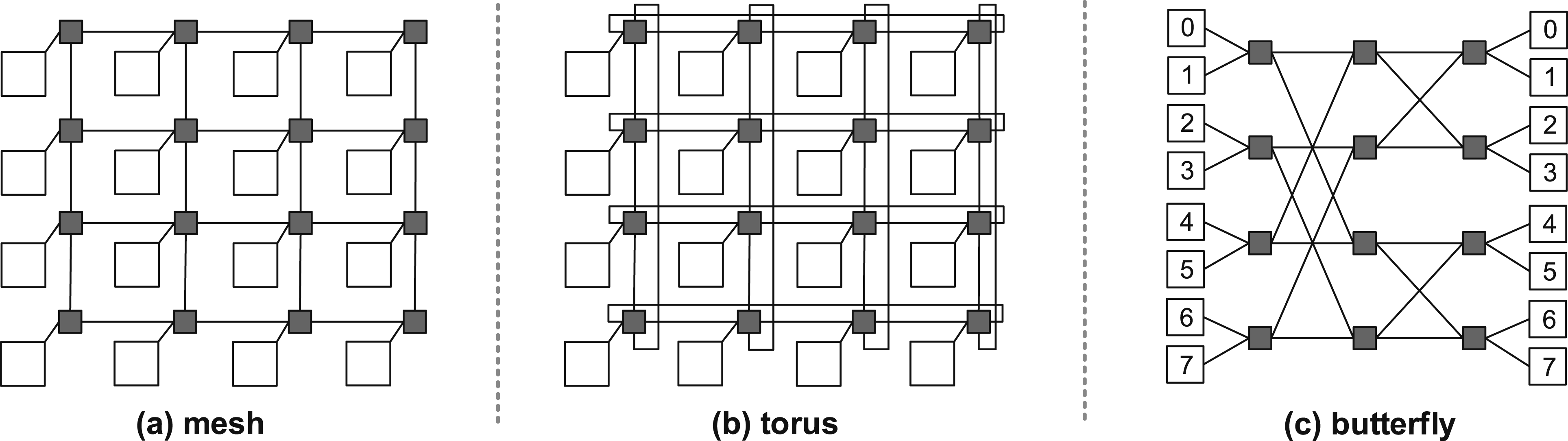
Network-on-chip (NoC) architectures
Despite offering simplicity and a low area overhead, bus-based architectures do not scale well as the number of cores and processing units on the chip keeps increasing, due to their inherent shared nature. To address this issue, modern devices with heterogeneous cores employ a Network-on-chip (NoC) architecture to overcome the scalability issues of bus-based architectures (Alimi et al., 2021; Amin et al., 2020; Benini and De Micheli, 2002; Kundu, 2014). NoCs use packets to route data from source to destination components by using a network fabric that consists of switches, routers and interconnect links. In bus-based architectures, very long wires are often used to connect distant components, which can lead to long wire delays. Instead, NoCs address the wire delay problem, by cutting down the communication links and inserting routers in between, in a more structured manner. All links can transfer data simultaneously and independently, allowing for much higher on-chip bandwidth.
There are several factors that define an NoC architecture, mainly the network topology, the switching strategies and the routing algorithms (Pasricha and Dutt, 2010). The network topology specifies how the components, the switches and the links are laid out and connected to each other. There are three main categories: (a) direct network topologies
106
, where each node in the network is directly connected to a subset of the other nodes; (b) indirect networks
107
, where nodes are only connected to switches and switches are directly connected to subsequent switches; and (c) irregular networks that can use a mixture of NoC and bus-based topologies. Figure 5 shows two examples of direct NoC topologies, namely the mesh and the torus, and one example of an indirect NoC topology, the butterfly. The switching strategies determine how the data (packets) flow through the routers in the network. Two main strategies exist, circuit-switching and packet-switching
108
. Finally, the routing algorithms define what paths are chosen in the network for the communication between a source and a destination. The efficiency of the routing algorithms is a critical factor in the NoC’s attainable performance as they directly affect network contention and, thus, the system-wide communication bandwidth.
109
As the network bandwidth reaches hundreds of Gb/s, more functionalities are being added to the network interface card, mainly to reduce the network and application overhead from host CPU.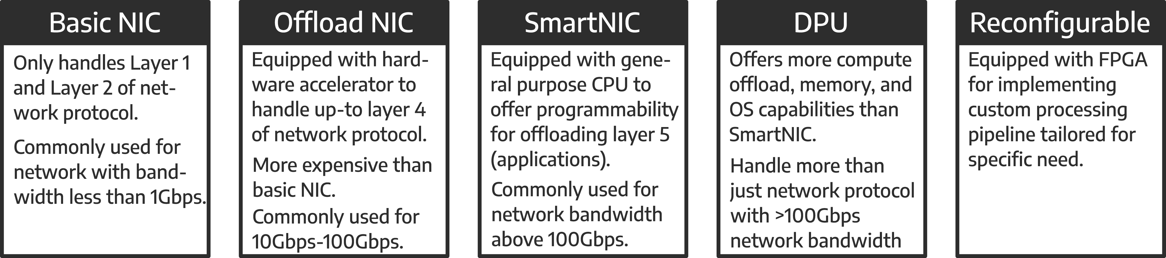
Software for on-chip communication
As SoCs are typically built around a microprocessor (CPU), on-chip communication is usually orchestrated by the CPU using device drivers, when in the presence of an operating system. Device drivers are responsible for mapping the memory space of each of the SoC components to the CPU’s memory space. Driver software is typically written in C/C++ or assembly code and is inherently complicated. Some works propose microarchitecture extensions that bypass driver complexity and overheads (Asri et al., 2020) or high-level software directives (Sommer et al., 2017; Tsog et al., 2021) that directly offload workloads to the accelerators by simply annotating a software code’s candidate region with special instructions and intrinsics. In any case, high-level tools with easy-to-use APIs are often provided by vendors to simplify the communication for the end-user, such as CUDA (Buck, 2007), ROCm (Sun et al., 2018) and Vitis. Thus, to initiate a transaction, the user simply needs to define its size and data type, as well as the source and the destination.
Intra-node communication
A compute node typically comprises a general-purpose microprocessor, its off-chip memory, and its peripherals. The peripherals may include hardware accelerators, network communication interface 110 , and non-volatile memory. The interface between the microprocessor and its off-chip memory has been reviewed in the DRAM section. In this part, we review the interface between the microprocessor and its peripherals.
Historical trends and key technologies
Evolution of intra-node device-to-device communication link.
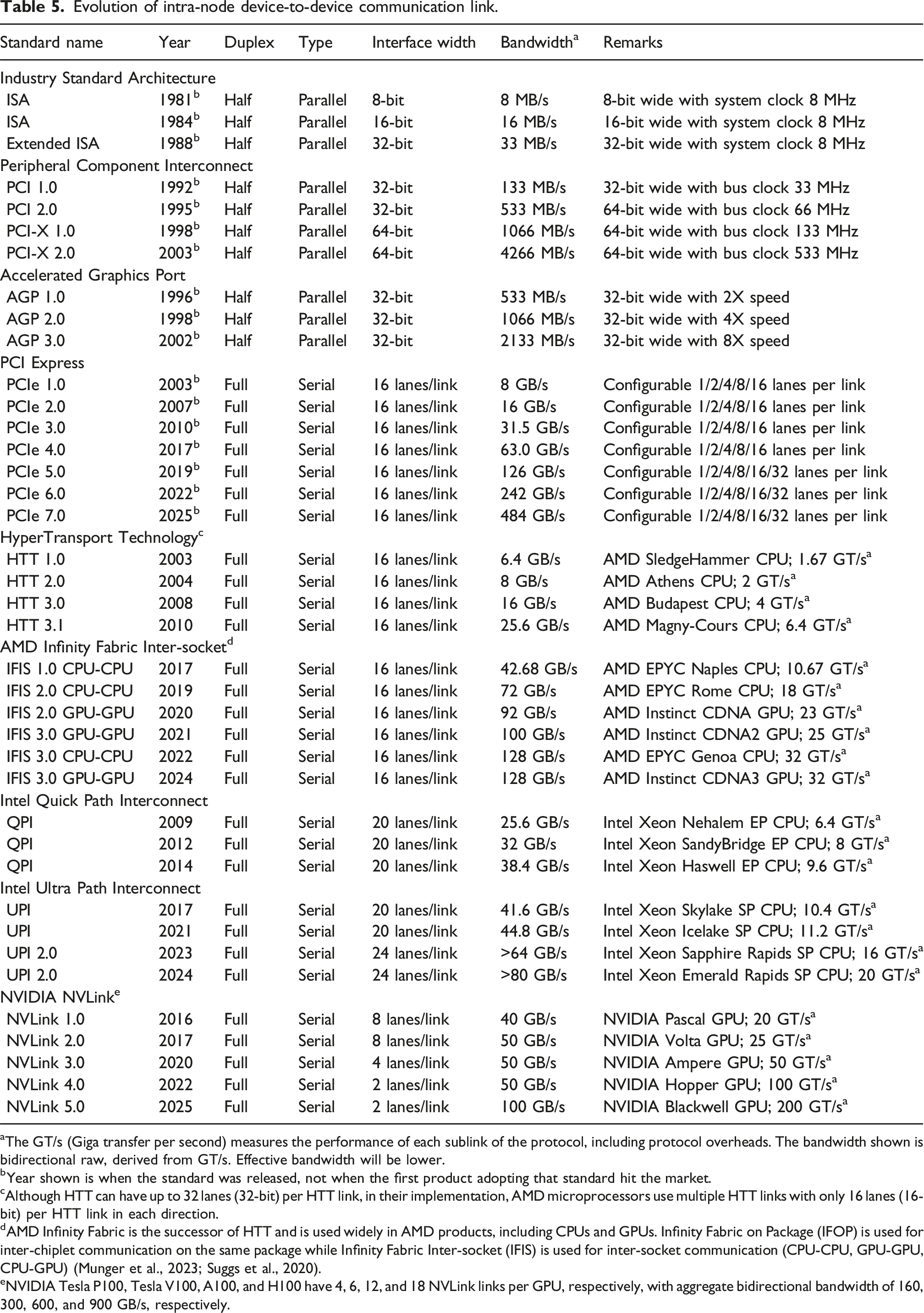
aThe GT/s (Giga transfer per second) measures the performance of each sublink of the protocol, including protocol overheads. The bandwidth shown is bidirectional raw, derived from GT/s. Effective bandwidth will be lower.
bYear shown is when the standard was released, not when the first product adopting that standard hit the market.
cAlthough HTT can have up to 32 lanes (32-bit) per HTT link, in their implementation, AMD microprocessors use multiple HTT links with only 16 lanes (16-bit) per HTT link in each direction.
dAMD Infinity Fabric is the successor of HTT and is used widely in AMD products, including CPUs and GPUs. Infinity Fabric on Package (IFOP) is used for inter-chiplet communication on the same package while Infinity Fabric Inter-socket (IFIS) is used for inter-socket communication (CPU-CPU, GPU-GPU, CPU-GPU) (Munger et al., 2023; Suggs et al., 2020).
eNVIDIA Tesla P100, Tesla V100, A100, and H100 have 4, 6, 12, and 18 NVLink links per GPU, respectively, with aggregate bidirectional bandwidth of 160, 300, 600, and 900 GB/s, respectively.
Data rate, and bus clock frequency
Copper-based wires are popular for very short-to medium-distance communication links due to their low manufacturing cost and high reliability. However, they already have met their technological limits (Part I: Wiring, connectivity, and signal integrity (Hanindhito et al., 2026)). Increasing the bus clock frequency, which is required to achieve higher bandwidth in synchronous serial interfaces 111 is challenging due to data integrity issues, especially over a long distance 112 (Kumar et al., 2023). Using other materials, such as platinum-group metals, or using optical signals (Part I: Optical interconnects (Hanindhito et al., 2026)), are among viable options for increasing the communication bandwidth.
Bus encoding and bus overhead
Modulation and encoding are needed before data is transmitted (Part I: Signal coding and modulation (Hanindhito et al., 2026)). Although denser modulation shapes promise higher bandwidth, they have higher bit error rates 113 , and necessitate using a more advanced error correction mechanism 114 . Accordingly, a more advanced physical layer implementation (SerDes) to support a more advanced error correction mechanism (Aziz et al., 2011; De Paulis et al., 2022; Drenski and Rasmussen, 2018; Yue and Shekhar, 2022), and a more efficient (block) coding is needed to enable higher data rates. This adds more transistors to the microprocessor, and increases power consumption (Part I: Architecture of communication interfaces (Hanindhito et al., 2026)).
Bus width and routing complexity
Adding more serial lanes increases the communication bandwidth; however, this is expensive 115 (Part I: Architecture of communication interfaces (Hanindhito et al., 2026)). Many modern serial interfaces 116 utilize multiple serial lanes, where some of them permit a flexible configuration 117 for the number of lanes, based on bandwidth requirements.
Data transfer energy consumption
Longer-distance data transmission entails more energy consumption 118 (Keckler et al., 2011; Kestor et al., 2013). High-frequency signals consume more power, due to the effect of parasitic capacitance at higher frequencies (Tran, 2023). Lastly, a more advanced physical layer implementation (SerDes) consumes more power, which must be accounted for in the total power budget of the chip (Abdennadher et al., 2020; Rashdan et al., 2009, 2020).
Standardization and industry adoption
Communication interfaces are used to connect various devices. Their adoption by multiple hardware vendors enables compatibility and interoperability among different devices when each device is provided by a different vendor. The Common Electrical I/O (CEI) (Part I: Architecture of communication interfaces (Hanindhito et al., 2026)) is an effort to achieve standardization. Accordingly, multi-standard, multi-mode physical interfaces (SerDes) have been developed, which can then be used to implement various communication protocols (Chattopadhyay et al., 2018; Lin et al., 2021; Nishi et al., 2008; Roshan-Zamir et al., 2017; Vamvakos et al., 2012), reducing the development cost and time. An example of a widely adopted interface is PCI Express. On the other hand, proprietary interfaces, such as NVIDIA NVLink (Wei et al., 2023), and AMD InfinityFabric, are limited to devices that are provided by their respective vendors. The use of proprietary interfaces allows manufacturers to optimize their implementation to achieve more efficient interoperability across different devices from the same vendor. However, future computing systems will move toward more open and standardized interfaces, such as Open Compute Project (OCP) (Frachtenberg, 2012), Compute Express Link (CXL) (Sharma, 2022c; 2023a), and Universal Chiplet Interconnect Express (UCIe) (Das Sharma et al., 2022).
Connection topology
Due to the availability of various communication interfaces, a computer system often uses different types of interfaces, along with different connection topologies (Kong et al., 2023). For instance, a GPU-accelerated compute node may use AMD Infinity Fabric (interface) for inter-socket CPU communication, PCI Express (interface) for CPU-to-GPU, and CPU-to-NVMe 119 communication, and NVIDIA NVLink (interface) for GPU-to-GPU communication. Applications and communication libraries must be able to identify each communication interface, along with the connection topology between them (Amaral et al., 2017; Chu et al., 2020; Li et al., 2020; Muthukrishnan et al., 2021). This enables them to choose the most efficient interface for exchanging data between different devices.
Coherency
PCI Express has been widely used as a communication interface between microprocessors and various devices (Mayhew and Krishnan, 2003). However, PCI Express does not have built-in support for maintaining cache and memory coherency (Lutz et al., 2020; Stuecheli et al., 2015). Therefore, the coherency must be handled at the software level 120 . With the proliferation of hardware accelerators (Part I: Hardware accelerators (Hanindhito et al., 2026)) and heterogeneous computing, efficient communication interfaces and protocols become more important, especially for resource sharing and memory management.
Compute express link (CXL)
The Compute Express Link (CXL) is an open standard protocol, which provides a cache- and memory-coherent communication interface between microprocessors, memory, and hardware accelerators (Sharma, 2022c; 2023a). It uses PCI Express as its physical layer, with added coherency protocol between microprocessors and the attached devices, which allows simplified resource sharing (Cabrera et al., 2022; Jung, 2022). Therefore, it can limit the involvement of users in managing the memory of hardware accelerators. CXL aims to improve communication performance across multiple devices, simplify the software stack, and lower the overall system cost.
The first generation of CXL, CXL 1.0/1.1 (2019), introduced three types of protocols: (a) CXL.io, which has the same functionality as the PCIe protocol; (b) CXL.cache, which allows hardware accelerators to efficiently access host microprocessor’s memory; and (c) CLX.mem, which permits host microprocessors to access device-attached memory. These protocols enable the coherent sharing of memory resources between the host microprocessor and different devices 121 . The second and third generation of CXL (2020, 2022, respectively) primarily deal with inter-node communication.
Software for intra-node communication
Communication between different devices on a node, e.g. CPU-CPU, CPU-GPU, GPU-GPU etc. can be realized using interfaces, such as PCIe, Ultra Path, NVLink. In software, intra-node communication between CPUs was historically first managed by using pthread, a low-level, shared memory execution model compliant with most operating systems. To improve productivity, libraries like OpenMP were developed that offer easy-to-use, high-level APIs. By contrast, inter-node communication was handled using Message Passing Interface (MPI) libraries, such as OpenMPI (Gabriel et al., 2004) and MVAPICH (Panda et al., 2021). As modern nodes comprising both CPUs and GPUs grew in popularity, MPI libraries began to be utilized for intra-node communication as well, due to extensions that allowed CPU-GPU communication. Some of these libraries are also GPU-aware 122 , allowing efficient CPU-GPU and GPU-GPU communication. These libraries enable direct GPU-GPU communication, without the requirement of staging data through the host CPU memory.
Off-chip accelerator devices, such as FPGAs and ASICs are typically connected to a host CPU device via a PCIe IO interface (Firoozshahian et al., 2023; Jouppi et al., 2017, 2023; Prabhakar et al., 2022). Similarly to on-chip communication, the CPU can orchestrate transactions with the FPGA or the ASIC by using device drivers. Again, the use of high-level APIs can greatly boost productivity for the end user. Direct off-chip communication between FPGAs or ASICs requires implementation of low-level hardware mechanisms, which are more complicated in nature. A sophisticated software stack support is required to abstract this complexity from the end user.
Inter-node communication
Only a limited amount of processing power, memory, and storage, can be placed on a single compute node 123 . Power delivery and thermal dissipation are among the main limiting factors 124 . Moreover, the pin scarcity of CPUs limits the number of memory channels and off-chip interconnection links, which, in turn, limits how much memory, storage, and accelerator cards a single compute node can have. To be able to handle increasingly larger problem sizes, multiple compute nodes are typically utilized. The interconnection between compute nodes is the weakest link in the inter-device communication. Inter-node communication often limits the overall performance (Rumley et al., 2020), and consumes considerable amounts of energy (Georgakoudis et al., 2019), especially for workloads that have excessive inter-node data movement.
Technologies and standards
HPC inter-node interconnection technology landscape.
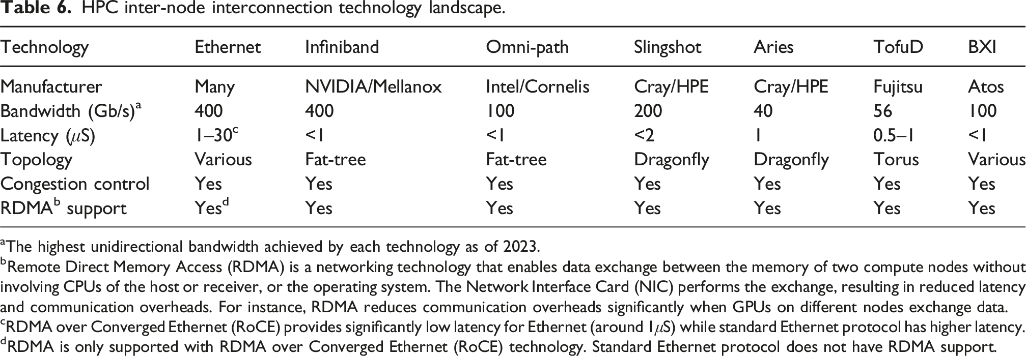
aThe highest unidirectional bandwidth achieved by each technology as of 2023.
bRemote Direct Memory Access (RDMA) is a networking technology that enables data exchange between the memory of two compute nodes without involving CPUs of the host or receiver, or the operating system. The Network Interface Card (NIC) performs the exchange, resulting in reduced latency and communication overheads. For instance, RDMA reduces communication overheads significantly when GPUs on different nodes exchange data.
cRDMA over Converged Ethernet (RoCE) provides significantly low latency for Ethernet (around 1μS) while standard Ethernet protocol has higher latency.
dRDMA is only supported with RDMA over Converged Ethernet (RoCE) technology. Standard Ethernet protocol does not have RDMA support.
Ethernet interconnects have been popular in large-scale clusters due to their lower cost, e.g. multi-gigabit Ethernet interconnects, with 100 Gb/s bandwidth and beyond. In June 2023, 45.4% of clusters in the Top500 list used Ethernet as their inter-node communication, with 37.8% of them supporting 100 Gb/s. None of the clusters in the Top50 list use multi-gigabit Ethernet, as most 125 of them use InfiniBand.
InfiniBand has been adopted by 40% of the clusters in the Top500 list, with 32.5% of them supporting 200 Gb/s High Data Rate (HDR), and 30% of them supporting 100 Gb/s Extended Data Rate (EDR) and HDR combined. Other clusters in the Top500 list use 100 Gb/s Slingshot-10 (3.4%), 200 Gb/s Slingshot-11 (3%), and 100 Gb/s Omnipath (7%).
InfiniBand history and future roadmap.
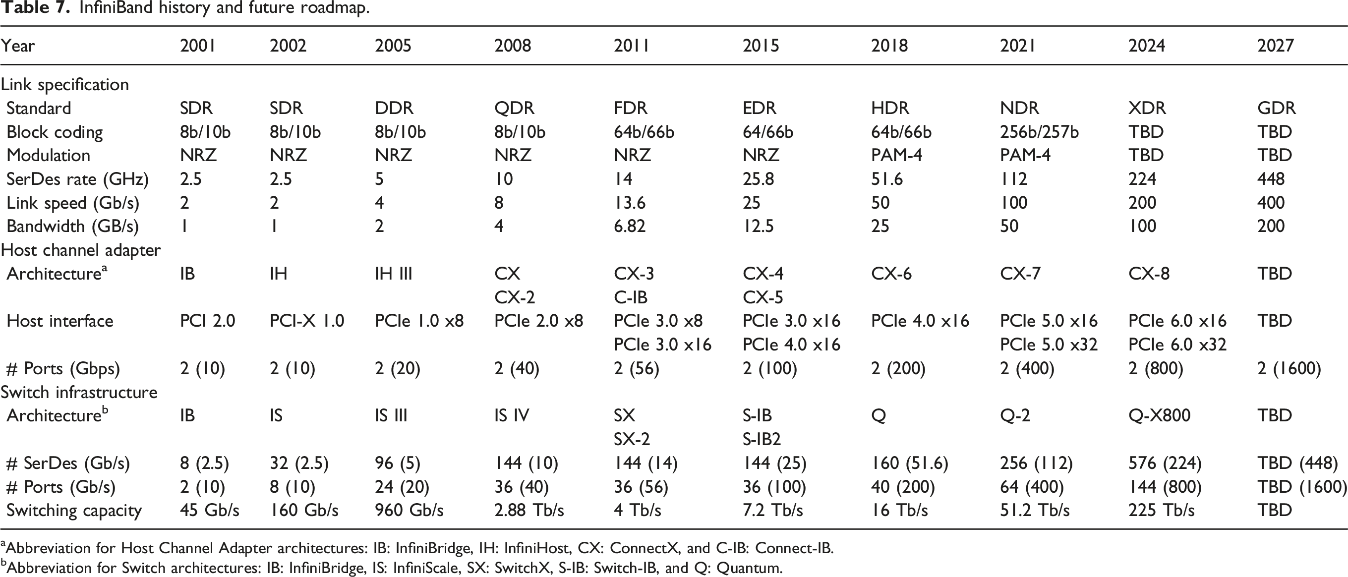
aAbbreviation for Host Channel Adapter architectures: IB: InfiniBridge, IH: InfiniHost, CX: ConnectX, and C-IB: Connect-IB.
bAbbreviation for Switch architectures: IB: InfiniBridge, IS: InfiniScale, SX: SwitchX, S-IB: Switch-IB, and Q: Quantum.
SDR
InfiniBand emerged in 1999 as InfiniBand Trade Association (IBTA), from the merger of two competing technologies: Future I/O, and Next Generation I/O (NGIO). Mellanox, which was founded in 1999 to develop NGIO, shipped its first InfiniBand product, InfiniBridge, in 2002. InfiniBridge is an integrated host channel adapter 127 (HCA) and switch 128 , capable of providing eight 1X InfiniBand lanes at 2.5 Gb/s; or two ports, each having 4X InfiniBand lanes, enabling a total bandwidth of 10 Gb/s, known as Single Data Rate (SDR) (Deirling, 2001; Eddington, 2002).
Either copper or optical cables 129 can be used to connect two InfiniBand points (e.g., HCA to a switch). The PCI interface (Table 5) turned out to be the limiting factor on how much bandwidth the HCA can achieve. Therefore, in 2003, Mellanox introduced InfiniHost with PCI-X interface for the HCA chip, along with a dedicated switching chip, called InfiniScale. InfiniScale had eight 4X InfiniBand ports, with improved scalability and switching capacity for larger clusters.
DDR
As serial clock rates advanced to 5 GHz, the Double Data Rate (DDR) version of InfiniBand was introduced in 2005, with InfiniHost III HCA chip, and InfiniScale III switching chip.
The InfiniHost III HCA was the first InfiniBand HCA to use PCI Express interface to provide more bandwidth between host CPU and HCA. The InfiniScale III was the first switching chip to reach almost 1 Tb/s of switching capacity. DDR had twenty-four 4X InfiniBand ports, and enabled a total bandwidth of 20 Gb/s.
QDR
In 2008, Mellanox released its fourth-generation HCA, named ConnectX (Sur et al., 2007), which provided significantly lower latency, higher packet processing 130 performance, and higher bandwidth; it was first used in Quad Data Rate (QDR) InfiniBand. It features the Virtual Protocol Interconnect (VPI), which allows the HCA to be configured as either an Ethernet, or an InfiniBand card (Grant et al., 2009). This flexibility makes it easier for clusters to progressively adopt InfiniBand technologies, while keeping some of their less-demanding infrastructure 131 on Ethernet.
FDR
The VPI feature was also integrated into the switching chip, and was called SwitchX (2011). SwitchX uses a 14 GHz serial clock rate, and the new and more efficient 64b/66b block coding technique 132 (Part I: Signal coding and modulation (Hanindhito et al., 2026)), resulting in 4 Tb/s of switching capacity; along with ConnectX-3 HCA chip, it constitutes the Fourteen Data Rate (FDR) InfiniBand.
EDR
In 2015, Mellanox separated the switching chips: Switch-IB for 100 Gb/s Extended Data Rate (EDR) InfiniBand; and Spectrum for 100 Gb/s Ethernet 133 . Nevertheless, the ConnectX HCAs was still used to support both InfiniBand and Ethernet, using VPI.
HDR
The High Data Rate (HDR) InfiniBand switched from NRZ modulation to PAM-4 modulation, in order to push more data into the cables. HDR achieved 200 Gb/s bandwidth on 4X InfiniBand links, with a 51.6 GHz serial clock rate. The Quantum switching (2018) chip provides 16 Tb/s of switching capacity, with forty 200 Gb/s InfiniBand ports.
NDR
The Next Data Rate (NDR) was released in 2022, with a 112 GHz serial clock utilizing PAM-4 modulation and 256b/257b block coding.
XDR
The Extreme Data Rate (XDR) was released in 2024 with 224 GHz SerDes (Chan et al., 2022).
Going forward, adoption of inter-node communication technologies will depend on how a cluster is intended to be utilized. Multi-gigabit (e.g., 50 Gb/s to 200 Gb/s) Ethernet will likely see rapid deployment on mainstream enterprise clusters 134 , as they are cost-effective, and easy to implement. HPC clusters will likely use 100 Gb/s to 200 Gb/s Ethernet, InfiniBand, or their equivalent technologies for CPU-based clusters, and 400 Gb/s InfiniBand or their equivalent technologies for GPU-based clusters. Cloud clusters will likely aim for 100 Gb/s to 400 Gb/s interconnection technologies, based on their workloads 135 . Bandwidth-hungry AI- or ML-clusters will likely need an even higher bandwidth, possibly in the range of 800 Gb/s or beyond; this will make them early adopters of advanced interconnection technologies.
Network interface card (NIC) and data processing unit (DPU)
The basic functionality of a network interface card (NIC) is to allow each node to communicate with other nodes through a particular networking standard 136 . Basic NICs can only perform lower-level network protocol functions, while the CPU handles the higher-level protocols. Offload NIC is a hardware accelerator that performs higher-level network protocol functions 137 (Maccabe et al., 2002; Shivam and Chase, 2003), and thus, removes the burden from the host CPU. The offloading strategy becomes more important for higher bandwidth networks (e.g., 1 Gb/s and 10 Gb/s Ethernet), since the network protocol overheads become larger, and can consume significant cycles from the host CPU. However, this offloading mechanism is often limited to the TCP/IP layer or below 138 (Pismenny et al., 2021a). Therefore, the host CPU must still handle the application layer and above 139 , such as data encryption and decryption (Pismenny et al., 2021b; Sabin and Rashti, 2015), data compression and decompression (Li et al., 2023), storage protocols (Kim et al., 2021a; Zhang et al., 2023), remote procedure call protocols, and key-value store protocols.
With network bandwidth at or exceeding hundreds of Gb/s, the overhead of network applications becomes more significant. SmartNICs extend the capabilities of Offload NICs, by integrating a general-purpose CPU into the NIC (Figure 6). This offers programmable offloading capabilities for network applications 140 (Qiu et al., 2020). Data processing units (DPUs) extend SmartNICs, by providing even more compute capabilities and memory capacity. Accordingly, DPUs enable running more complex data-intensive applications in NIC, such as using neural networks to detect security threats on traffic flows throughout the computing infrastructure (Tasdemir et al., 2023), data encryption, and traffic management and scheduling 141 . To enable the development of custom computing pipelines that are tailored for specific needs, a reconfigurable DPU could be used, which is a DPU with an integrated FPGA (Caulfield et al., 2018; Dastidar, 2023; Trivedi and Brunella, 2023).
We remark that a robust and easy-to-use software stack is also important for the end users to optimally harness the performance and efficiency that is offered by DPUs. We highlight a few DPU products next:
NVIDIA BlueField-2 DPU
It combines ConnectX-6 with 8-core ARM A72 CPUs, to offload critical networking, storage, and security tasks from the host CPUs. BlueField-2X DPU adds a GPU 142 into the same PCB that hosts the ConnectX-6 NIC and the ARM CPU, in order to run AI or ML analytics tasks on the data while the data is being transmitted. This capability, for instance, could benefit the telecommunication industry.
BlueField-3 DPU
It improved its predecessor by combining ConnectX-7 with 16-core ARM A78 CPUs, in order to improve its throughput and processing power.
Other products
Other vendors followed the same approach by introducing their own DPUs, such as AMD, with their Pensando DPU, and Intel, with their Infrastructure Processing Unit (IPU).
Network topologies
While the bandwidth of inter-node communication is increasing, connecting all nodes within a large cluster is challenging. Even with the most advanced switches, with Terabytes per second of switching capacity, there will not be enough ports to directly connect all nodes (Maniotis et al., 2020, 2022; Teh et al., 2022; Villar et al., 2013; Yan et al., 2021). Instead, multiple switches are used to provide connection between different parts of a cluster (Alizadeh and Edsall, 2013; Krause et al., 2018; Li et al., 2015b): leaf switches, to provide connection between nodes within the same rack; spine switches, to provide connection between racks; and sometimes super-spine switches, to provide connection between spine switches in extremely large clusters.
Each cluster may have a different inter-node interconnection topology, with different characteristics in terms of bandwidth and latency between nodes.
For instance, the Frontera cluster (2019) at the Texas Advanced Computing Center (TACC) uses two-level switches in a fat-tree topology. AI or ML clusters may use a more complex topology, with multi-rail InfiniBand per node 143 . Optimizing software and workloads when running on a specific cluster (e.g., by partitioning a workload appropriately across different nodes) may significantly impact the overall performance.
Disaggregated infrastructure
Data centers or HPC clusters have three main components in their compute racks (infrastructure): compute, storage, and network. The compute part is provided by a large number of servers interconnected to each other. The network part is responsible for providing high-bandwidth and low-latency connections to the servers, allowing them to work together. Each server may have a different configuration, essentially resembling a stand-alone computer, where they have their own processors, memory (e.g., DRAM), peripherals (e.g., GPUs), and storage. However, using local storage creates challenges for managing data across different servers. Accordingly, centralized storage is typically provisioned to provide parallel, scalable data access across all servers. This choice also eases replicating the storage for backup. Figure 7 illustrates different types of infrastructure for data centers and HPC clusters (Park et al., 2022). Examples of infrastructure (compute rack) in data centers and HPC clusters (Haag, 2018): (a) traditional, with separate compute, network, and storage entities (left); (b) converged, with pre-validated, packaged components (middle); and (c) disaggregated, with pooled resources (right). For comparison, an image of a representative cluster showing three compute racks is also included.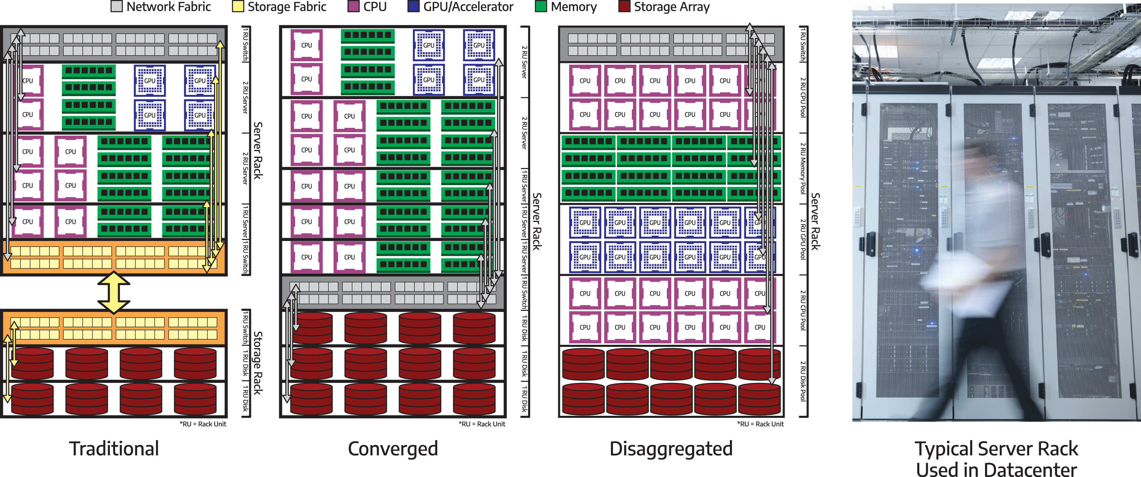
Traditional infrastructure implements the three components as separate entities, often from different manufacturers. In this manner, servers that implement the compute are connected through a networking fabric 144 . On the other hand, storage is usually implemented by using proprietary hardware, which often comes with its own proprietary networking fabric 145 . These four components must be architected to work together as a cluster system. Deploying and maintaining these components, possibly from different manufacturers, is costly and inefficient (Haag, 2018).
Converged infrastructure is a pre-packaged and pre-validated compute, storage, and network, which is provided by a single manufacturer. While individual components can be manufactured by different vendors, they have been validated to work together (Garber, 2012). This guarantees their interoperability and reliability, enabling seamless integration and scalability. In this design approach, the storage system is commonly implemented with commodity hardware and typically shares the same network fabric for communication that the rest of the components are using. This eliminates the need for using a specialized storage fabric, and greatly simplifies deployment and maintenance of the infrastructure. However, it adds pressure to the network as it needs to handle both the compute and storage traffic.
The composable/disaggregated infrastructure (CDI) provides pooled resources 146 in physically separated units or racks that can be allocated dynamically based on specific needs of an application. Consequently, each server is no longer a complete compute system. In the extreme case, there may be entire racks with pooled CPUs versus pooled memory versus pooled discs. Accordingly, CDI allows resource allocation at finer granularity, which improves efficiency. However, interconnection between devices can be challenging, and requires further advancements in communication technologies 147 , including silicon photonics (Michelogiannakis et al., 2023).
While CXL 1.0/1.1 focuses on interconnects on a single node (Sharma, 2019), subsequent versions of CXL, i.e. CXL 2.0 (Sharma, 2020a) and CXL 3.0 (Sharma, 2022b), focus on cluster-wide resource sharing 148 . These technologies make the implementation of future CDIs easier. With copper wires approaching their end of life when it comes to support low latency, high bandwidth, and long-distance communication, optical and silicon photonics will become key drivers in the future of cluster computing with CDI.
Shared infrastructure
Computing infrastructure is built differentially for HPC, AI/ML, and cloud computing, due to their unique requirements. For instance, advanced AI/ML applications typically run communication-intensive workloads. They exploit the latest hardware accelerators (e.g., GPUs), the most advanced network technologies, and interconnect topologies that are available today. HPC applications demand significant compute power. They use high-bandwidth, low-latency interconnects, although not always as demanding as AI/ML applications. On the other hand, cloud computing has low or moderate requirements, depending on (micro)-services they serve. Accordingly, AI/ML, HPC, and cloud infrastructure have been evolving independently for decades. Nevertheless, since the demand for computing is rapidly increasing, and the cost of building computing infrastructure is surging, designing infrastructure that supports a more diverse workload is becoming more desirable. For instance, by adopting the Everything-as-a-Service 149 model of cloud computing, Acceleration-as-a-Service (XaaS) (Hoefler et al., 2024) enables running HPC applications in a computing infrastructure that adopts cloud-computing principles (i.e., containerization). Accordingly, resources are allocated based on container types (e.g., HPC container, or cloud service container), ensuring better utilization and lowering the total cost of ownership for such computing infrastructure.
What comes next?
At the on-chip and in-package level, with trends of breaking large monolithic chips into smaller chiplets (Part I: Advanced packaging technologies (Hanindhito et al., 2026)) that are integrated in one package, communication between chiplets may limit the overall performance of chips for some applications (Chirkov and Wentzlaff, 2023). The Universal Chiplet Interconnect Express (UCIe) provides a milestone for open industry standards for future chips that use the chiplet packaging technology (Das Sharma et al., 2022; Sharma, 2023b).
Development of intra-node interconnects will continue according to the trend shown in Table 4, and will depend heavily on advances in SerDes (Part I: Architecture of communication interfaces (Hanindhito et al., 2026)) and silicon photonics technologies (Michelogiannakis et al., 2023), given that electrical signals on metal wires have hit their bandwidth limits. A key desire is development of intra-node interconnects that are as fast as the interconnect between chips and off-chip memory. This can especially be beneficial to workloads that deal with vast amounts of data, which require aggregate memory capacity across multiple devices.
Finally, inter-node interconnects will rely heavily on optical communication, which is a key enabler of disaggregated infrastructure. Similarly to intra-node interconnects, providing inter-node bandwidth that is on par with off-chip memory bandwidth is a key objective. Processing-in-network 150 will become more popular in communication-intensive workloads since it offloads data aggregation computations 151 to modern network switches and SmartNICs, which minimizes the amount of data that is needed for communication and thus lowers overhead for CPUs and GPUs.
System integration and heterogeneous computing
In order to keep up with modern computational and power requirements, systems comprising CPUs, GPUs and/or other accelerators are typically employed. In this section, we discuss challenges associated with deciding what type of system a given application should be run on and how its different components should be integrated.
While GPUs and other hardware accelerators offer much higher performance and energy efficiency for a certain class of applications, they are not meant to replace general-purpose microprocessors (CPUs). The CPUs are still needed for running operating systems and drivers (Chishiro et al., 2019; Stuecheli et al., 2015), orchestrating resources (e.g., memory, data) between devices (Bolchini et al., 2015; Hamano et al., 2009; Panneerselvam and Swift, 2016; Usui et al., 2016; Yogatama et al., 2022), and executing non-accelerated workloads 152 (Agosta et al., 2018; Baskaran et al., 2022; Marongiu et al., 2015; Tsog et al., 2021). The use of multiple such types of processing units in a well-orchestrated and coordinated way to provide improvements in performance and energy efficiency is called heterogeneous computing (Khokhar et al., 1993; Zahran, 2017), which is an ongoing trend that is expected to continue (Shafique and Garg, 2017).
To this end, two types of heterogeneous systems exist. First, systems that comprise multiple different devices on the same node, such as a CPU, a GPU and/or an FPGA or ASIC. Each of these chips can be a completely different hardware platform and have its own dedicated memory (e.g. DRAM or HBM). Intra-node communication between these chips is realized via dedicated links, such as PCIe, NVLink, Ultra Path Interconnect, or newer CXL-based technologies. Second, the individual chips themselves may be heterogeneous (SoCs), in that they can encapsulate multiple types of processing units on the same package, where each processing unit may be part of a different in-package chiplet. One simpler example of such systems is heterogeneous CPU devices, such as the ARM big.LITTLE and Intel Alder Lake (Rotem et al., 2022) architectures, which contain high-power, high-performance with low-power, high-efficiency cores, a method which reduces power during execution of relatively lighter workloads. These cores may exhibit heterogeneity in their microarchitecture, but all use the same instruction set architecture. On the other hand, popular examples of more complex SoCs comprising entirely different processing units include: (a) Apple M1–M4 (Ali et al., 2022; Kasperek et al., 2023; Kenyon and Capano, 2022; Zhang, 2021), used in Mac laptops and iPad tablets, which integrate CPU, GPU, and Neural Processing Unit (NPU) cores on a single chip, with the NPU specifically dedicated to accelerating AI workloads. Similarly, Apple’s A16–A18 chips also comprise CPU, GPU and NPU cores, but are instead targeted for smartphones (iPhone); (b) the NVIDIA Grace-Hopper (Evans, 2022; Wei et al., 2023) and Grace-Blackwell (Tirumala and Wong, 2024) super chips and AMD Mi300a (Patel et al., 2023), that integrates CPU and GPU chiplets; and (c) AMD/Xilinx’s Versal Adaptive Compute Acceleration Platform (ACAP) (Ahmad et al., 2019) that comprises a CPU, an FPGA, and an AI Engine (AIE) array consisting of up to 400 programmable VLIW/SIMD processors. SoCs are becoming increasingly popular, as integrating accelerators on the same chip can greatly reduce communication costs that relate to performance and power. However, naively moving the accelerator on-chip may not always be advantageous compared to using off-chip accelerators. Additional optimizations are often required to properly manage all the resources and extract maximum performance (Asri et al., 2021). In the following, we discuss on-chip, intra- and inter-node integration aspects of heterogeneous systems. We end by describing Anton, which is a heterogeneous computing system customized for molecular dynamics simulations.
On-chip integration
Heterogeneous SoCs with a diversity of compute platforms and connectivity mechanisms can be complicated and usually require systematic methods for efficient utilization. Key issues related to these devices are the data-sharing between the processing units and how tasks should be partitioned and scheduled across them.
In terms of data-sharing, there are three approaches (Cota et al., 2015; Giri et al., 2018; Peccerillo et al., 2022): (a) non-coherent accelerators, in which each accelerator and the CPU have separate memory spaces, where the data-sharing can be achieved using direct memory access (DMA) (Kim et al., 2021d; Ma et al., 2019; Pham-Quoc et al., 2013; Su et al., 2011; Wang et al., 2021a). DMA is managed by users or the software libraries (Awamoto et al., 2020; Gong et al., 2014); (b) accelerators with coherency at the last-level cache, in which the accelerators share the data with the last level cache of the CPU (Asri and Gerstlauer, 2022; Garcıa et al., 2016; Mekkat et al., 2013); and (c) fully-coherent accelerators, in which a cache coherency protocol handles the data coherency between the CPU and the accelerators, (Kumar et al., 2015; Olson et al., 2017), thus simplifying programming (Lim and Kim, 2012). Some recently released heterogeneous architectures use full-coherence unified memory to simplify programming. Examples include Apple M1 and M2 SoCs (Ali et al., 2022; Kasperek et al., 2023; Kenyon and Capano, 2022; Zhang, 2021), NVIDIA Grace-Hopper super chip (Evans, 2022; Wei et al., 2023), and AMD Mi300a (Patel et al., 2023).
The software stack 153 can boost productivity by detecting available accelerators and offloading tasks to them, hiding most of the inherent complexity from the programmers (Andrade and Crnkovic, 2018; Bragança et al., 2018; Castrillon et al., 2018; Gummaraju et al., 2010; Wang et al., 2018; Zhong et al., 2019; Zuckerman et al., 2021). While the robustness of the software stack 154 can influence the adoption rate of the accelerators in a heterogeneous device, it is not enough for efficiently utilizing all available resources of these devices. One major question that first needs to be answered is what runs where and when. Each computing platform is suitable for different types of workloads. For example, tasks with canonical, mature and widely-used kernels with a large degree of parallelism and a high arithmetic intensity 155 may best be suited for ASICs. Highly memory-bound 156 tasks with inherent parallelism may best be suited for GPUs, due to their large memory bandwidth. Tasks with complicated control flows and limited parallelism are best executed on CPUs. Additionally, the communication cost between different resources in a system is a crucial factor in attainable performance that can affect where each task should be mapped to. Ultimately, maximizing an application’s performance on a heterogeneous system is a hardware/software partition and scheduling problem.
The partition problem refers to the assignment of an application’s tasks to processing units that optimizes metrics, such as execution time and energy consumption. The scheduling problem refers to mapping each processing unit’s tasks to a start time, such that performance is maximized. These problems become increasingly difficult with the complexity of modern heterogeneous platforms. Different strategies that use exact 157 , constructive 158 , or iterative 159 methods can be used in practise to find optimal or sub-optimal solutions. As each vendor’s SoCs use widely different architectures and means of communication, no universal tools that automatically solve the hardware/software partition problem on all SoC platforms are available. However, SoCs typically come with a software suite that provides tools to help with the exploration and the integration of the system, such as CUDA (Buck, 2007), ROCm (Sun et al., 2018), and Vitis V++ compiler.
Intra-node integration
Nowadays, most devices in a node have their own on-chip memory and are separated from the host CPU. The host CPU is responsible for offloading a task to the accelerator device and reading the results back upon completion. Systems with newer CXL-based memory hierarchy will add more diversity. For example, multiple devices (e.g., CPUs, GPUs, ASICs) may use a unified address space, by sharing a single, large memory device on the compute node in a fully coherent manner, enabling high-bandwidth communication.
In all these cases, the same partitioning and scheduling problem mentioned earlier is applied for such heterogeneous systems. The main difference is that communication, which now accounts for off-chip data transfers, can typically be much slower compared to on-chip. Several tools and libraries are available that can efficiently solve the partition and scheduling problem of intra-node systems with minimal intervention from the programmer (Augonnet et al., 2009; Trott et al., 2022). Each tool supports different sets of architectures and application domains.
Inter-node integration
Inter-node communication can be very slow. However, it is necessary for workloads with very large datasets that require more memory and compute resources. Achieving high performance on these workloads requires identifying suitable types of nodes in a cluster, while also utilizing algorithmic optimizations that minimize inter-node data transfers.
With the advent of disaggregated infrastructure technologies, such as CXL 2.0 and 3.0, more flexibility is added for inter-node communication, which can enable implementations tailored to a workload’s needs. Resources, such as accelerators, memory, and storage, can be provisioned dynamically to each compute node 160 . For instance, instead of a rack full of identical compute nodes (which is common today), the disaggregated architectures will have a rack with some nodes containing only memory, some nodes only containing accelerators, and some nodes only containing CPUs. Then, available resources can be dynamically assigned per use case basis. For example, a workload may require two memory nodes and one accelerator node, whereas another workload may need a single memory node and four accelerator nodes. This way, memory, accelerators, and CPUs will no longer reside on the same PCB, as they will be located on different nodes, or even on different racks. This makes interconnection between nodes and racks crucial, in order to achieve the same or even better latency and bandwidth, compared to today’s architectures.
An example: Anton specialized chip and system for molecular dynamics
In this part, we consider an example of a heterogeneous and specialized computing system. Anton is an accelerator ASIC and system, developed by D. E. Shaw Research, to accelerate all-atoms molecular dynamics (MD) simulations (Deneroff et al., 2008; Dror et al., 2011). These simulations can predict three-dimensional movement of atoms based on their inter-atomic force interactions. The primary motivation for designing Anton seems to be the enablement of fast MD simulations for drug discovery. To the best of our knowledge, Anton is the only ASIC and ASIC-based system that has been developed primarily for advanced scientific computing. Anton (as a system) is not just a specialized chip: the specialized chip is complemented with the rest of the supercomputing ecosystem 161 , which has been specialized to run certain MD simulations as fast as possible. In this sense, the Anton supercomputer is truly unique, and therefore, we review it in more detail.
The first generation of the ASIC (Anton 1), launched in 2008, was manufactured using 90 nm process node technology, and had 200 million transistors that ran at 400 MHz of clock frequency (Shaw et al., 2021). The ASIC had four subsystems: a high-throughput interaction subsystem (HTIS), a flexible subsystem, a communication subsystem, and a memory subsystem.
HTIS handles the most compute-intensive parts of the targeted MD simulations, which are evaluation of the electrostatic and van der Waals interactions between a pair of atoms. Theory that is used for these calculations is well-established, and is unlikely to change during the lifetime of the ASIC. HTIS runs at twice the rate of the system clock, and features 32 pairwise point interaction modules 162 (PPIM). Since they handle the most compute-intensive components of the targeted MD simulations, and the algorithm to calculate them is not expected to change, PPIMs are the most hardwired components of the ASIC. The streaming architecture of each PPIM consists of a 26-stage pipeline, 18 fixed-point adders, 27 fixed-point multipliers, and three look-up tables. Despite being hardwired, multiplexers are included to provide some degree of configurability. HTIS is controlled by a programmable general-purpose processor, referred to as the interaction control block (ICB) core.
The flexible subsystem controls the operation of the ASIC, computes the bond forces, performs FFT and inverse FFT, carries out time integration, and controls the simulation time-step. The flexible subsystem has four processing slices. Each slice comprises a single-core general-purpose (GP) CPU (Tensilica), a remote access unit (RAU), and two geometry cores (GCs) (Kuskin et al., 2008). The GP core is responsible for managing the MD simulation, monitoring computation progress, and coordinating data transfers. The RAU is a programmable data transfer unit for offloading data transfer tasks from and to the flexible subsystem for every time step. Finally, the GCs are programmable, dual-issue, statically-scheduled SIMD processors that are responsible for calculating bond forces, FFT (Young et al., 2009), inverse FFT, and integration.
The communication subsystem consists of intra-chip and inter-chip (inter-node) interconnects. The intra-chip interconnect is implemented by using two 256-bit communication rings that run at 400 MHz to connect HTIS, the flexible subsystem, the memory subsystem, and six external communication ports. These six ports are used for inter-chip interconnect 163 , each providing 50.6 Gb/s bandwidth in each direction (Dror et al., 2010). At the system level, which consists of 512 nodes, arranged in an 8 × 8 × 8 3D torus configuration, each node is directly connected to its six neighbor nodes. This configuration is consistent with the way atoms in MD simulations interact with each other, and, therefore, greatly contributes to the efficiency of the communication.
The memory subsystem provides an interface to the external DRAM. While the aggregate, on-chip SRAM memory can only fit 200 k particles in the 512-node system, using DRAM allows Anton to simulate billions of atoms. This can be achieved by splitting each simulation box into virtual sub-boxes, and then intelligently swapping each sub-box in and out of the chip 164 (Shaw et al., 2007a).
Anton is a great example of a heterogeneous computing system: it comprises three types of embedded cores (i.e., ICB in HTIS, and four GPs and eight GCs in the flexible subsystem), which are tightly coupled to specialized hardware units (Grossman et al., 2008). Programming Anton is not an easy task. The four GP cores and the ICB core are specialized versions of the Tensilica LX processor, and can be programmed in C language. While the GCs are specifically designed for Anton, and are programmed via assembly language.
Preliminary estimated assessments showed Anton 1 is about 500× and 100× faster than two general-purpose clusters at the time, namely, the Sun Fire V20z cluster 165 and IBM Blue Gene/L cluster, respectively (Shaw et al., 2007b; 2009a). Performance results based on the actual hardware were published subsequently, and exceeded the estimated performance results due to higher achieved clock frequency 166 and more optimized algorithms and software (Shaw et al., 2009b).
The second generation of Anton (Anton 2) was introduced 5 years later (2013), relied on 40 nm process node technology, and contained two billion transistors. It runs at a significantly higher clock frequency of 1.65 GHz, has more processor cores 167 , more PPIMs 168 , and more on-chip SRAM memory 169 . While the terminology remains the same, the chip organization has changed with redesigned subsystems tailored for fine-grained event-driven computation. Instead of having one HTIS and one flexible subsystem, Anton 2 features 16 flexible subsystems (flex tiles) and two HTIS. Each flexible subsystem consists of four GCs with no GPs. Each HTIS consists of a small version of the flexible subsystem featuring one GC and 38 PPIMs. The ICB is no longer used to control HTIS. Instead, the GC inside the small version of the flexible subsystem controls HTIS operations. This simplifies Anton 2 programming since the same tools can be used to program both the flexible subsystems and HTIS. Anton 2 can be programmed using software written in C++. At the system level, Anton 2 is scalable up to 4096 nodes, organized in a 3D torus. The communication bandwidth and efficiency between neighboring nodes has also significantly increased 170 (Grossman et al., 2015; Towles et al., 2014). With these modification, Anton 2 with 512 nodes was about 4.4× to 10.7× faster than Anton 1, depending on the problem size. On average, Anton two was more than two orders of magnitude faster than available general-purpose systems at that time while being more power efficient.
The third generation of the chip (Anton 3), launched in 2020 and manufactured through 7 nm process node, has 32 billion transistors, and runs at 2.8 GHz (Shaw et al., 2021). It is redesigned from the ground up to maximize parallelism. Each chip features 288 core tiles and 24 edge tiles. The core tile comprises two redesigned PPIMs, two GCs, and the new bond calculator, along with 128 kB of flex SRAM. The edge tiles are responsible for establishing inter-chip communications with six neighbor nodes arranged in 3D torus, and provide 464 Gb/s communication bandwidth to each neighbor node per direction. Anton 3 with 512 nodes is about 460× faster than the 512-node HYDRA heterogeneous cluster consisting of two 10-core Intel Xeon E5-2680v2 CPUs and two NVIDIA K20X GPUs per node for a total of 10,240 CPU cores and 1024 GPUs (Páll et al., 2015), when simulating 2.2 million atom ribosomes. It is also 19× faster than 512-node Anton 2. Compared to a single cutting-edge GPU at the time (NVIDIA A100), Anton 3 was 3,000× faster, while being an order of magnitude more energy-efficient (Shaw et al., 2021).
We summarize this part with key observations. The nature of the targeted MD simulations play a fundamental role in Anton’s impressive performance: they involve significant local computations, with relatively smaller inter-node communication, when compared to most industry-relevant PDE solvers. Moreover, the communication topology is aligned with the problem geometry, which positively impacts performance. Furthermore, even though the theoretical framework of the simulations are well-established, each generation of Anton was re-designed significantly to adapt to changes in hardware technology. Lastly, this effort highlights the cost of designing ASIC (and computing system) for scientific computing: designing each generation of Anton took 5–7 years, and involved a multi-disciplinary team of tens of scientists.
Energy consumption of large computing centers and its implications
Energy consumption of large computing centers has significant implications on cost and the power delivery infrastructure, as we discuss next.
Energy consumption of large clusters
High-performance computing power trends (excluding cooling): While computing efficiency has improved, the need for solving larger and more complex problems has resulted in using more overall power, challenging existing power systems; furthermore, HPC that supports general workloads (e.g., TACC) has lower power efficiency due to its reliance on general-purpose microprocessors.
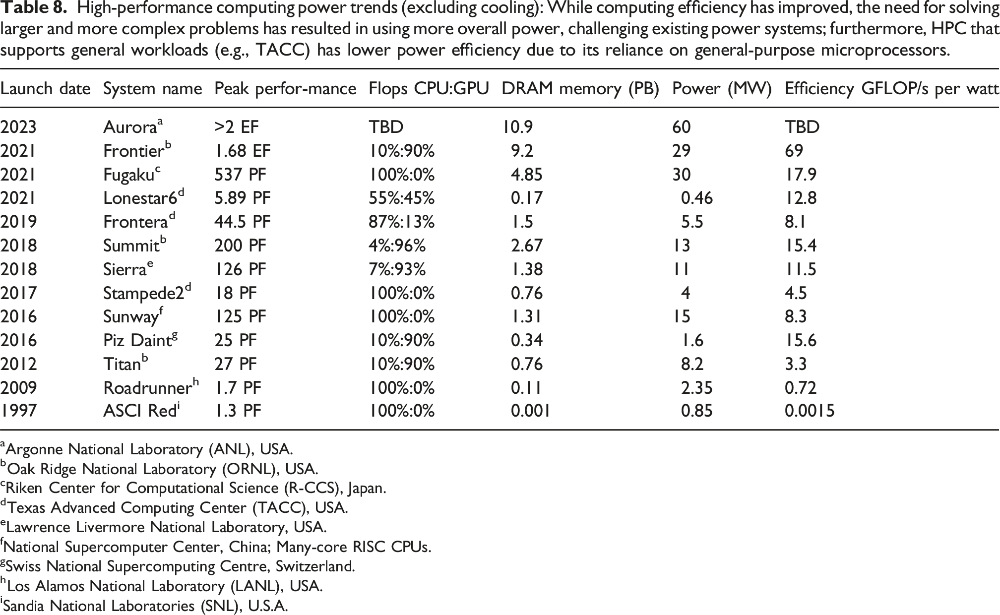
aArgonne National Laboratory (ANL), USA.
bOak Ridge National Laboratory (ORNL), USA.
cRiken Center for Computational Science (R-CCS), Japan.
dTexas Advanced Computing Center (TACC), USA.
eLawrence Livermore National Laboratory, USA.
fNational Supercomputer Center, China; Many-core RISC CPUs.
gSwiss National Supercomputing Centre, Switzerland.
hLos Alamos National Laboratory (LANL), USA.
iSandia National Laboratories (SNL), U.S.A.
Energy efficiency due to improvements in hardware
Energy efficiency of hardware resources depends on many factors, such as architecture, utilized technology, and software optimizations. Newer chips and servers have an ever-increasing power density. At the same time, due to the increased number of transistors per die, as well as ongoing architectural optimizations, computational throughput has greatly increased over time. Accordingly, while the latest devices have higher power demands, they exhibit improved energy efficiency.
Table 8 shows peak performance, power consumption, and energy efficiency for some of the world’s most powerful supercomputers 172 over the past two decades. It shows energy efficiency has improved over the years, whereas the total power consumption has increased. For instance, TACC’s Frontera (Stanzione et al., 2020) is 80% more energy efficient compared to TACC’s Stampede2 (Stanzione et al., 2017), but uses about 40% more power.
Clusters that extract more floating-point performance from GPUs (rather than CPUs) are more energy-efficient, as can be seen by comparing ORNL’s Frontier (2021) to Fugaku (2021), where Frontier is about 4 times more efficient. Some clusters, however, continue to rely heavily on CPUs or multi-core processors due to the flexibility they provide. This trend is particularly favored by some academic institutions and industries that primarily rely on scientific computing, have diverse workloads, and deal with complex legacy software that may not be easily ported to GPUs. Representative clusters of this category are Roadrunner (2009), Stampede2 (2017), Frontera (2019), and Fugaku (2021) (Table 8); energy efficiency of these systems has improved by about 20 times over the past 14 years.
Energy efficiency due to improved cooling systems and reduced overheads
Several metrics have been proposed for measuring the overall energy efficiency of a datacenter (Shao et al., 2022). One of the most widely-used metrics is Power Usage Effectiveness (PUE):
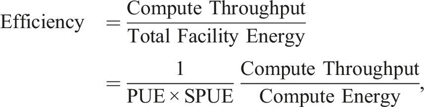
A large variety of cooling systems have been proposed and deployed, such as air cooled, air chilled, liquid cooling, and free cooling, leading to a large variation of attainable datacenter PUE. While the average datacenter PUE in 2022 was 1.55, according to the Uptime institute’s global datacenter survey, large-scale, state-of-the-art data centers achieve PUEs below 1.2 nowadays (Barroso et al., 2019). For instance, Google has been achieving a fleet-wide PUE average of less than 1.1 since 2020.
Interplay between future computing centers and the power infrastructure
Considerable energy demands of modern clusters and data-centers have significant implications, highlighted below.
Upgraded power infrastructure
The large power required by modern computing centers typically imposes a heavy load on the power grid. Sometimes, this requires upgrading and expansion of the power infrastructure (e.g., power grid and transformers), which could be complicated and costly. For instance, 2.5 mile-long power lines connected to the nearest power plant had to be installed in order to power Frontier.
Transition to lower-carbon and renewable energy
Some companies attempt to reduce their carbon footprint by powering their computing centers with lower-carbon and renewable energy sources. For instance, Google’s data-centers operate at over 67% on renewable energy (Harkness, 2023), with setting a goal to run on 100% lower-carbon energy by 2030.
Data-centers near nuclear power plants
To use more reliable, efficient, and low-carbon energy sources, data-center companies are examining nuclear energy as a power source for the near future. Current projects consider proximity to an existing nuclear power plant. In January 2023, Cumulus Data completed a 48 MW data-center shell, which is directly powered by the 2.5 GW Susquehanna nuclear power plant station in northeast Pennsylvania (Chernicoff, 2023).
Small modular reactors (SMRs) for data-centers
Compared to conventional nuclear power plants, SMRs are much smaller in size, allowing them to be portable. An SMR can typically provide between 50 MW and 300 MW of power. Recent advances in SMRs motivate placing them near large data-centers. There is currently about 80 commercial SMR designs under development worldwide. However, data-center companies are still unsure as to how they will perform in practice, and how the operating costs will be affected.
Some companies (e.g., Microsoft) are planning to install and deploy SMRs to power their data-centers in the future (Bradstock, 2023). NuScale Power is the first company that designs SMRs to receive approval by the U.S. Nuclear Regulatory Commission (NRC), and is planning to power two new data-centers in Ohio and Pennsylvania (Larson, 2023).
Impacts on high-performance scientific computing
For a long time, continuous improvements in computing hardware resulted in less pressure on many scientific computing applications to fundamentally reconsider their underlying algorithms. During this era, performance was significantly improved through increasingly more powerful processors as a result of technology scaling. Many applications also realized higher performance through parallelization, either via multi-core processors or multi-node computing. Concurrently, new algorithms, such as fast Fourier transform (1960s), multigrid (1970s), the fast multipole method (1980s), sparse grids (1990s), H matrices (2000s), multi-level Monte Carlo (2000s), and randomized matrix algorithms (2010s), considerably reduced the computational complexity of their predecessors (Dongarra and Keyes, 2024).
Even compared to 10 or 15 years ago, the hardware technology has changed strikingly: (a) number of cores within a chip has increased significantly, which makes finding opportunities for (within-the-chip) parallelization even more important; (b) the capacity of processors to crunch numbers have outpaced their ability to fetch data from off-chip memory, which puts greater emphasis on communication-reducing algorithms; (c) existence of different types of off-chip memory technologies invites novel algorithms for efficient data orchestration between the different memory components and the processing units; (d) energy efficiency considerations are driving heterogeneous computing, making accelerators, general-purpose processors, and other devices that exist on a computing system increasingly more diverse, which then makes efficient data orchestration between these components more challenging; and (e) AI’s large market size has popularized GPUs, and currently, is the primary driver of custom hardware development. While these aspects aimed to boost performance through various means, they have introduced new challenges that will not go away with time; they will likely get worse.
Furthermore, as technology scaling 174 is tapering, it will no longer deliver considerable improvements in performance. Accordingly, Shalf (2020) suggests meaningful performance gains may be realized through: (a) designing hardware-friendly algorithms in order to harness an existing hardware more effectively; (b) designing specialized hardware for certain algorithms or applications (Part I: Examples of custom and specialized hardware (Hanindhito et al., 2026)); however, this approach typically involves making changes to the underlying algorithms as well and is therefore closely related to (c) hardware-algorithm co-design, where hardware and the underlying algorithms or applications are designed together to maximize performance, including energy efficiency (Krueger et al., 2011). Hardware-algorithm co-design could be challenging, as it demands significant research and development efforts. Consequently, it may be adopted by limited groups within the scientific computing community that may be able to provide sustained funding to such undertakings, such as those who design and construct leading-edge high-performance computing systems (Reed et al., 2023).
Through a techno-economic analysis, Thompson and Spanuth (2021) argue that only applications with a high-value market can afford the R&D investments needed for specialization and thus be in the ‘fast lane’; applications with a small market size will be in the ‘slow lane’ and have to contend with slowly-improving CPUs. This is ominous news for those scientific computing applications that may not have a high-value market.
Lastly, we refer to a thought-provoking article by Matsuoka et al. (2023) for a different presentation style and perspective on where high-performance computing is heading before sharing our own. The authors discuss diverse topics such as hardware accelerators, extreme specialization, cloud, zettascale, and quantum computing, among others.
In the remainder of this section, we highlight the diversity that exists in scientific computing software, along with associated challenges. We then feature several options with varying levels of R&D effort, which promise to effectively harness modern hardware to deliver improved performance.
Software diversity in scientific computing
Numerical linear algebra, numerical solution of ordinary and partial differential equations (PDEs), and numerical optimization, frequently occur in many applications. Each of these branches have many variations, making scientific computing very diverse.
For instance, industry-relevant, large linear systems of equations are often sparse. Each particular application lends a specific mathematical structure to the linear system. Exploiting this structure in the utilized algorithm often improves performance. For instance, when a steady-state stress analysis in the automotive industry involves many different components 175 , the resulting linear system of equations offers some properties and structure to exploit. These include sparsity, positive-definiteness, and likely a large condition number due to the considerable differences in the stiffness matrices of the various components. In these situations, sparse direct solvers are often used due to their robustness. Often times, this step takes a significant portion of the total simulation time. Unfortunately, sparse direct solvers do not scale well on parallel computing systems. On the other hand, fluid dynamics simulations in the automotive industry, aimed at minimizing drag, lend a different structure to the linear system of equations. This allows using sparse iterative solvers, which scale better on parallel computers. However, effective utilization of iterative solvers often involves exploiting problem-specific mathematical structures in the adopted algorithm, which may include designing a customized preconditioner.
Similarly, industry-relevant partial differential equations are also very diverse. For instance, numerical solution of the acoustic and elastic wave equation dominates the computing resources of the oil and gas industry, and often relies on explicit, high-order finite differences, which scale well on parallel computers. Porting algorithms of this type to GPUs results in performance gains, and is becoming more common. On the other hand, unstructured-mesh-based PDE solvers that are used for hurricane storm surge predictions typically rely on low-order finite elements for robustness. They also have complex workflows 176 . Moreover, they involve solving a large, sparse linear system of equations, often through an iterative scheme. The utilized algorithms are mostly suited for multi-core CPUs. Porting these algorithms to GPUs, in a way that leads to meaningful performance gains, is extremely challenging.
Numerical optimization is commonly used in scientific computing. Some mathematical optimization schemes, such as the branch-and-bound method for mixed-integer nonlinear optimization, do not exhibit a faster runtime when parallelized (Maher et al., 2021). Therefore, there is little to be gained by porting them to GPUs, or multi-core processors. Performance gains in this area has often been enabled by improved algorithms. Gradient-based optimization schemes 177 often inherit a good portion of the structure of their associated underlying problem. For instance, industry-relevant gradient-based optimization schemes that are applied to the wave equation for oil and gas discovery parallelize well on modern architectures, such as multi-core processors and GPUs. They typically involve a significant memory footprint 178 , which requires careful data orchestration as one migrates from multi-core CPUs to GPUs 179 .
These examples, while not comprehensive, illustrate the diversity of algorithms that are encountered in scientific computing. Accordingly, a successful strategy that leads to meaningful performance gains necessitates careful analysis of the underlying algorithms of a specific application, their potential for parallelization, and their computational bottlenecks. Often, a commonly-used algorithm needs to be markedly revised to enable meaningful performance gains when executed on modern hardware. The diversity of scientific computing applications can hinder the securing of resources for such endeavors.
Challenges
We highlight some of the key challenges that hinder the adoption of modern hardware in scientific computing.
Old software
Many scientific computing applications rely on software that have been under continuous development for a long time. Some widely-used examples include: Computer-Aided Engineering (CAE) software packages, such as ANSYS, Abaqus, and Nastran; Earth system modeling packages, such as ADCIRC (Westerink and Luettich, 2024), MITgcm, and WRF (Skamarock et al., 2019); and software for molecular dynamics simulations, such as LAMMPS-MD (Thompson et al., 2022), GROMACS (Abraham et al., 2015), and NAMD (Phillips et al., 2005). These developments have been verified, extensively tested, and sometimes certified by regulatory agencies.
Changing the underlying algorithms of these software systems to make them attractive to modern hardware presents significant challenges. These include: (a) it is very difficult to extract performance from modern hardware (e.g., GPUs) if the underlying algorithms have low potential for parallelization, or if they have low arithmetic intensity 180 . For instance, many of the industry-favored algorithms use low-order discretization methods. Developing efficient, industry-attractive, high-order 181 discretization schemes require significant R&D efforts, and is often a high-risk, multi-year, multi-disciplinary endeavor; (b) migration of the workflow to modern hardware may not be a top priority due to resource limitations. Sometimes, a small part of the workflow gets ported to modern hardware (e.g., GPUs) as an exploratory step. However, migration of the entire workflow may be hindered; and (c) the re-certification process by regulatory agencies, if needed, could potentially be long and costly, and sometimes, it may discourage changing the underlying algorithms.
Flexibility vs. performance
Satisfying both flexibility and high-performance in scientific software is often challenging. By flexibility, we refer to the ability of a software package to take contributions from a large group of users, often scientists, who may not be well-versed in advanced coding. The flexibility allows users to make changes to the source code in order to implement functionalities based on their specific needs. Examples include LAMMPS-MD, which allows users to code their own potential energy function, and ADCIRC, where its algorithms have been under continuous improvement by computational scientists over the past decades. In addition, a top priority for a large-enough group of such users is productivity, which the tools support by allowing users to write code in C++ or Fortran 182 . This allows users to spend their time on testing ideas and algorithm development, rather than thinking about writing performant code on a non-general hardware platform, e.g., GPUs. Once the ideas and algorithms have been sufficiently tested on CPUs, they may find their way to a GPU code. Accordingly, some applications maintain a CPU code for productivity and development purposes, and a corresponding GPU version for performance. For instance, while LAMMPS-MD can run on GPUs for routine calculations, it still needs to run on CPUs for non-routine cases.
Poorly-parallelizable algorithms
Many industry-relevant applications rely on algorithms that do not scale well when more cores are available. A remarkable example is sparse direct solvers, which, often times, consume the bulk of the simulation time in CAE software. Developing algorithms that offer parallelizability, without compromising robustness, could be very challenging. Mixed-integer nonlinear optimization is another example where parallelization does not yield meaningful performance gains.
Scientific computing’s small market
Unlike machine learning and AI, many scientific computing applications have a small market size. This can sometimes make justifying investment decisions in the high-risk areas difficult. Some examples include migration of a complex workflow from CPUs to GPUs; and designing specialized hardware for specific applications (e.g., molecular dynamics for drug discovery, or wave simulation for oil and gas exploration). Making the situation even more difficult, it is often easier for ML and AI to attract top talent, thanks to their large and rapidly growing market, compared to scientific computing.
The large market size of ML and AI has a considerable impact on the scientific computing community, and is inspiring it to explore ways to ride the wave of ML and AI to manage investment costs. Examples include: solving PDEs on Cerebras’s large chip, which was primarily developed for ML applications (Part I: Examples of custom and specialized hardware (Hanindhito et al., 2026)); computational fluid dynamics (CFD) simulations on Tensor Processing Units (TPU) (Wang et al., 2022); and physics-informed ML, which often exploits GPUs. Nevertheless, these approaches have yet to become mature enough to be adopted for industry-relevant applications at scale.
Opportunities
Based on the level of effort one is willing to invest, there is some flexibility in how modern hardware can be used to improve performance. We highlight some of the most promising options next.
Leveraging modern hardware with minimal code change
This option could potentially be attractive to many academic researchers, as well as industry practitioners, since improving performance through making extensive algorithmic modifications may not be their highest priority. It may also appeal to old software that has been under development for a long time, and sometimes, may face difficulties in securing resources for code modernization. For instance, the Texas Advanced Computing Center (TACC) provides support for this approach through its CPU-heavy clusters (Table 8) in order to accommodate a diverse group of users. According to Stanzione (2022), Executive Director of TACC, less than 10% of TACC’s workload would work on Department of Energy (DOE) Oak Ridge National Laboratory’s Frontier, which is a GPU-heavy cluster (Table 8). The DOE has invested over a billion dollars on exascale codes, which primarily benefit extreme-scale applications that are intended to run on clusters similar to Frontier; however, the type of codes that run on TACC are largely different (Stanzione, 2022).
A successful strategy to improve performance under this approach requires a thorough understanding of the code, its execution flow, potential for parallelization, and memory footprint. Identification of hot-spots can provide insights on whether limited and targeted efforts directed at alleviating major bottlenecks can deliver meaningful performance gains. These low-effort options include targeting a small part of the code through: (a) limited algorithmic modifications; (b) using a modern external library 183 to perform the task of a hot-spot; and (c) offloading a compute-intensive hot-spot to a hardware accelerator.
Little can be done when a software has a complex execution flow, does not have a few distinct hot-spots, and offers limited opportunities to benefit from parallelization. Examples include sparse direct methods for solving a linear system of equations, and branch-and-bound method for mixed-integer programming. In these situations, a modern, low-core-count CPU 184 , with a high clock frequency, would likely result in a faster run-time. The low core-count allows for a higher power budget, which then permits higher clock frequencies. This enables higher single-thread performance. Furthermore, more cache per core is often available to modern, low-core-count CPUs. This typically helps applications that have complex execution flows. Lastly, a multi-core CPU with HBM can enable significant performance gains if the application is small enough to fit in the high-bandwidth memory.
For applications that already have been parallelized, but have a complex execution flow, using multi-core CPUs with a large amount of last-level cache could be most impactful in terms of faster run-time. If these CPUs are further equipped with HBM, they may enjoy faster run-times, as HBM may be used as a large last-level cache. Depending on the application, its arithmetic intensity, and the amount of intermediate computations that need to be kept near the registers, the desired amount of cache per core could vary. For applications with very high arithmetic intensity, a high-core-count CPU may deliver the highest run-time performance. Applications that have low arithmetic intensity with large amounts of intermediate results may benefit mostly from a low-core-count CPU that often provides more cache per core. Alternatively, to provide more cache per core, a high-core-count CPU may be used where not all cores are utilized. Larger applications may be impacted by inter-node communication. Oftentimes, a satisfactory configuration 185 that meets runtime, budgetary, and other desired metrics could be found through experimentation.
Leveraging modern hardware via considerable algorithmic changes
Some applications offer considerable opportunities for parallelization. These applications are at the forefront of algorithmic modification to harness modern hardware, if they are used by a large-enough market. Most likely, these applications have already benefited from parallel processing, multi-core, and many-core processors. Some examples include full-waveform inversion for oil and gas exploration, electromagnetic wave simulations for communication and defense applications, and molecular dynamics for drug discovery and material design. If these applications happen to have few canonical kernels, simple execution flow, and high computation to communication ratio, they become prime candidates for GPUs.
Next, we highlight several approaches that hinge on algorithmic modifications, resulting in a more effective way of harnessing modern hardware: (a) possible reformulation to increase arithmetic intensity, i.e., reducing data movement (Abduljabbar et al., 2017), perhaps at the expense of increasing local computation, e.g., through using different discretization schemes (Modave et al., 2015); (b) increasing locality to improve cache efficiency (Malas et al., 2015); (c) relaxing communication and synchronization constraints (Kumari and Donzis, 2020); (d) exploiting the growth in on-chip cores (Ang et al., 2014; Kogge and Shalf, 2013); (e) judiciously choosing the needed level of arithmetic precision at different parts of the code to alleviate communication bottlenecks and improve resource utilization (Abdulah et al., 2022; Croci and Giles, 2022; Croci and Rosilho De Souza, 2022; Goddeke et al., 2007; Haidar et al., 2017; Higham and Mary, 2022; Komatitsch et al., 2010); (f) selectively recomputing certain variables instead of storing them in memory, as the memory per core decreases; (g) simplification of the execution flow (Bielak et al., 2005); and (h) performing computations more efficiently, e.g., through using octree-based meshes (Burstedde et al., 2011; Rudi et al., 2015; Sundar et al., 2012), hierarchical algorithms (Abduljabbar et al., 2019; Keyes et al., 2020), and hierarchical matrices (Boukaram et al., 2018; Litvinenko et al., 2019).
Such algorithmic modifications are sometimes easier said than done for real-world applications. Generally, specific characteristics and needs of an application impede a straightforward implementation of a new algorithm into an existing framework. Typically, such endeavors involve multi-year, multi-disciplinary efforts for complex engineering applications.
Lastly, we point to the algorithmic Moore’s law suggested by Keyes (2023), where he observed an exponential rate of improvement for several algorithms that are fundamental in computational fluid dynamics and complex kinetics. Sustainment of such improvements has been viewed with caution by others; for instance, once an algorithm achieves linear complexity, there will be limited opportunities for further improvement (Matsuoka et al., 2023).
Leveraging developments in machine learning
Some algorithms, frameworks, or hardware that were originally developed for machine learning may also benefit scientific computing. A notable example is scientific machine learning (SciML), which refers to the solution of problems in scientific computing through leveraging data-driven approaches and/or techniques (e.g., automatic differentiation) that are typically used in machine learning. SciML methods are becoming increasingly popular in the scientific computing community. This popularity is primarily attributed to: (a) availability of many open-source ML-libraries and software, which significantly impact productivity; (b) ability of these methods to seamlessly incorporate data into first-principle-based models; (c) large market size of ML and AI, which impacts scientific computing 186 ; and (d) prevalence of GPUs in academia and industry compared to a few years ago.
Current SciML methods have mostly been applied to academic examples: they often consider one- or two-dimensional geometries and focus on proof-of-concept. Recently, there have been numerous attempts to incorporate complexities that exist in real-world problems, such as material heterogeneity, complex geometry, and richer physics. Some industries are also exploring the potential of SciML, including its ability to handle complexities that exist in real-world problems.
Oftentimes, SciML methods are not able to compete with traditional numerical methods in terms of accuracy and robustness in a classical sense. Nevertheless, this property is typically not needed for them to be impactful. Therefore, they are not expected to replace traditional techniques, such as the finite element method to solve PDEs. However, the ability of some SciML techniques to provide quick solutions to parameterized problems (e.g., PDEs that rely on a few input parameters) and to seamlessly incorporate observations, or other forms of data, make them attractive. SciML could possibly be leveraged in frameworks that rely on ensembles, such as uncertainty quantification, or inner loops of a multi-fidelity optimization scheme that can exploit fast but less accurate function evaluations (Ghattas et al., 2021). In other words, SciML will likely be most impactful in situations where accuracy can be compromised for speed, as well as in circumstances where data should be incorporated or its utilization lends robustness to the solution. Next, we highlight ML-based methods that have sparked considerable interest in the scientific computing community.
Physics-informed neural networks (PINNs)
In an influential work, Raissi et al. (2019) demonstrated how modern technologies in ML can be used to solve PDEs. They used neural networks to represent the solution space and automatic differentiation to readily compute partial derivatives in a PDE. A loss function, comprised of the PDE terms, along with initial and boundary conditions, is then minimized to compute the weights and biases of the associated neural network. The ability of the technique to enforce PDE terms, incorporate partial data (Karniadakis et al., 2021) and observations (e.g., in inverse problems), its simplicity due to exploiting automatic differentiation, as well as existence of software systems that allow others to test ideas quickly, continues to generate a lot of interest in the computational science community, resulting in many related works (Cuomo et al., 2022; Haghighat et al., 2021; Jagtap et al., 2020; Kharazmi et al., 2021; Krishnapriyan et al., 2021; Lu et al., 2021b; Penwarden et al., 2023; Yang et al., 2021; Yu et al., 2022).
Fourier neural operator (FNO)
The inspiring work of Kovachki et al. (2023) presents a technique for solving parametric PDEs, where a special neural network architecture, motivated by using Green’s functions to solve PDEs, is used to represent the numerical solution. The original technique uses sequential layers, where each layer performs discrete Fourier transform on the incoming input, discards higher modes, and then performs inverse Fourier transform, effectively filtering out higher frequencies. The Fourier transform is applied across all spatial dimensions, as well as in time, when applicable. FNO and its variants have been applied to a wide range of problems in scientific computing (Grady et al., 2023; Kovachki et al., 2023; Lehmann et al., 2024; Leinonen et al., 2024; Li et al., 2023b, 2024).
Deep operator network (DeepONet)
Lu et al. (2021a) proposed a special neural network architecture for solving parametric ODEs and PDEs, referred to as DeepONet. The approach is inspired by a theorem (Chen and Chen, 1995) that states a single hidden layer in a neural network is able to accurately approximate any continuous operator
187
. The architecture of DeepONet is directly motivated by the above-mentioned theorem, but with added layers for better expressibility. We highlight key characteristics of DeepONet by considering
Autoencoders (AEs)
Autoencoders are used for dimensionality reduction. They have similarities to the singular value decomposition (SVD) in the sense that both can be used to compress data by storing its most salient features. These salient features are referred to as singular vectors in SVD and latent-space vectors in AE. Nevertheless, SVD is a linear transformation, whereas AE can capture nonlinear relationships in data due to its reliance on neural networks. Specifically, an autoencoder takes input x, and maps it to the latent space z, through an encoder: z = E ϕ (x), where ϕ represents the parameters of the associated neural network. A decoder maps the latent-space vector back to the original space: x′ = D θ (z), where θ denotes the parameterization of the decoder. Parameters ϕ and θ are learned such that x and x′ are close to each other in some sense, and the dimension of z is much smaller than that of x. Several works (Kadeethum et al., 2022; Kim et al., 2022c; Wang et al., 2021b) have used autoencoders for reduced order modeling (ROM).
Variational autoencoders (VAEs) extend autoencoders by encoding the latent space as a probability distribution 188 rather than as fixed variables. The probabilistic latent space allows it to be sampled, which can then be used to generate new outputs through the decoder. Therefore, VAEs are known as generative models. This property may be used for image generation and data augmentation. Several works (Abubakar et al., 2022; Chen et al., 2023a; Lopez-Alvis et al., 2021), for instance, have used VAEs to generate new realizations of the subsurface geology that are consistent with a training dataset. The new realizations may then be used in parameter estimation and uncertainty quantification (UQ), among other applications.
Generative adversarial networks (GANs)
GANs (Goodfellow et al., 2014) can generate new data (e.g., images), or augment missing data, such that they share similarities with a training dataset. For instance, GANs have been used to generate new images of the subsurface geology (Feng et al., 2022; Miele and Azevedo, 2024; Puzyrev et al., 2022; Zhang et al., 2021) that have similarities with an available training dataset. GANs are comprised of two main components: a generator (G) and a discriminator (D), each typically being constructed with a neural network. G takes input from a latent space and transforms it to data that resembles the training dataset. D determines whether the generated data is statistically similar to the training dataset or not. The training continues until G can generate high-quality data in the sense that it becomes difficult for D to determine if the newly-generated data is produced by G or is from the original training dataset.
The latent spaces in GANs and VAEs are slightly different: a VAE enforces an explicit probability distribution (e.g., multivariate Gaussian) for its latent space, whereas the probability distribution of a GAN’s latent space is general and learned from data. Lastly, GANs are able to generate sharper images than VAEs due to using a discriminator in training.
Normalizing flows
Normalizing flows can improve the expressibility of the latent space in VAEs and GANs, among other things (Kobyzev et al., 2020). They are invertible functions that map a simple probability distribution (e.g., a multivariate Gaussian) to a more complex (e.g., multi-modal) distribution, where the latter is better suited to model complex relationships (Papamakarios et al., 2021). The invertibility property enables a two-way mapping between the latent space and the data space. Consequently, a straightforward statistical sampling in the latent space from a simple distribution can be mapped to the data space. On the other hand, mapping transformed data back to the latent space enables exact density estimation and computing the likelihood of observed data under the model. Some problems in scientific computing, such as probability density estimation (Maeda and Ukita, 2023), and variational inference (Rezende and Mohamed, 2015), can benefit from ML-based techniques that use normalizing flows, among other applications (Albergo et al., 2019; Köhler et al., 2020; Noe et al., 2019).
Transformers
Transformers (Vaswani et al., 2017) are predominantly used in natural language processing (NLP) for language translation, text summarization, and sentiment analysis. They can capture long-term dependencies within a sequence (e.g., text) through a mechanism called attention, which measures similarities between each two entries in the sequence. At a high level, a transformer consists of an encoder and a decoder 189 . The encoder captures dependencies and relationships within the input sequence. The decoder takes the encoded representations from the encoder and generates contextually relevant output, step by step, using the previously-generated parts of the sequence as context. Detailed description of various mechanisms of attention is beyond the scope of this paper. A mathematically precise and clear description of transformers is given by Turner (2023). Due to their ability to capture long-term dependencies 190 , transformers have been used for data-driven operator learning of PDEs (Geneva and Zabaras, 2022; Li et al., 2023c; Zhou et al., 2024) and ODEs (Shih et al., 2025).
Diffusion probabilistic models (DPMs)
Diffusion probabilistic models (Ho et al., 2020), also known as diffusion models (Sohl-Dickstein et al., 2015), belong to the broader class of generative models, which can generate new data that are statistically similar to an associated training dataset. DPMs are widely used for image generation, image denoising, image inpainting, and improving image resolution (super resolution). Through a forward diffusion process, Gaussian noise is incrementally added to an input image, via a Markov process, effectively transforming the input image into pure noise. Subsequently, a reverse diffusion process learns how to remove the aforementioned noise and recover the original input image. Consequently, DPMs can take pure noise as input to generate data that is statistically similar to an associated training dataset. Diffusion models have been used as conditional probability density samplers for subsurface inference in geophysics (Ravasi, 2025; Stojkovic et al., 2024; Zhang et al., 2024), subsurface multi-physics monitoring (Huang et al., 2024), solving PDEs (Yang and Sommer, 2023), and improving the resolution of discretized solutions (Lu and Xu, 2024), among other applications.
Specialized hardware for ODEs and PDEs
Developing specialized hardware for solving ODEs and PDEs is becoming more attractive. Anton, a specialized chip and computing system which was designed to target certain large-scale ODEs in molecular dynamics, is a successful example.
Building specialized chips for solving PDEs is more challenging, as it entails more kernels, which depend on the specific PDE, the associated discretization scheme, and sometimes the targeted problem. Moreover, most industry-relevant PDE simulators are limited by memory bandwidth. This implies that, while building a specialized chip for a particular PDE may lead to substantial performance gains on a single chip, multi-chip systems that are needed to solve larger problem sizes may not carry on the same level of performance. Therefore, algorithmic modifications to alleviate the memory bottlenecks become even more important for these multi-chip systems. Oftentimes, a hardware-algorithm co-design approach is pursued in such circumstances where both the hardware and algorithm are specialized to deliver maximum performance.
FPGAs are typically used for prototyping the chip design, prior to implementing it on an ASIC. There are several research works that use FPGAs for solving PDEs with different numerical methods. The work presented in (Lindtjorn et al., 2011) accelerated finite element sparse-matrix solvers and 3D convolutions for acoustic waves. Some works use the continuous Galerkin finite element (He, 2010) and spectral element (Karp et al., 2021) methods, while others employ the discontinuous Galerkin (dG) finite element method on meshes with unstructured tetrahedral elements (Kenter et al., 2018, 2021), or meshes with structured hexahedral elements (Gourounas et al., 2023). These works showed promising results against reference implementations on CPUs and GPUs. The FPGA design in (Lindtjorn et al., 2011) outperformed CPUs and GPUs by up to 70× and 14×, respectively, while the one in (Kenter et al., 2021) outperformed the reference CPU implementation by 43× to 144×. Moreover, the accelerator in (Gourounas et al., 2023) achieves 4.27× higher throughput than 24 Xeon CPU cores, with 31.33× higher energy efficiency. However, it does not utilize HBM, showcasing suboptimal scalability with memory bandwidth. In a later work (Gourounas et al., 2025), the authors extended their design to HBM-enabled FPGAs, outperforming GPUs by up to 48%, with up to 2.84× higher energy efficiency. Additionally, in (Gourounas et al., 2023, 2025), the proposed dataflow and architecture can support a plethora of hyperbolic PDE solvers under the dG scheme, by simply making minor changes to the HDL code (Part I: Implementation choices (Hanindhito et al., 2026)) and reconfiguring the FPGA. Such approaches can be reinforced with the use of custom HDL generation tools, thus minimizing programmability overheads of the FPGA accelerators. Therefore, FPGAs can achieve much higher flexibility than ASICs, while showing higher energy efficiency compared to CPUs and GPUs (Boutros et al., 2020; Gourounas et al., 2023, 2025; Zhuang et al., 2023) As a result, FPGAs are a challenging hardware platform candidate for PDE solvers, where the large diversity of compute kernels and their possibly continuous evolution imposes severe challenges to the design of ASICs that can support a large number of applications.
Overall, the main disadvantages of FPGAs compared to GPUs include longer and more complex development cycles, as well as much lower available memory bandwidth 191 . The latter can become a major performance bottleneck for many memory-bound HPC workloads (Gourounas et al., 2023; Hanindhito et al., 2022). Nevertheless, as FPGA software support matures and approaches like programmable overlays (Fowers et al., 2018) become more popular, the productivity gap between the two is expected to become smaller. Moreover, as FPGAs evolve to more advanced technology nodes, and faster HBMs are integrated on the same package, higher clock frequency and memory bandwidth will become available at even better power envelopes 192 .
We are not aware of a publicly-known ASIC that was specifically built for solving PDEs. Nevertheless, there are a few examples of using machine learning chips that were also used to solve PDEs (Part I: Examples of custom and specialized hardware (Hanindhito et al., 2026)). These examples required significant effort to map the PDE to the specialized hardware, and sometimes needed algorithmic modifications to address bottlenecks. These examples demonstrate significant performance gains as along as the problem size fits into a single chip. Off-package communication severely degrades the run-time performance when several packages have to communicate in order to target larger problem sizes.
While an ASIC designed specifically for solving PDEs could yield higher performance and energy efficiency compared to other hardware platforms, it may not always be the most viable approach. PDE solvers could include a wide variety of equations, discretization schemes, computational details, and dataflows. To support a sufficiently large group of applications, an ASIC must be designed to be highly programmable, which brings additional overhead. Even then, different applications will exhibit different problem sizes or arithmetic intensities. Designing the ASIC to account for the worst case scenario can lead to the severe under-utilization of the hardware in some applications. For instance, imagine an ASIC that can handle both the acoustic and elastic wave equation. The elastic wave equation has more variables, and entails more intermediate computations. Therefore, the specialized memory and compute units of this ASIC need to be carefully balanced (designed) to maximize desired performance metrics. The acoustic wave equation would need a different balance to be optimal. Therefore, an ASIC that is aimed to handle both would be suboptimal.
Emerging computing technologies
The slowdown in Moore’s law and the growing computational demands of today have spurred the development of alternative 193 approaches to computing, whose potential impact cannot be understated. Leveraging specific physical characteristics of a system, such as high-speed transmission in photonic computing or the storage capacity of DNA molecules in DNA computing, to perform computational tasks may unlock innovative solutions to complex problems. More established emerging paradigms such as quantum computing and physical annealing hold promise for revolutionizing computational endeavors across many application domains. Quantum computing’s innate ability to efficiently model complex quantum systems, that are difficult or impossible to simulate with classical approaches, make it particularly well-suited for addressing challenging problems in physics and chemistry. Physical annealing techniques offer a unique approach to optimization tasks by mimicking physical processes to find globally optimal solutions, with applications ranging from chip design to protein folding. When seamlessly integrated with traditional high-performance computing architectures, these novel technologies can serve as potent accelerators, propelling computational science into uncharted realms of discovery and innovation.
It is imperative to acknowledge that while promising, these novel technologies are still in nascent stages of development and not yet fully matured. Despite this, their impending emergence underscores the significance of proactive recognition within the computational science community. By embracing and adapting to the evolving landscape of computational technology, practitioners can position themselves at the forefront of innovation, poised to harness the transformative potential these advancements offer. This forward-thinking approach not only fosters a culture of adaptability but also ensures that practitioners are primed to capitalize on the unparalleled opportunities that lie ahead in the realm of computational science.
Practitioners within the field of computational science are urged to discern and embrace the fluid trajectory of computational technology, strategically harnessing external advancements for maximal efficacy.
Outlook
If the future of computing could be summarized in two words, they would be specialization and diversity. As technology scaling reaches its limits, improvements in performance will increasingly rely on exploiting the specifics of an application. This entails building hardware that is specialized for a specific application, or a class of similar applications, as well as designing algorithms that exploit properties and structures of the specified application and also adapt to modern hardware. This approach is known as hardware-algorithm co-design.
This paradigm has generally been embraced in ML/AI: there are several examples of specialized hardware for AI, not to mention GPUs, which have emerged primarily due to the large market size of AI and its rapid growth 194 . Adapting to modern hardware, a large number of ML algorithms enjoy high arithmetic intensity, use multiple levels of precision to use resources more efficiently, and strive to reduce their communication bottlenecks. Sometimes, these algorithmic adaptations result in loss of accuracy in a classical sense. However, many ML/AI algorithms may be able to tolerate this loss of accuracy, as statistical accuracy may be sufficient for many applications. One may observe that on the one hand, ML/AI are adapting to technology trends in modern hardware; on the other hand, hardware manufacturers are influenced by the large market size of ML/AL. This has led to a virtuous cycle, resulting in growing number of new hardware products that are more suited for ML/AI than other applications. We refer to the insightful works by Reed et al. (2023) and Thompson and Spanuth (2021) for detailed perspectives on how big tech companies are influencing the computing industry.
Embracing this paradigm in scientific computing is more challenging. Scientific computing has a smaller market size with a modest projected growth, which impacts R&D investments. Moreover, traditionally, scientific computing has dealt with calculations that were expected to be accurate in a classical sense, where consequences of inaccuracies could be significant. This makes algorithmic relaxations more challenging for many scientific computing applications. Nevertheless, technology trends in hardware cannot be ignored, and scientific computing is responding in several ways. Some examples include: (a) growing number of scientific computing applications that run on GPUs; (b) active research on algorithms that better adapt to modern hardware, such as high-order discretizations, mixed-precision calculations, and communication-reducing algorithms; (c) exploring ways to incorporate ML-based techniques in traditional scientific computing frameworks; (d) designing specialized hardware for certain applications; and (e) running scientific computing applications on specialized hardware that was primarily designed for ML. These trends are expected to continue. Some options, such as hardware specialization, may become less costly due to the emergence of open-source, automated design tools.
Not all applications can follow the main technology trends, either due to inherent complexities within their algorithms, or lack of needed resources for software modernization. These applications will continue to run on CPUs, and will likely benefit from higher clock frequencies, and larger on-chip (and on-package) memory capacity of certain multi-core CPUs.
Energy efficiency will be the central theme in hardware design for the years to come. While computer designers strive to improve energy efficiency, the quest to run more, larger, and more detailed models is resulting in larger computing centers with a growing energy demand. In some cases, this level of growth in energy demand was not anticipated when large computing centers were built. Therefore, their expansion may necessitate upgrades in the power grid infrastructure. Large computing centers in the future may even rely on small modular nuclear reactors as a reliable source of energy.
Access, or lack of access to cutting-edge technology will impact computing for the years to come, and will likely lead to more diversity. For instance, when access to advanced process node technology is regulated, performance may rely more on hardware specialization. Sunway Taihulight (Table 8) is a notable example. The future of scientific computing is inevitably more diverse and more challenging than its past. This provides new opportunities to computational scientists.
Frequently asked questions
We end the paper by answering several questions that are often asked by managers, decision makers, and practitioners: What are some quick options to improve the performance of a large and old software that took decades to develop?
The answer requires investigating whether the old software is highly parallelizable, how much it may benefit from parallelization, and how complex are its control flows.
If the software does not gain much from parallelization and has complex control flows, using modern low-core-count CPUs might lead to the fastest runtime, as it allows higher clock frequency, and has higher on-chip memory per core.
If the application scales well on parallel systems but has complex control flows, a modern multi-core CPU may enable the fastest runtime. Specifically, if the application involves many intermediate computations and data, a low-core-count CPU may work best, as it provides more on-chip memory per core. Alternatively, if the application has few intermediate calculations and needs little data to operate on, a high-core-count CPU could be more appropriate. Using modern high-core-count CPUs and turning off some cores to provide more on-chip memory per active core is also an option if needed.
If the application parallelizes well, and has simple control flows, migration to GPUs may provide more speedup compared to using multi-core CPUs. It could be costly and time-consuming, and thus performance gains need to be large enough to justify the effort.
In all these cases, using high-bandwidth memory (HBM) will likely make the application run faster, as it improves on-package bandwidth, and increases memory capacity near the compute units. Lastly, if inter-node communication is the main bottleneck, partitioning the problem according to the network topology, or using a network interconnect that has a higher bandwidth would likely help. Inter-node communication is limiting the performance of an important application. Can the bandwidth be increased by adding more (InfiniBand) “cables” between the nodes?
Inter-node bandwidth can be increased by adding more NICs to each node and connecting them to the network. This forms a multi-rail network (Coll et al., 2001), and has been used in high-end clusters that run multi-node machine-learning applications.
This approach faces three main challenges: (a) it is very expensive; (b) since processors are pin-limited (Part I: Off-chip interfaces and pin limitations (Hanindhito et al., 2026)), there is a limit on how many NICs can be placed on each node; and (c) there is a limit on how much bandwidth a network switch can handle, which translates to how many network endpoints the switch can serve. With each node needing multiple connections, the number of switches needed will skyrocket. Not only this is expensive, it also necessitates using higher-order level switching that imposes certain topologies (Network topologies). This also makes it more difficult for communication libraries to optimize communication patterns.
It is possible for the network topology and configuration to be reasonably specialized in order to provide higher bandwidth to a certain group of applications. We consider two cases to further clarify this point. In the first case, most of the jobs on a cluster may not be extremely large, and only need a few nodes to run. This is a common situation for many applications in industry and academia. For instance, full-waveform inversion for oil and gas exploration falls into this group. To benefit these applications, the network can be designed to provide higher bandwidth and low latency communication for the nodes in the same rack through using top-of-the-rack switches. However, the job scheduling algorithm must carefully allocate the nodes on the same rack. The small-multi-node simulations then may be restricted to run on compute nodes within the same rack. Spine and super-spine switches are then used to connect all top-of-the-rack switches. However, they are often over-subscribed, and thus, bandwidth between racks may not be as high as bandwidth within a rack. The second case involves specializing the network topology to the communication pattern of a specific problem in order to limit inter-node communication bottlenecks. This option may be considered when a cluster is primarily used to run a single application: an unlikely situation in academia, while possible in some industrial applications. Molecular dynamics (MD) simulations for drug discovery by the pharmaceutical industry, and solving PDEs through domain decomposition fall into this group. In this case, each node may be connected to its six neighbors to form a 3D torus network topology. This topology follows the pattern that atoms interact with each other in the physical space, and therefore, minimizes communication bottlenecks. The Anton specialized computing system for MD simulations uses this network topology. The downside of this design is that the cluster could become much slower for applications that do not follow this communication pattern. How to choose the most suitable computing platform (CPU, GPU, ASIC) for a specific application?
The selection of the hardware platform depends on a variety of factors, such as productivity or development rate, cost, flexibility, performance constraints and/or power budgets. CPUs are great for software development, and algorithmic debugging and exploration, since they are easy to program and fully flexible. However, they may not be an ideal choice for a competitive end-product, due to their high inherent programmability overheads, which greatly limit their attainable throughput and energy efficiency compared to other alternatives.
GPUs are a better alternative for some applications, capable of outperforming CPUs by an order of magnitude. CPUs remain suitable for tasks within the workload that lack parallelization and entail complex control flows. Conversely, GPUs excel in handling the most computationally intensive and parallelizable kernels. However, despite their programmability, developing a GPU code is more challenging than CPUs, typically demanding a profound comprehension of the underlying architecture. Furthermore, GPUs come at a higher cost than CPUs, hence amplifying the budgetary needs for constructing a computing cluster.
The effectiveness of specialized hardware (ASICs) is contingent upon the specific deployment circumstances. Established computing kernels intended for deployment with minimal modifications over a long time-frame and adaptable across diverse applications are ideal candidates for ASIC development. Nevertheless, it is an expensive, protracted, and complicated endeavor. It necessitates the recruitment of highly skilled teams and individuals, along with substantial investments of time and capital, consequently elevating the total cost of ownership significantly. This aspect often dissuades non-tech companies from pursuing ASIC development. A comprehensive analysis, weighing all available alternatives, is imperative before committing to the design of specialized hardware. What are some key issues that should be investigated prior to developing specialized hardware for a specific application (e.g., solving PDEs)? What kind of performance improvements are expected?
First and foremost, an extensive performance analysis of the algorithm is required. What are the parallelizable portions of the code and what percentage of the total runtime do they constitute for? Do data dependencies limit parallelism and what is the expected runtime on a proposed hardware architecture (estimated via analytical modeling)? What are the communication bandwidth requirements to allow efficient utilization of the compute resources?
Next, the range of applications that the hardware should support must be considered, along with the evolution rate of the algorithms. These aspects will dictate the selection of architecture alternatives and how programmable the computation engines need to be. It would be hard to justify investing in a multi-year project that would likely cost tens of millions of dollars to develop a chip for an application considered outdated soon after it is manufactured.
Putting together a system that includes a hardware accelerator, the necessary peripherals and an extensive software stack necessitates the recruitment of expert teams comprising computer architects, hardware designers, silicon engineers, software engineers etc. Different teams will work on different aspects of chip development, such as RTL design, verification, physical layout and the software stack, among others. Finally, the selection of the manufacturing technology (e.g. TSMC, Samsung, Intel) and process will play a crucial factor in the device’s area footprint, performance and power envelope. Thorough verification and debugging through simulation are essential before tape-out. Any bugs or errors discovered post-tape-out lead to a complete repetition of the manufacturing process, substantially increasing manufacturing costs.
Regarding performance benefits, these depend on many factors, such as the size of the chip, the technology process, application characteristics and the architecture. In general, an ASIC can achieve one to two orders of magnitude higher performance compared to CPUs, and significantly outperform the GPU as well, unless the application is highly memory-bound, in which case the GPU may have a similar performance. This holds true in cases where the problem size can fit in one node. Large-scale problems that require multi-node deployment may be greatly limited by inter-node communication, thus negating the performance benefits of the specialized hardware.
An application-specific chip can also be orders of magnitude better than CPUs and GPUs in terms of energy efficiency, depending on the application characteristics mentioned above. However, some of its performance and efficiency must usually be sacrificed to enable some degree of programmability in order to support an adequate range of applications. Does the end of Moore’s law mean we will no longer be getting faster chips?
In the broader sense, the end of Moore’s law does not necessarily mean chips will not get faster anymore. Instead, the traditional methods of doubling transistor density every 2 years, at the same cost, as predicted by Gordon Moore in 1975, are no longer sustainable due to the physical and technological limitations (Part I: Transistor size and Moore’s law (Hanindhito et al., 2026)). Therefore, chip manufacturers are exploring alternative techniques in materials, lithography, advanced packaging, and architecture, to continue improving chip performance. This has increased the cost of designing and manufacturing the chips (Part I: Cost of designing and manufacturing semiconductors (Hanindhito et al., 2026)).
While specialized chips and hardware accelerators can enable significant performance improvements, general-purpose microprocessors will no longer see a significant jump in individual core’s performance. Improvements in CPU performance will primarily be due to more parallelism, enabled by using more cores. However, this will result in higher power consumption as well as higher manufacturing costs. Why should one be concerned about the increasing power consumption of modern chips if electricity bills are a small fraction of their expenses?
Aside from the increase in electricity bills, which may not be too significant in itself, the increasing power consumption of modern chips creates two major challenges: (a) supplying power to them becomes more difficult; and (b) cooling them becomes increasingly more challenging and expensive. Moreover, the growing energy demand of modern chips sometimes requires upgrading the power infrastructure for cluster-sized systems. Lastly, computing platforms are increasingly becoming a major portion of the global energy consumption. Therefore, taking merit in optimizing for computing energy efficiency becomes even more important.
Footnotes
Acknowledgements
Arash Fathi and Dimitar Trenev are grateful to ExxonMobil for supporting this work, and permitting its publication. We would like to thank Laurent White for stimulating conversations and commenting on an earlier draft of this paper, which improved its quality. We are also grateful to Amir Gholami, Arben Jusufi, Ardavan Pedram, Brent Wheelock, Chirath Neranjena, Dakshina Valiveti, Dimitri Papageorgiou, Rahul Sampath, and Wenting Xiao, for insightful conversations and feedback.
Funding
The authors disclosed receipt of the following financial support for the research, authorship, and/or publication of this article: This research was supported by ExxonMobil Research and Engineering Company, agreement number EM10480.36, Division of Computing and Communication Foundations (1763848) and National Science Foundation (NSF) grant numbers 2326894 and 2425655.
Declaration of conflicting interests
The authors declared no potential conflicts of interest with respect to the research, authorship, and/or publication of this article.
Disclaimer
Any opinions, findings, conclusions, or recommendations are those of the authors and not of the sponsors.