
Abstract
In the field of optical science, it is becoming increasingly important to observe and manipulate matter at the atomic scale using ultrashort pulsed light. For the first time, we have performed the ab initio simulation solving the Maxwell equation for light electromagnetic fields, the time-dependent Kohn-Sham equation for electrons, and the Newton equation for ions in extended systems. In the simulation, the most time-consuming parts were stencil and nonlocal pseudopotential operations on the electron orbitals as well as fast Fourier transforms for the electron density. Code optimization was thoroughly performed on the Fujitsu A64FX processor to achieve the highest performance. A simulation of amorphous SiO2 thin film composed of more than 10,000 atoms was performed using 27,648 nodes of the Fugaku supercomputer. The simulation achieved excellent time-to-solution with the performance close to the maximum possible value in view of the memory bandwidth bound, as well as excellent weak scalability.
Keywords
1. Introduction
Light–matter interaction is an essential topic relevant to the disciplines of physical and chemical sciences and optical and electrical engineering. The invention of the laser in early 1960s (Maiman, 1960) led to a number of innovations in these fields. Since then, laser technologies have developed in various directions.
One branch that has demonstrated rapid progress is the field of nonlinear and ultrafast optics, which has been developed along with a method for generating strong and ultrashort pulsed light. The method for generating an ultrashort high-intensity laser beam was awarded the Nobel Prize in Physics in 2018 (The Nobel Foundation, 2018). Ultrashort laser pulses can be used as a means of accurate measurement. In particular, it is possible to explore atomic and electronic motion in matter using laser pulses as short as several tens of attoseconds (10−18 s) (Krausz and Ivanov, 2009).
Strong laser pulses induce nonlinear light–matter interaction, which is the basis of various optical devices. Using strong pulses, it is possible to control and manipulate atomic and electronic motion in matter at a time scale as fast as several femtoseconds (10−15 s). Irradiation of intense and ultrashort pulsed light has been utilized for laser surgery and processing. Nonthermal processing using femtosecond laser pulses is expected to play a central role in future manufacturing applications (Malinauskas et al., 2016).
An integrated technology utilizing nano and laser technologies is another active field of optical sciences, known as nano-optics or nanophotonics (Schuller et al., 2010). Utilizing the characteristic properties of electromagnetic fields that appear around nanosized materials, a number of new concepts and fields have been developed, including near-field optics, plasmonics, metamaterials, and metasurfaces.
Phenomena relevant to light–matter interaction are multiphysics in nature, involving the propagation of light waves and the dynamics of electrons and ions in matter. Three physical laws are involved there: electromagnetism for light fields, quantum mechanics for electrons, and Newtonian mechanics for ionic motion. The phenomena are also multiscale. In terms of length, the typical wavelength of a light wave is approximately 1 micrometer (10−6m), while the motion of electrons and ions is measured in nanometers (10−9m) or less. In terms of time, periods of light and electronic excitations are typically measured in femtoseconds (10−15s), while atomic motion is measured in picoseconds (10−12s).
Due to the multiphysics and multiscale nature of the problem, two separate computational approaches have been developed. The first is electromagnetic analysis, in which matter is treated as continuum media, and the second is ab initio quantum-mechanical calculation of the optical properties of materials. These two approaches assume weakness of the light field (perturbation theory in quantum mechanics) and difference in the length scale (macroscopic electromagnetism). However, the usefulness and capability of these traditional computational approaches are limited in current research.
In this paper, we describe our attempt to develop an ab initio and unified simulation method for light–matter interaction. This method involves a coupled simultaneous calculation of electromagnetic analysis for light electromagnetic fields, ab initio time-dependent density functional theory (TDDFT) for electron dynamics, and molecular dynamics for ionic motion. The development of scalable and efficient code is essential to achieve this simulation.
We then examine the size and time scales encountered in practical problems. When pulsed light irradiates a bulk material, the surface often plays an important role. The emission of electrons and ions may occur on the surface, and the electronic structure at the surface often differs from the bulk system. It is thus essential to calculate materials that are several nanometers thick (several tens of layers of atoms) from the surface to investigate light–matter interaction in materials. As an illustration, let us consider a cubic nanoparticle composed of 103 atoms. In this system, about a half of atoms are exposed to the vacuum since 83 = 512 atoms are inside. Since atoms in the second layer behave also differently from the bulk material, optical responses of nanoparticles of 103 atoms are dominated by their surface properties. In a cubic nanoparticle of 203 atoms, about a half of atoms are in the first and second layers and remaining atoms (163) are inside. Therefore, to explore a competition of surface and bulk properties in optical responses of nanoparticles, we consider that it is essential to calculate nanoparticles composed of 104 atoms and more.
With respect to the time scale, periods of typical laser pulses and electronic excitations are characterized by several femtoseconds (10−15s). Ion motion is significantly slower than electron motion: the fastest phonon period is several tens of femtoseconds. The energy transfer from light to electrons occurs extremely quickly; however, the energy transfer from electrons to ions takes several hundreds of femtosecond to several picoseconds (10−12s). The time step used in our simulation is compared with these physical time scales. We utilize an explicit method in our calculation, and the time step is limited to approximately 1 attosecond (10−18s). Therefore, time evolution of 105 steps is required for a simulation with a 100-femtosecond duration.
To explore light–matter interaction, simulations as well as experiments comparing different physical conditions are required: a comparison of different laser pulses (frequency and intensity) and a comparison of different materials and structures. To perform several calculations in a reasonable period of time, it is preferable for a single calculation to be completed within at most 1 day. To complete 105 steps in 1 day, the calculation of a single time step should be completed in 1 second. This time-to-solution condition, 1 second per step, is the target of our implementation and optimization.
Once this time-to-solution is realized, our code will be readily applicable to phenomena that take place within 100fs. Although it is not sufficient for phenomena that involve structure changes of materials that usually take time longer than a picosecond, there are numerous optical and ultrafast phenomena in nanostructures and extended systems that our code will be useful. They include experiments using attosecond pulses that enable to explores electronic dynamics in matter in time domain (Krausz and Ivanov, 2009; Lucchini et al., 2016; Sommer et al., 2016), electronic excitations and linear optical absorption of nanomaterials (Noda et al., 2014b; Jornet-Somoza et al., 2015), extremely nonlinear optical responses such as high harmonic generations (Yamada and Yabana, 2021), energy transfer from laser pulse to electrons in matter (Malinauskas et al., 2016), coherent phonon generations and their detections (Yamada and Yabana, 2019), and so on.
We next review current state of the art of simulation methods for light–matter interactions. The method used in the present work is a combination of electromagnetic analysis for light electromagnetic fields and ab initio real-time TDDFT for electron dynamics with ionic motion described by Ehrenfest molecular dynamics. We first describe the state of the art of these two frameworks when used separately, and then the state of the art of the combined calculations.
The finite-difference time-domain (FDTD) method is a standard tool for analyzing the three-dimensional (3D) propagation of waves in electromagnetism and acoustics. In optical applications, Maxwell equations are solved in real-time and real-space for given distributions of materials and an initial configuration of electromagnetic fields. To perform parallel FDTD calculations, essential parallel algorithms using MPI were developed in 2001 (Guiffaut and Mahdjoubi, 2001). Since then, large-scale computations have been attempted for problems with complex geometric structures. Smirnov et al. (2014) reported calculations for problems of more than 1010 cells and up to 4096 nodes using Blue Gene/Q at the IBM Thomas J. Watson Research Center. It demonstrated good strong scalability up to 2048 nodes. In Lesina et al. (2017), Vaccari et al. reported calculations for nanophotonics involving a plane-wave incident on a gold nanosphere of radius 60 nm using 65,536 cores of IBM Blue Gene/Q.
Regarding ab initio electron dynamics simulation of materials, several approaches solving time-dependent Schrödinger-like equations have been developed. Time-dependent density functional theory is an extension of the ordinary static density functional theory (DFT) for describing time-dependent electron dynamics induced by external fields (Runge and Gross, 1984). It should be noted that there are two types of numerical implementations in practical TDDFT calculations. The first is the linear-response TDDFT in frequency domain in which linear algebraic equations are solved. The second numerical implementation is the calculation of electron dynamics solving the time-dependent Kohn-Sham (TDKS) equation in real-time as an initial value problem which is often called real-time TDDFT. Both methods are implemented in a number of codes in physics, chemistry, and material sciences. In the present study, we employ the real-time TDDFT for phenomena in which electronic states during the time evolution can greatly differ from those in the ground state.
Real-time TDDFT calculations began in the 1990s (Theihaber, 1992; Yabana and Bertsch, 1996; Bertsch et al., 2000). For large-scale computations, a 3D grid method for the spatial variable is often used to solve the TDKS equation. The same grid representation is also often used in large-scale calculations of ordinary static DFT (Chelikowskhy et al., 1994). For example, using real-space DFT (RSDFT) (O(N3) real-space grid code for static DFT), a system composed of 100,000 atoms was calculated, receiving the 2011 Gordon Bell prize (Hasegawa et al., 2011).
As an open source software based on real-time, real-space TDDFT, OCTOPUS (Andrade et al., 2012) has been widely utilized. OCTOPUS incorporates parallelization by dividing the spatial region as well as orbitals. Using OCTOPUS, calculations of a system composed of 2676 atoms using 16,384 cores of Blue Gene/P at the Rechenzentrum Garching of the Max Planck Society, Germany, have been reported (Andrade et al., 2012). A calculation of linear optical responses of biomolecules with more than 6000 atoms has also been reported (Jornet-Somoza et al., 2015). Calculations have also been reported using GCEED, another real-time, real-space program (Noda et al., 2014a), for a molecular crystal of C60 fullerenes composed of 1920 atoms (7680 electrons) using up to 7920 nodes (63,360 cores) of the K-computer, RIKEN-AICS, Japan (Noda et al., 2014b).
In 2016, large-scale electron dynamics calculations of DC conductivity in a disordered aluminum system (consisting of 5400 aluminum atoms that included 59,400 electrons) were achieved using 98,304 nodes of Sequoia Blue Gene/Q at LLNL. It demonstrated good scaling up to the largest computation, and a performance of 8.75 PFLOPS was recorded (Draeger et al., 2016). This calculation uses a plane-wave basis. Using the plane-wave basis, the most time-consuming part is the operation of the norm-conserving pseudopotential (PP) that is performed as operations of dense-matrix multiplication and is accelerated using BLAS dgemm and zgemm.
Last year, a large-scale real-time TDDFT calculation with the hybrid functional was reported using Summit at ORNL (Jia et al., 2019). Using the hybrid functional, the dominant calculation becomes the operation of the nonlocal exchange operator on electron orbitals that scales as O(N3). The implementation was demonstrated to scale up to 786 GPU for a system with more than 1000 atoms.
The above-mentioned large-scale real-time TDDFT calculations all describe electron (and sometimes ion) dynamics for a given external field. When electromagnetic fields of light propagate in a medium, however, electron motion induced by the field, known as polarization, modifies the field itself. To account for this effect, it is necessary to consider the coupled dynamics of electrons and electromagnetic fields. Multiscale modeling combining macroscopic Maxwell equations and microscopic Schrödinger-like equations has been developed for the propagation of pulsed light in a gas medium (Lorin et al., 2007), in molecules and nanoparticles (Lopata and Neuhauser, 2009; Chen et al., 2010), and in crystalline solids (Yabana et al., 2012). Large-scale calculations in multiscale modeling have been explored using ARTED (ARTED Developers, 2016). This code solves the time evolution of 3D Bloch orbitals at the microscopic scale and the one-dimensional propagation of electromagnetic fields of pulsed light.
ARTED has been successful in analyzing optical experiments utilizing attosecond technology (Sommer et al., 2016; Lucchini et al., 2016). Calculations reported in Sommer et al. (2016) were performed using the K-Computer, RIKEN-AICS, Japan. A typical single production run required 19 hours using 8000 nodes (64,000 cores). In Hirokawa et al. (2018), coupled calculation of 3D Maxwell and 3D TDKS using ARTED was reported. The calculation was performed using almost all 8192 nodes of the KNL processors of Oakforest-PACS at JCAHPC, and a 12–16% performance was obtained.
In the present work, SALMON (Scalable Ab Initio Light Matter simulator for Optics and Nanoscience) code (Noda et al., 2019) is used. SALMON has been developed by the present authors unifying two codes, ARTED and GCEED, both of which were developed for the large-scale calculation of real-time TDDFT.
2. Simulation method and implementations
2.1. Basic equations, grid system, and algorithms
We simultaneously solve Maxwell equation for the scalar and vector potentials of electromagnetic fields, the TDKS equation, the basic equation of TDDFT for electron motion, and the Newton equation for ionic motion. A detailed implementation of the method is explained for the coupled dynamics of electromagnetic fields and electrons in Yamada et al. (2018), and for the coupled ionic motion in Yamada and Yabana (2019).
The ab initio description of electron dynamics is the core of our simulation in both theoretical and computational points of view. The electron orbitals ψ
b
(
The ionic coordinates
Electromagnetic fields follow Maxwell equations. The scalar potential ϕ satisfies the Poisson equation in the Coulomb gauge with the charge density of electrons and ions. The vector potential
A practical procedure to solve the equations is summarized as a flowchart in Figure 1. The flowchart of the calculation as well as numerical methods and dominant communications are summarized.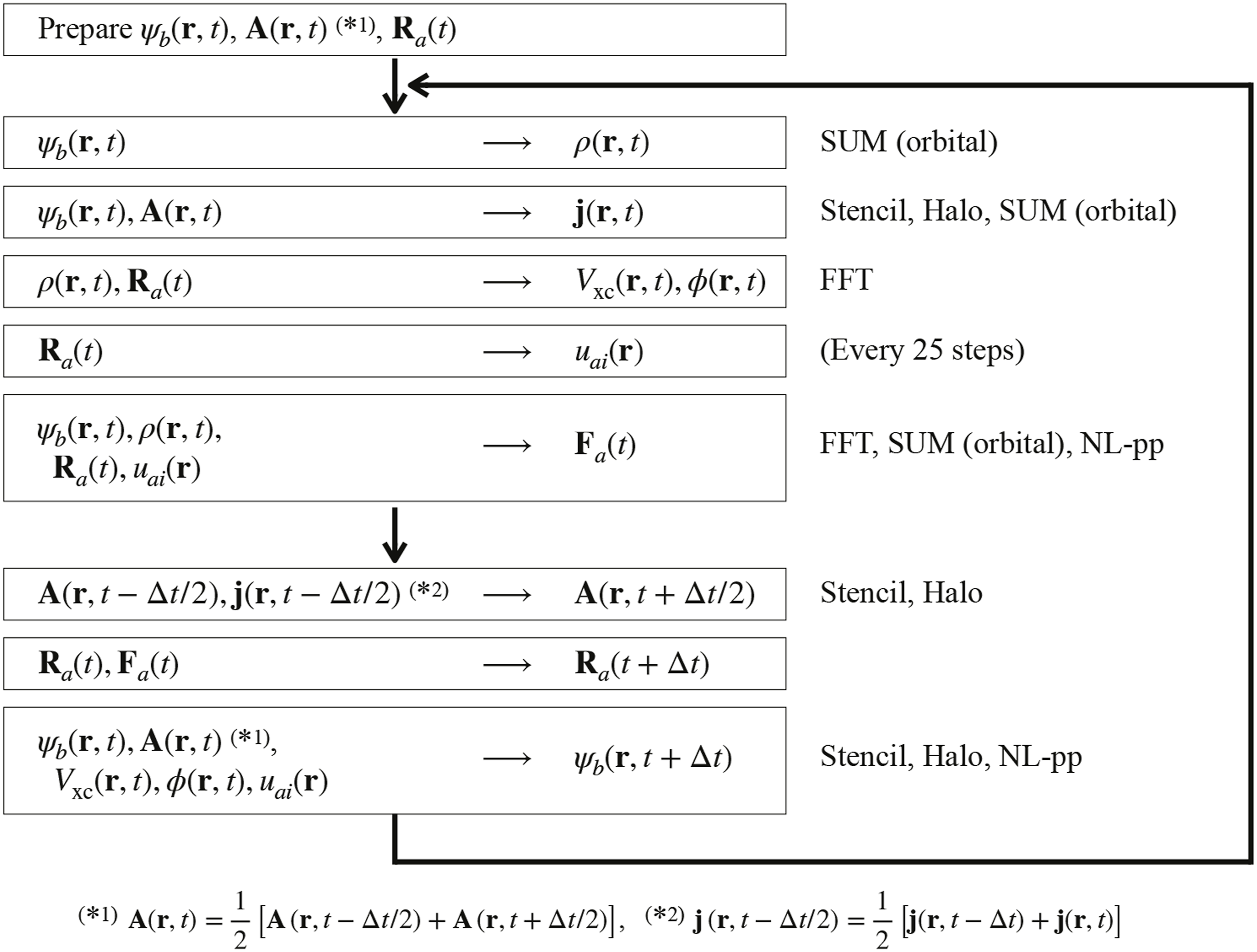
We solve the equations within a rectangular box area using a 3D Cartesian grid for coordinate
We first prepare an initial state in which the electron orbitals ψ
b
are set to the ground state solution of static DFT. The vector potential
When the electron orbitals ψ
b
, vector potential
From the density ρ(
After preparing these quantities, we update the electron orbitals ψ
b
. We use an explicit solver, Taylor expansion method 9-point stencil diagram is shown.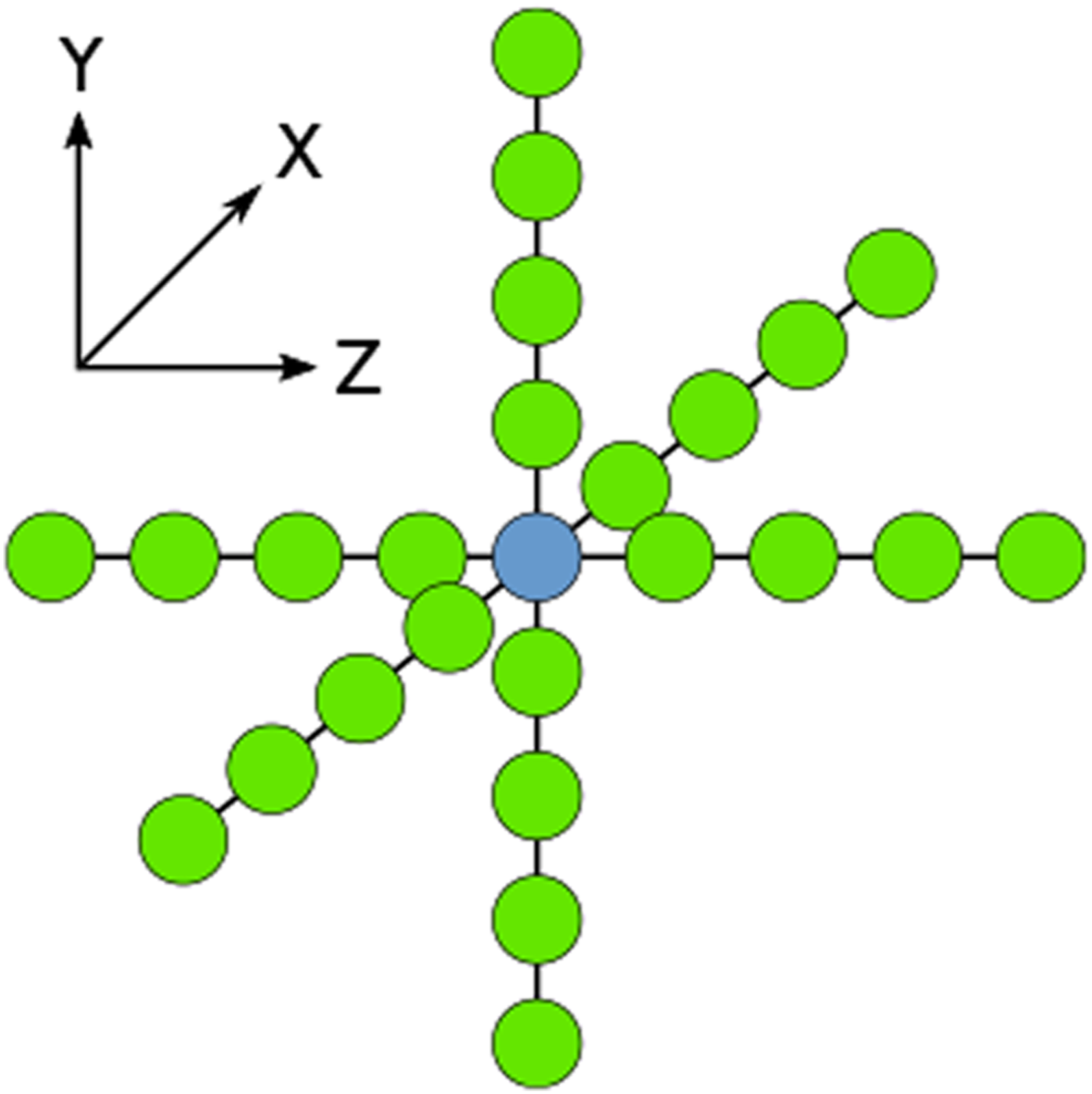
The second calculation is the operation of the nonlocal PP that includes the projector functions u
ai
(
The number of grid points included in the projector, which we denote
With a shift of a half time step, the vector potentials and ionic coordinates are updated. To update the vector potential, we use an explicit scheme with a time step much smaller than the update of the electron orbitals, Δt
EM
≃Δt/100
This also involves stencil calculations and halo communications.
2.2. Parallelization and communications
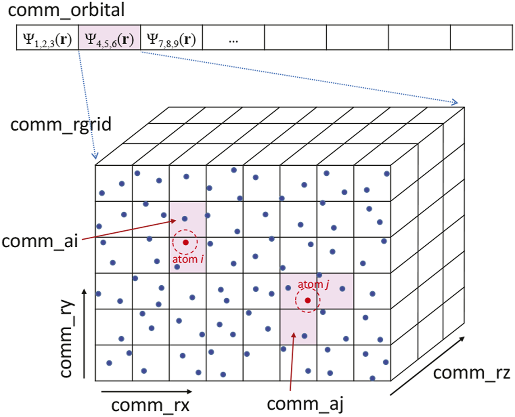
We introduce process division, as illustrated in Figure 3. We assume that the entire system can be divided into Pall processes with Pall = PorbitalP
rx
P
ry
P
rz
. We first divide the entire system into Porbital processes. This is used to divide the orbital index b = 1⋯Norbital of ψ
b
and also divide the atomic index, a = 1⋯Natom. For each divided system, we introduce a division of P
rx
, P
ry
, and P
rz
to divide the 3D Cartesian grids of L
x
, L
y
, and L
z
. Later, we also use Prgrid = P
rx
P
ry
P
rz
. The process allocation and communicators of electron orbitals ψ
b
(
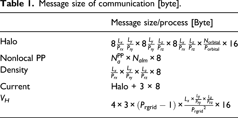
Message size of communication [byte].
Stencil calculations appear in the Hamiltonian operation, calculations of the vector potential, and the electric current density. For stencil calculations, halo communications must be performed. Because a periodic boundary condition is imposed, each MPI process achieves peer-to-peer communication in six directions in the halo communication. Calculations of the electron density and electric current density involve the convolution calculation of ψ b . To sum all electron orbitals, Allreduce is used.
To update the Hartree potential, a Poisson equation is solved using FFT. FFTE version 6.0 is used in SALMON and utilizes six-step FFT; therefore, all-to-all communications appear to transpose matrices (Takahashi, 2000). Because the electron density is a function of only the spatial coordinates, parallelization of the FFTE for the scalar potential calculations can be performed by all MPI processes. However, because the cost of all-to-all communications in the FFTE may be substantial as the number of processes increases, we perform the calculation redundantly using the processes of Prgrid. A condition for the division of MPI processes and conditions for the use of FFTE are as follows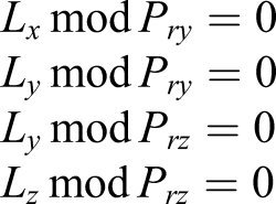
2.3. Optimization of stencil calculation
There are two means of optimizing the stencil calculation. One is to improve single-instruction multiple-data (SIMD) optimization of the compiler, while the other is to perform hand-coding of SIMD without relying on the compiler. We performed two types of optimizations and compared the results. We implemented hand-coding in the C programming language using Arm C Language Extension for SVE (ACLE) intrinsics (Arm Developer, 2010).
Single-instruction multiple-data optimization using the Fujitsu compiler was improved as follows. Figure 4 presents the Fortran code for stencil calculation for improving SIMD optimization in the Fujitsu compiler. In general, it is preferable to include all finite difference calculations in a single loop for the efficient use of cache and register memories. However, the Fujitsu compiler has software pipelining optimization that treats and optimizes calculations using pipeline dividing register memories. To utilize the function, register memory used in the loop should be sufficiently small to achieve latency hiding. Therefore, calculations within a loop body should be as small as possible to make full use of software pipelining. Pseudo FORTRAN code of stencil computation for optimizing Fujitsu compiler.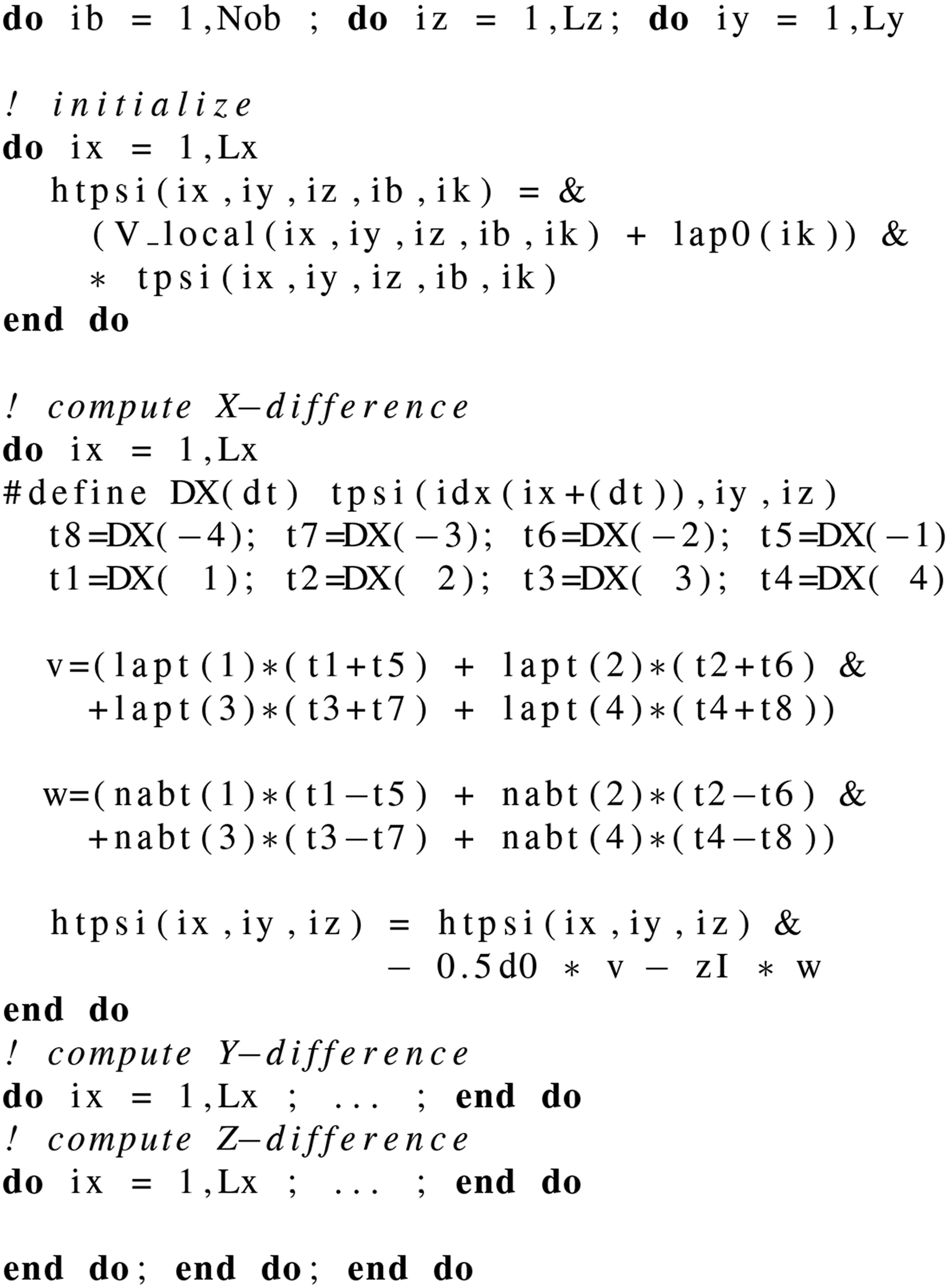
Because the stencil calculation in SALMON has a deep halo of four grid points in each direction, the loop body is long, and software pipelining could not be applied. Therefore, the loop in the x-axis, which uses memories that allocate continuously, was divided into four parts so that software pipelining was possible in each loop. In Figure 4, the loop length that the software pipelining was enabled was set to more than 24–48. This fact conforms to the grid sizes that were used.
We next consider the hand-coding vectorization using ACLE. In Hirokawa et al. (2018), we discussed optimization of the same calculation using Intel AVX-512 intrinsics. In SVE (Scalable Vector Extension) instructions that A64FX supports, it is possible to set the hardware SIMD length between 128-bit and 2048- bit. It is expected that high performance can be obtained without hard efforts of hand-coding vectorization by setting the hardware SIMD length of A64FX to 512-bit, the same as AVX-512, and by transforming AVX-512 implementation to 512-bit SVE. However, it turned out that the expected performance was not obtained because the software pipelining could not be optimized.
In our stencil calculation, each orbital is treated independently. We note that an efficient implementation of the stencil calculation was reported by treating multiple states at once that works to achieve efficient SIMD vectorization and cache utilization (Andrade and Aspuru-Guzik, 2013; Andrade et al., 2015).
3. Simulation of light–matter interaction
3.1. Physical system
In the present performance evaluation, we calculated a system of a thin film of amorphous SiO2. The dangling bonds at the surface were terminated by H atoms. For weak scaling measurements, we selected a system of
MPI Process mapping of weak scaling evaluation.
MPI Process mapping of strong scaling evaluation.
3.2. A representative simulation
To show that the present simulation method is applicable to light–matter interaction that appears in frontiers of optical science, we performed a calculation of light–matter interaction in a thin-film glass composed of 10,224 atoms using 27,648 nodes. Figure 5(a) illustrates the atomic configurations. Spatial grids of 216 × 288 × 480 were prepared in a box area of 3.95 nm × 5.13 nm × 8.65 nm. A thin film was extended in the x and y directions with a periodic boundary condition. In the z direction, the 6.6-nm-thick SiO2 thin film was sandwiched between two vacuum areas of approximately 1 nm above and below the film. A linearly polarized pulsed light irradiated normally on the surface. The pulsed light was characterized by an average frequency of 3.1 eV, pulse duration of 10 fs, and pulse intensity of 1014 W/cm2. (a) Atomic configuration and box area adopted in the representative simulation. (b) Electron density in the ground state around the upper surface. (c) Electron density change during irradiation of the laser pulse.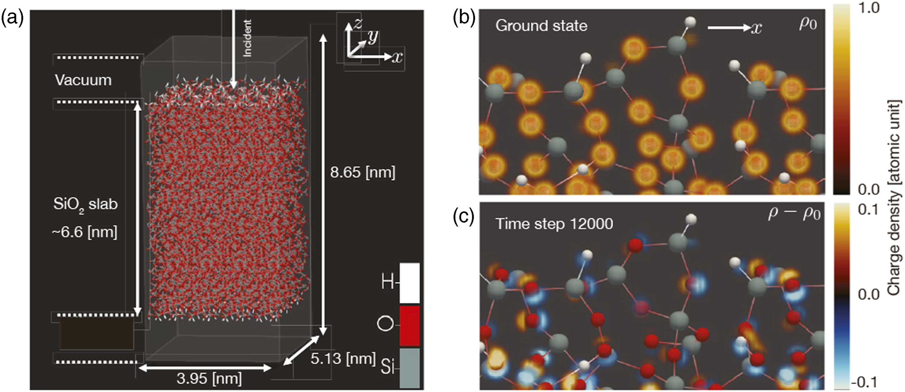
To begin the calculation, it was necessary to prepare the ground state of the system. Instead of calculating the ground state solution of the entire system of 10,224 atoms, we solved a smaller system composed of 852 atoms that has the same thickness in the z-direction. Solving the smaller system with 4 × 3k-points, four for x-direction and three for y-direction, we can prepare the initial orbitals of the entire system of 10,224 atoms by unfolding the Bloch orbitals of 852 atoms with k-indices. We then provided random velocities for all ions to thermalize the system.
Pulsed light irradiates in the negative z direction, and the electric field of the incident pulse induces electronic excitations in the medium. The transferred energy eventually moves to thermal ionic motion. There also appears a reflected wave in the negative z direction and a transmitted wave in the positive z direction. These complex dynamics were described simultaneously in the present simulation.
A time step of 0.000 75 fs was selected, and a time evolution of 8000 steps was performed as a single job. Approximately 3 hours of wall-clock time were required. We performed three connected jobs. The first job was performed without a laser pulse to thermalize the system. The following two jobs were performed with the pulsed light. In total, a simulation of 18 fs was successfully performed. Although we did not impose orthonormalization of the electron orbitals during the time propagation, the norm was conserved in good accuracy. The total number of electrons that is given as twice of the sum of the norms of the electron orbitals is conserved within 0.3 out of 53,280, indicating the accuracy of 5 × 10⁻⁶ level.
To illustrate the dynamics, Figure 6(a) shows electric field of the incident pulsed light and that of the reflected pulse as functions of time. In Figure 6(b), the electronic excitation energy that represents the energy transfer from the light pulse to the medium by a nonlinear multiphoton process is displayed as a function of time. In Figure 6(c), spectral intensity of the reflected wave is shown. It shows a clear high harmonic generation signal, a typical signal reflecting the nonlinear optical response. Excitation processes on the atomic scale are visualized in the right panels of Figure 5. Figure 5(b) illustrates the electron density distribution in the ground state, expanding the surface region of the thin film. Reflecting the oxide nature of SiO2, the electrons are mostly localized around oxygen atoms. Figure 5(c) displays the difference in the electron density from the ground state during laser irradiation. Here, the dipole oscillations of electron clouds around oxygen atoms are observed as a dominant feature. (a) Electric field of incident laser pulse adopted in the representative simulation (red) and that of reflected pulse (blue). (b) Calculated energy transfer from laser pulse to electrons. (c) Spectral intensity of the reflected pulse.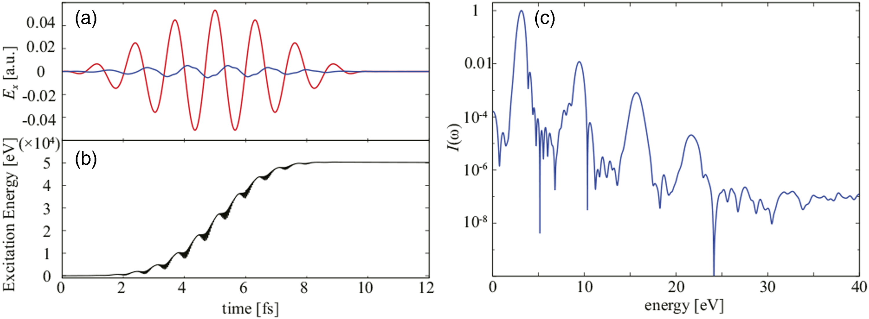
4. Performance results
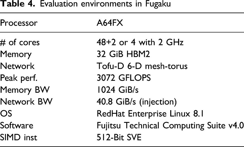
4.1. Evaluation environment
Evaluation environments in Fugaku
Variables of MPI process distribution.
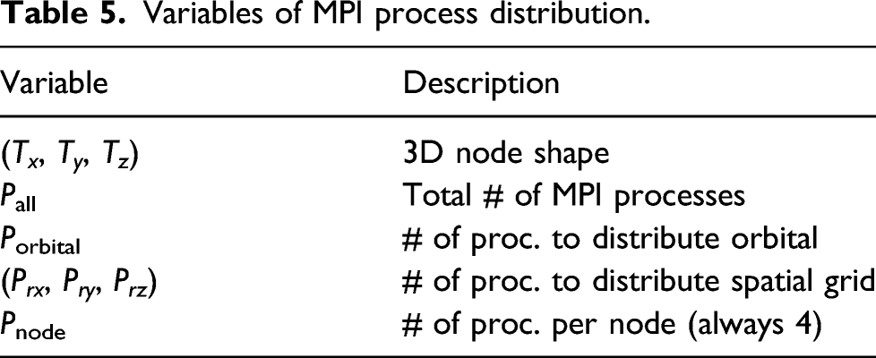
In Fugaku, we allocated four processes per node for the efficient use of the CMG. It is desirable to allocate it to the continuous P rx processes. Therefore, we performed 4D process mapping by dividing each 3D process space of (T x × Pnode, T y , T z ) into the subprocess space of (P rx , P ry , P rz ). The number of subprocess spaces in each 3D process space was equal to Porbital.
To achieve the allocation in practice, we first expressed Porbital as the product of three integers: Porbital = P
ox
P
oy
P
oz
. These were selected so that the following relations were fulfilled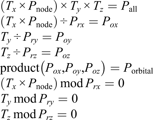
By identifying (P ox , P oy , P oz ) that satisfy these conditions, 4D process mapping can be realized by placing it in the subprocess space.
An example of process mapping is presented in Figure 7. Here, the process number is set as follows Schematic diagram of MPI process mapping to 3D network system is shown. Each circled number indicates a node. Solid lines indicate communications related to spatial grid, and dashed lines indicate communications related to orbitals. See text for details.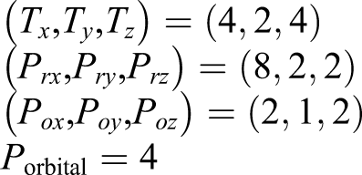
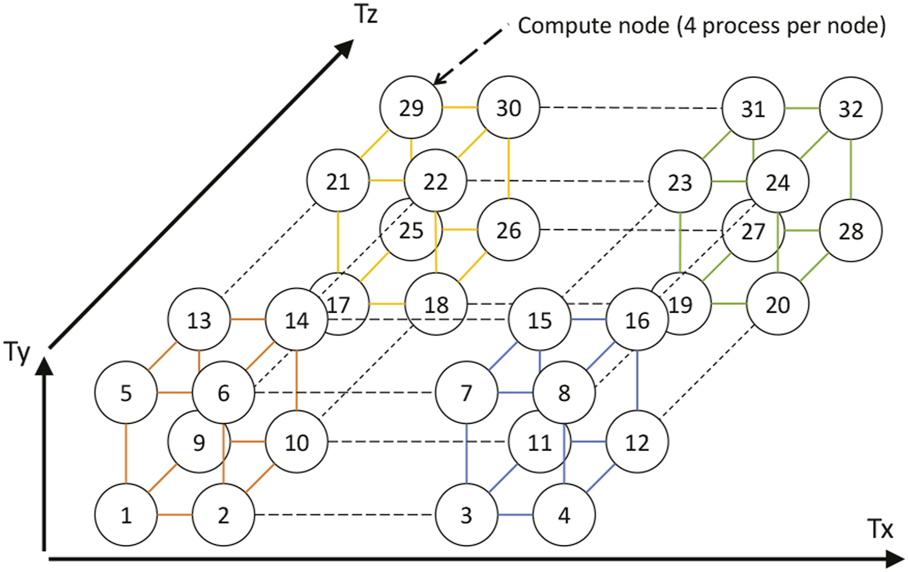
Let us consider Node 6 and examine its communications. Communications related to the spatial grid are confined and localized within a block composed of nodes (1, 2, 5, 6, 9, 10, 13, 14). However, communications related to the orbitals arise between nodes (6, 8, 22, 24) that belong to different blocks. Because collective communications dominate between electron orbitals, it is desirable for the shape of (T x × Pnode, T y , T z ) to be close to a cube so that the hop count can be minimized. However, the actual shape of the nodes that can be realized is restricted by the system construction.
In the present real-time TDDFT calculation, we used the above setting optimizing the communication performance between spatially distributed processes. The setting would be different for ground state DFT calculations in which communications among electron orbitals dominate, such as in Gram-Schmidt orthogonalization and subspace diagonalization. For those cases, the hop count in Porbital should be minimized, while communications between the spatial grid processes would become negligible. This can be realized by exchanging P rx and Porbital in the above construction: communications within Porbital can be confined within nodes (5, 6).
4.2. Single-node performance
The performance of the stencil calculation using A64FX is presented in Figure 8. The problem size was set to 1283 spatial grids, and measurements were performed using 48 OpenMP threads. In this figure, “Auto” indicates SIMD optimization by the compiler, “Hand” indicates hand-coding SIMD instructions using 512-bit SVE instructions of A64FX, and “SWP” indicates that optimization by software pipelining is effective. Mini-benchmark results of the stencil computation (A64FX).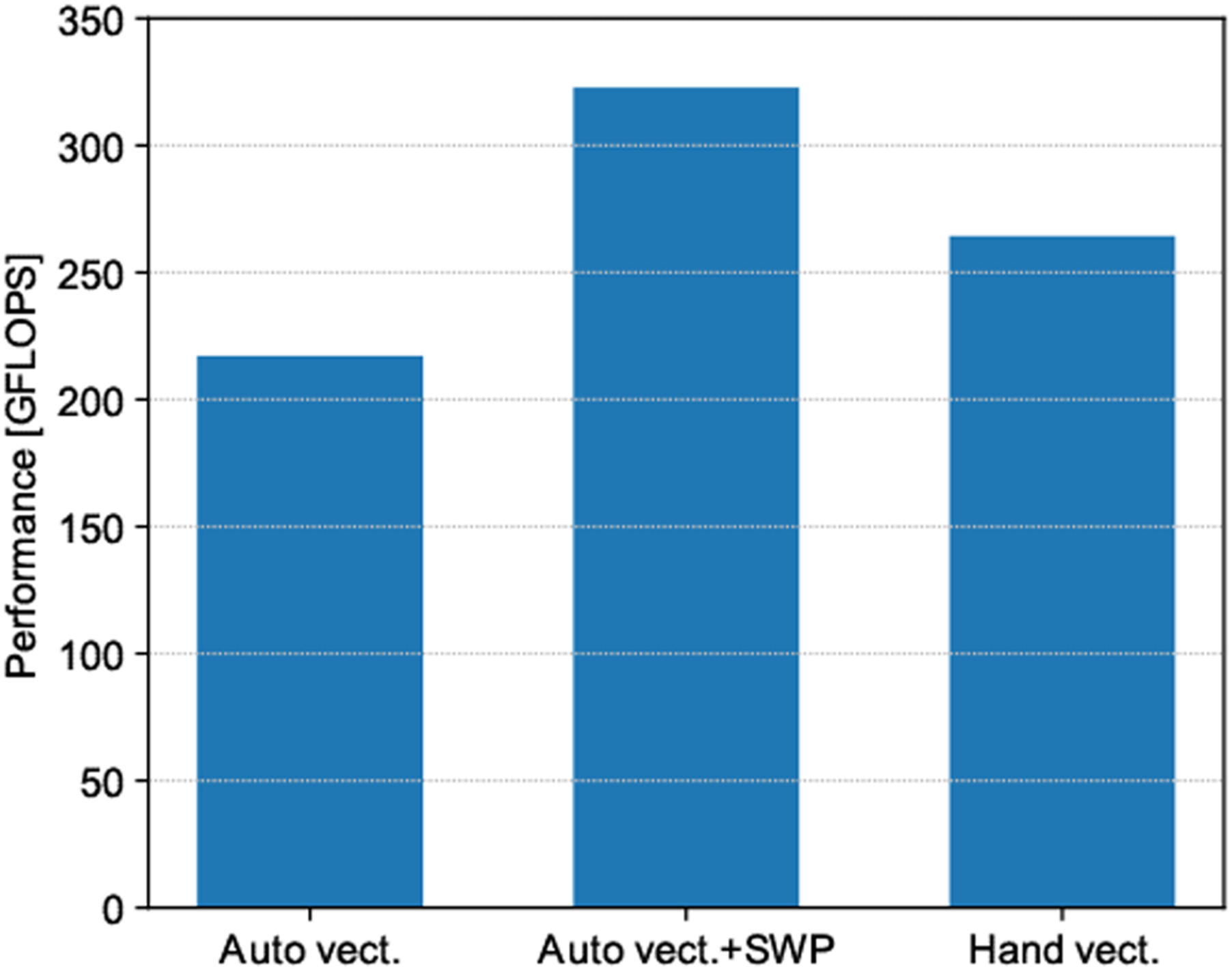
By combining optimization methods to strengthen the compiler, such as software pipelining with SIMD optimization, it may not be necessary to rewrite the code at the intrinsic level. In the present hand-coding optimization, the loop structure became too complex for the Fujitsu compiler to analyze, and it was not possible to activate software pipelining. By performing hand-coding for the operation corresponding to software pipelining, it may have been possible to further increase the performance. However, the code with SIMD intrinsics led the compiler to fail other optimizations; therefore, performance evaluation was not achieved.
The analysis in Figure 8 reveals that the maximum performance was 322.72 GFLOPS, and the Byte/FLOP value was approximately 2.68. From these numbers, the achieved memory bandwidth is estimated to be 866 GiB/s. Because the memory bandwidth of A64FX is 1024 GiB/s, our code achieved highly efficient memory bandwidth of 84.5%. Figure 9 presents the achievable peak performance and achieved performance using the Roofline model (Williams et al., 2009) with the memory bandwidth of the L2 cache and HBM2. Because stencil calculations are ultimately bounded by the memory bandwidth of HBM2, we believe that we obtained performance that was very close to the maximum possible value in A64FX. However, it should be noted that the Byte/FLOP was estimated without considering the effect of cache memory. Therefore, the true achievable peak performance likely lies between the two Rooflines of L2 cache and HBM2. Therefore, further optimization is necessary. Achievable peak/achieved performance of stencil computation.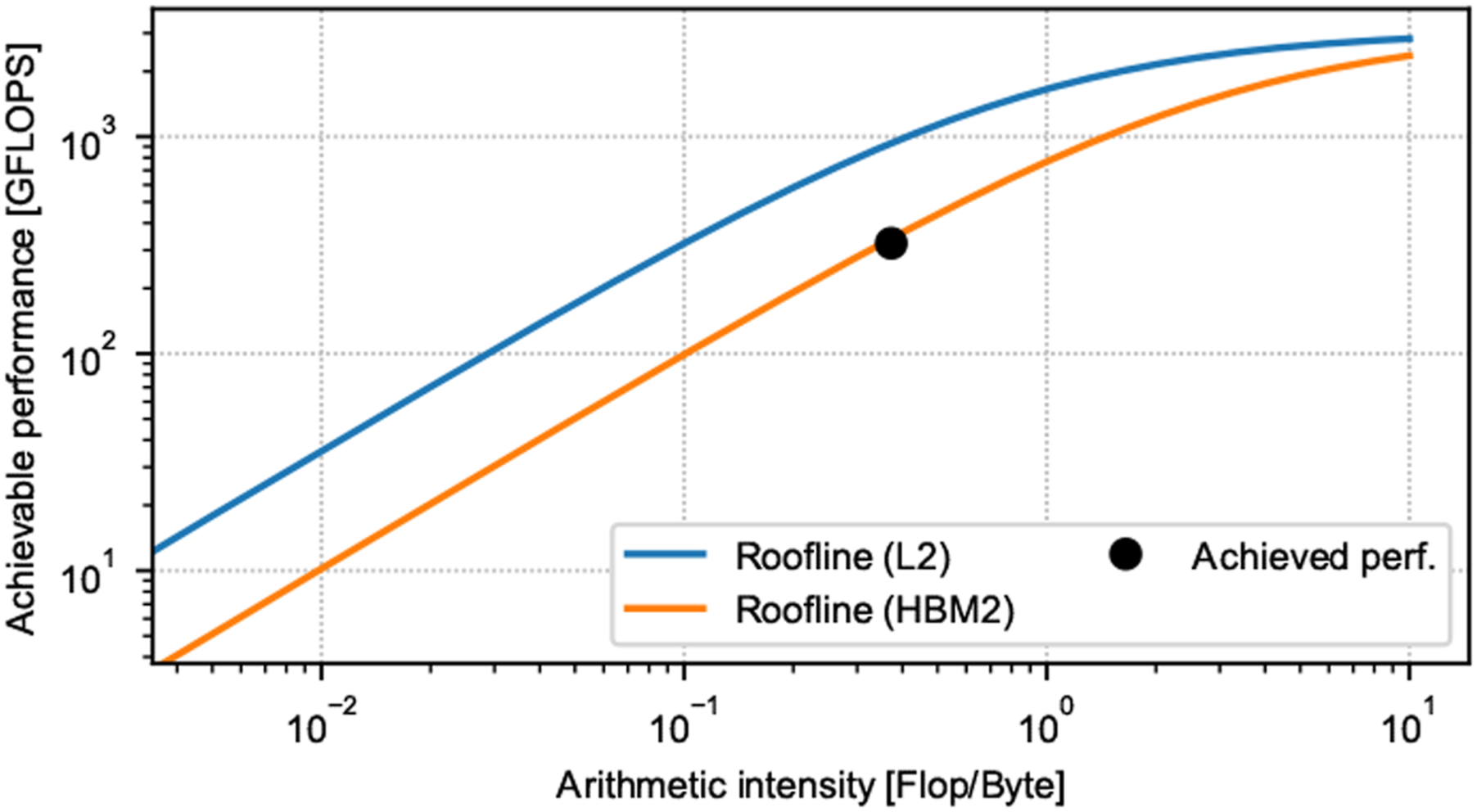
The single-node performance was measured for a slightly different system: Au54 nanoparticle on Si thin film, with Lx,y,z = (128, 64, 81) and Norbital = 648. The performance was measured using the performance profiler provided by Fujitsu. The profiling was performed in four MPI processes with one MPI process per CMG, and the FLOPS of each CMG were measured. The measured performance revealed almost the same value for the four CMGs, and the total performance was 321.66 GFLOPS. In comparison with the peak performance of Fugaku, the effective performance was approximately 10.5%. We believe that this is a reasonable performance that is close to the maximum that can be expected in view of the Byte/FLOP bound.
We conclude that the performance of calculations in SALMON is apparently bounded by the memory bandwidth. The Byte/FLOP value of A64FX is estimated by 1024 GiB/s ÷ 3072 GFLOPS ≃ 0.33. Because the maximum possible Byte/FLOP value is 0.33 ÷ 2.68 = 12.3%, we anticipate that the maximum achievable performance is also bounded by this value. The effective performance of 10.5% that was observed in this examination is close to the maximum achievable value of 12.3%.
4.3. Weak/strong scalability
Figure 10 displays the computational time per one time step. Updating of the projector u
ai
( Weak scaling results up to 27,648 compute nodes.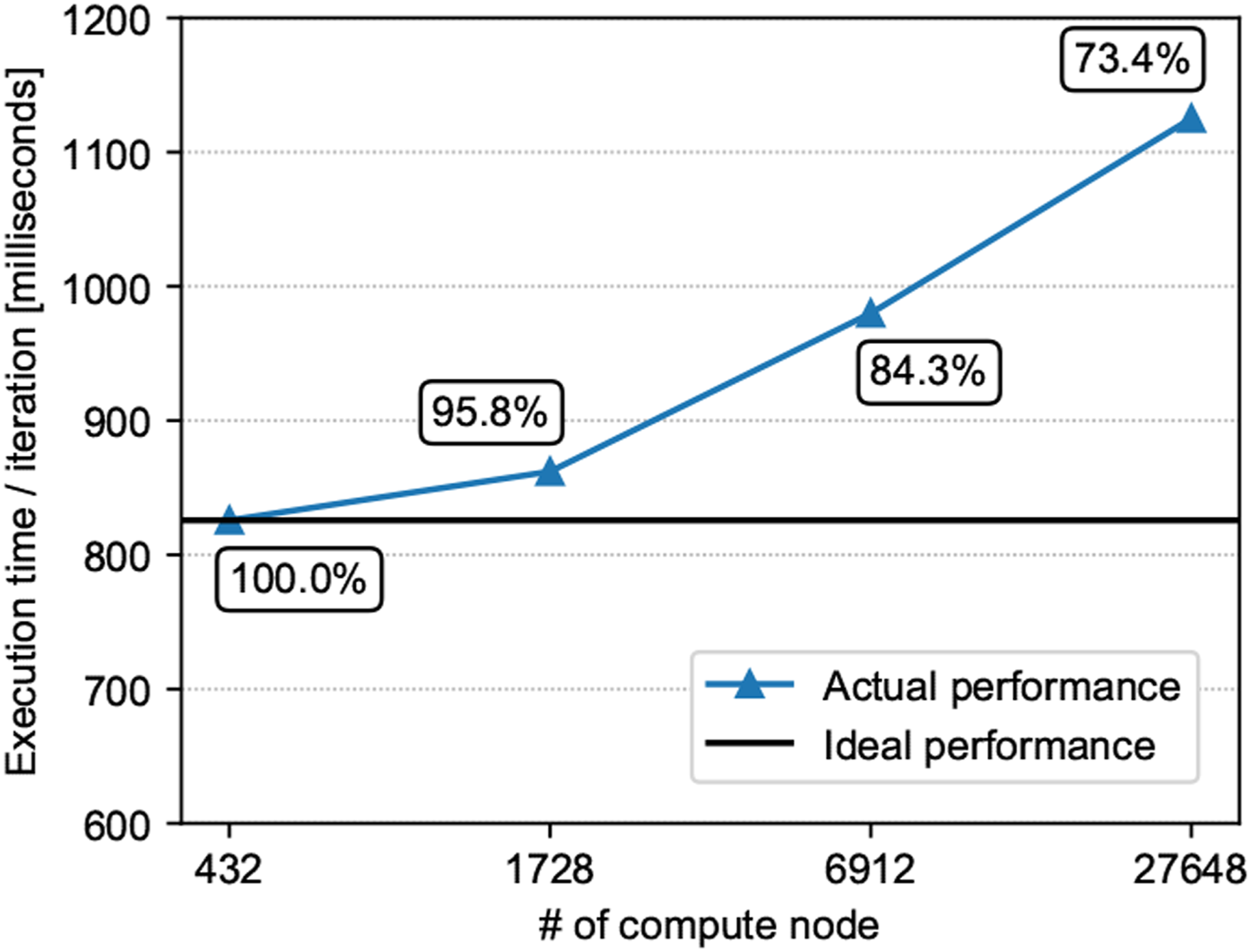
Figure 11 presents a bar chart displaying the decomposition of the calculations and communications, where half-width bars indicate the time of communications. The maximum elapsed time among processes is used in the plot. Approximately half of the total computation time was spent on the operation of the Hamiltonian on electron orbitals that scaled as O(N2). The communication cost constituted approximately 60–70%. The next dominant was the FFT calculation of the Hartree (scalar) potential. The result of the FFT was also used to calculate the force. Many other calculations were not negligible, including calculations of the electron density, electric current density, and force. Updating the projectors u
ai
( Breakdown of weak scaling results.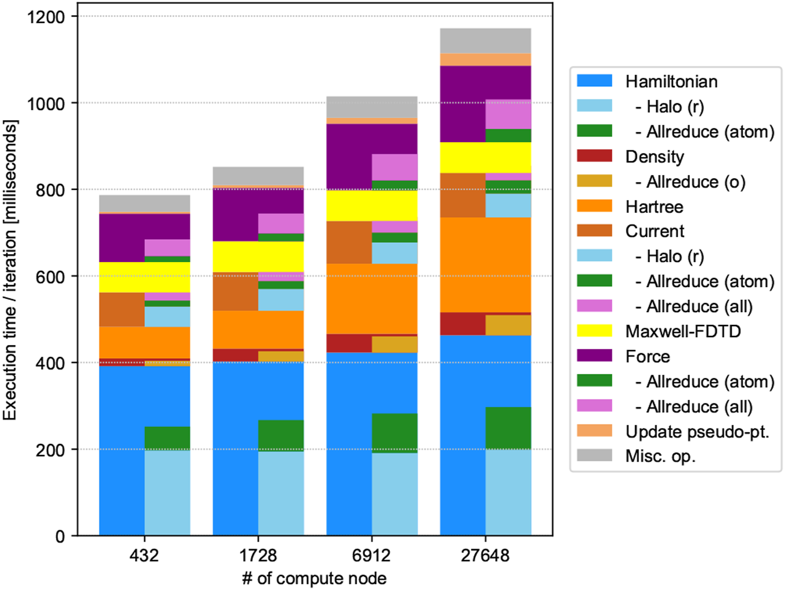
We used FFTE to perform the FFT calculation. For the (x, y, z) 3D FFT calculation, FFTE adopts (y, z) two-dimensional (2D) block parallelization. We simply assigned comm_ry and comm_rz communicators to perform the FFT calculations. MPI_Allreduce communications appeared in the communicators of comm_rx to collect information in the x direction that was not parallelized. Because the number of grid points in the x direction increased from 1728 nodes to 6912 nodes, the execution time of the Hartree calculation increased by a factor of approximately 2. Fixing the number of grid points in the x direction would prevent this problem from occurring.
Due to competition between the complex parallelization in SALMON and the process mapping, it was difficult to prevent the deterioration of the efficiency of the FFTE calculation. Because the grid number in the z direction was fixed in the current setting of the physical system, it is reasonable to assume that the performance would have increased if we performed FFTE using (x, y) 2D blocks. However, this was unsuccessful. The reason is that the increase in MPI_Allgether was greater than the decrease in the MPI_Alltoall cost. It is also important to note that communications in P rz were always between different nodes, while communications in P rx were primarily within one node.
Figure 12 presents a bar chart for the strong scaling measurement. Horizontal black dotted lines indicate the expected performance that was determined if calculations of the 70% part affected by the spatial division scaled completely. Examining the decomposition, the communication costs increased relative to the calculation. This was due to the increase in halo communications between different nodes, as we increased the number of processes in the z and y directions, as illustrated in Table 3. Because the parallel efficiency was 79–82% as a whole, we consider that strong scalability was superior to weak scalability. Breakdown of strong scaling results up to 27,648 compute nodes.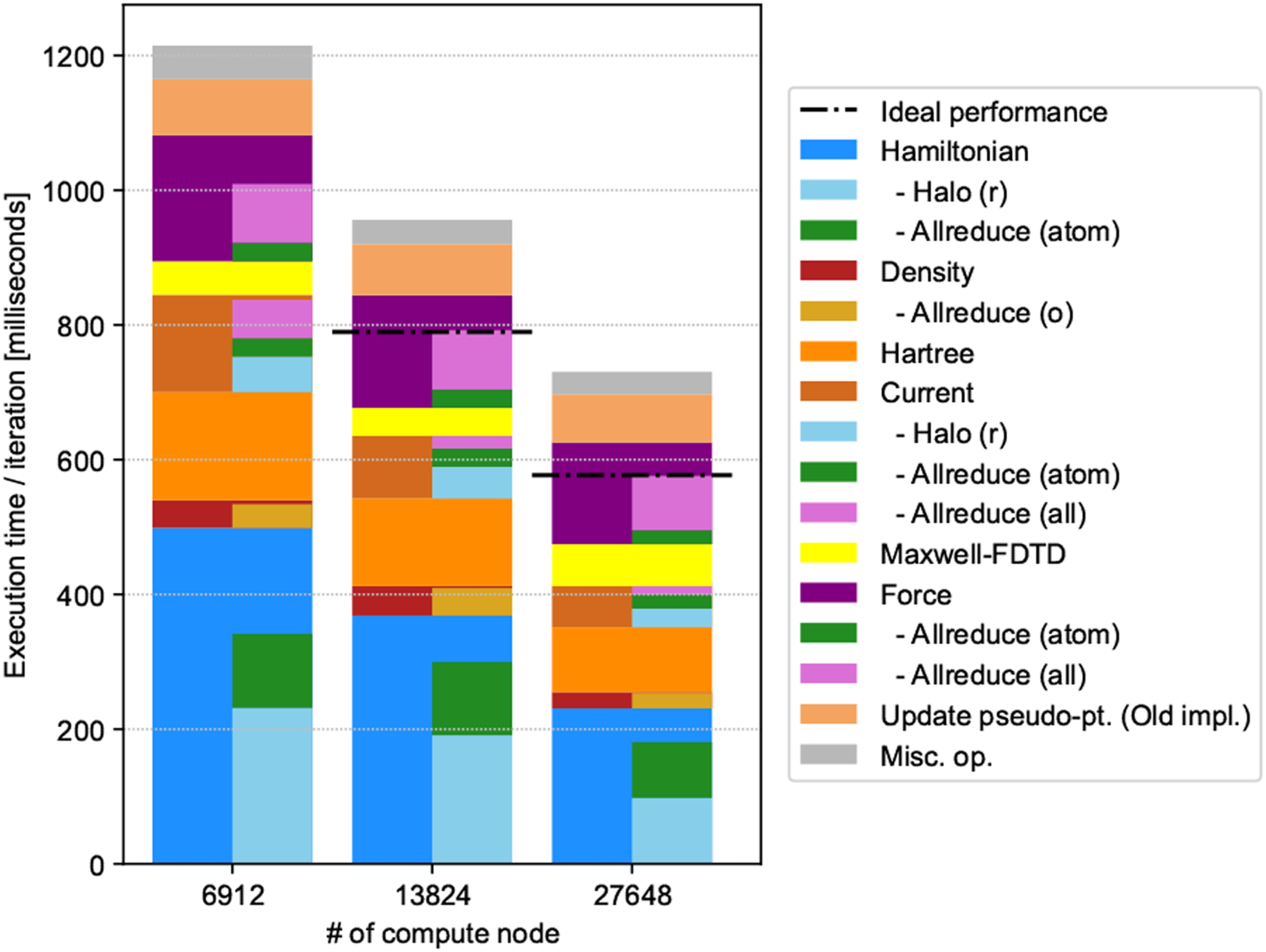
4.4. Effective performance and time-to-solution
PFLOPS performance in weak scaling evaluation.
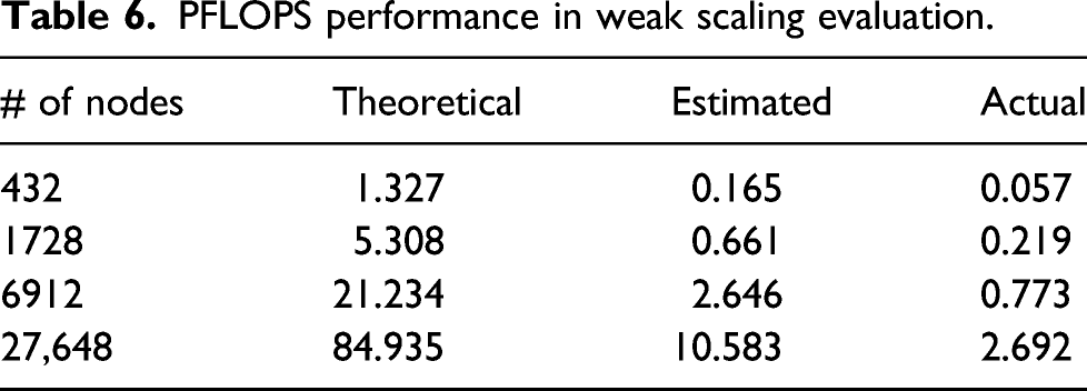
Although this value does not look very high, we consider that the present calculation succeeded to achieve a very high performance in view of the time-to-solution. As described in the Introduction, the measurement of a similar real-time TDDFT calculation was performed for a bulk Aluminum of 5400 atoms (59,400 electrons) using a full system of Sequoia Blue Gene/Q (Draeger et al., 2016). To our knowledge, this is the largest real-time TDDFT calculation so far. It was reported that it took 53.2 s for a calculation of single time step. The effective performance was reported to be as high as 43%. In our present measurement, we achieved a calculation of single time step of the system composed of 13,632 atoms (71,040 electrons) by less than 1.2 s. In view of the theoretical performance, 84.935 PFLOPS of the present measurement using a part of Fugaku and more than 20 PFLOPS of Sequoia, the time-to-solution of the present calculation is more than 10 times superior to the previous result.
The difference of the peak performance between two calculations originates from the adopted basis function. In Draeger et al. (2016), a plane-wave basis was adopted. The bottleneck was the operation of the nonlocal PP that is treated as dense-matrix operations and was accelerated by BLAS dgemm and zgemm. In our 3D grid representation, operations of the Hamiltonian are performed using sparse matrices. Our strategy was to minimize the number of FLOP, although it harms the nominal value of the effective performance.
4.5. Performance of the representative simulation
Figure 13 presents a bar chart of the computation time of the representative production run with the same breakdown as for weak/strong scaling. In the representative simulation, we adopted eight operations of the Hamiltonian on the orbitals to achieve a better conservation of the norm, while we adopted four operations in the weak/strong performance measurements. As a result, the time of the Hamiltonian operation appears larger in the present decomposition. We also note that the elapsed time was smaller than for weak scaling using 27,648 nodes. This was due to the system size; we performed the representative simulation for a system composed of 10,224 atoms. Breakdown of representative production run with 27,648 compute nodes.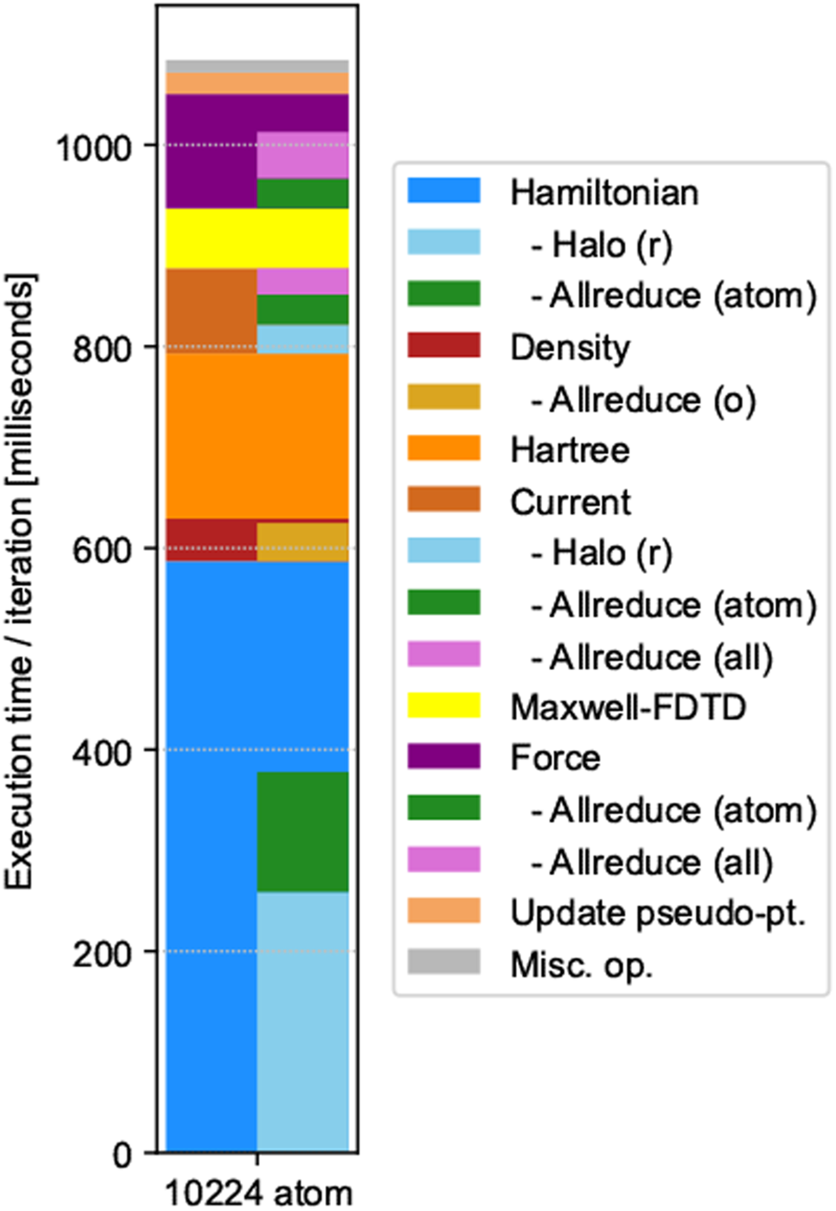
The breakdown of the representative simulation does not include the elapsed time of file I/O. There are two types of file I/O: reading the ground state solution to prepare the initial state, and outputting the calculated results for analysis and visualization.
The file I/O time to read the initial state was approximately 200–1200 s. The time to write the data for restart/checkpoint was approximately 150 s. Because we performed the time evolution calculation of 8000 steps as a single job that costs approximately 9000 s, the file I/O time related to input/restart did not constitute a significant portion of the total elapsed time.
With respect to the I/O related to the analysis of the results, the electric field, induced electric current, and the ionic coordinates, velocities, and forces were outputted every 70 iterations. The electron density ρ(
5. Summary and outlook
We have developed a novel ab initio simulation method for light–matter interaction that can be applicable to simulate forefront experiments in optical science. In the method, coupled equations are solved simultaneously: electromagnetism analysis for light electromagnetic fields, ab initio TDDFT for electron dynamics, and molecular dynamics for ionic motion. Electron orbitals as well as scalar and vector potentials are discretized on 3D Cartesian grid. The code is efficiently parallelized by dividing the spatial grid, electron orbitals, and ionic indices.
We carried out a thorough optimization of the code on the Fujitsu A64FX processor. As a test simulation, we have carried out a simulation of amorphous SiO2 thin film composed of more than 10,000 atoms using 27,648 nodes of the Fugaku supercomputer. It has been shown that the code shows an excellent time-to-solution satisfying 1 second per step that is required in practical applications.
In the present report, we discuss light–matter interaction calculations of a thin film material of a thickness of several nm. While it is important to model not only film materials but a prototype of bulk surfaces, the interaction of pulsed light with nanomaterials of various 3D structures, either isolated or placed on surfaces, will also be extremely interesting. There are a variety of phenomena in nano-optics and nanophotonics that can be tackled by large-scale calculations using SALMON.
One limitation that should be addressed is the scalability of FFT calculations. For calculations of infinitely periodic systems, the use of FFT is unavoidable. However, the elapsed time of FFTE displayed the largest increase in weak scalability, as illustrated in Figure 10. In the current code, the z axis was assigned a special role: the material was periodic in the xy plane while the pulsed light propagated along the z axis. FFTE adopts parallelization in yz that assigns a special role to the x direction: MPI_Allgather communication is required along the x direction. We plan to improve the performance of FFT by lifting this restriction of the directional setting in our code.
Another important means of reducing communication costs is the use of process mapping to the Tofu-D network. In the current stage using 27,648 nodes, only a 12 × 48 × 48 shape was allowed. With the entire Fugaku system, we expect greater flexibility in parallelization so that improved performance can be achieved. To this end, we must be aware that (1) process division should be determined to fit the Tofu shape and (2) the grid and process numbers should satisfy the requirements of the FFTE.
Footnotes
Acknowledgements
The authors would like to express their deepest appreciation to late Prof. Katsuyuki Nobusada for his momentous contribution in the early stage of this project.
Declaration of conflicting interests
The author(s) declared no potential conflicts of interest with respect to the research, authorship, and/or publication of this article.
Funding
The author(s) disclosed receipt of the following financial support for the research, authorship, and/or publication of this article: This research was supported by MEXT as a priority issue theme 7 to be tackled by using Post-K Computer, by JST-CREST under Grant No. JP-MJCR16N5, and by MEXT Quantum Leap Flagship Program (MEXT Q-LEAP) Grant Number JPMXS0118068681.
Author biographies
Yuta Hirokawa was a researcher at the Center for Computational Sciences, University of Tsukuba, Japan. Currently, he is an HPC evangelist in Prometech Software, Inc. He received a PhD in Engineering in 2018 from University of Tsukuba, Japan. His research interests are high-performance computing, especially code tuning and performance optimization.
Atsushi Yamada is a senior researcher at the Center for Computational Sciences, University of Tsukuba, Japan. He received a PhD degree in physics in 2003 from Nagoya University. His research interests are computational physics and chemistry, molecular science, condensed matter physics, biophysics, and optical science.
Shunsuke Yamada is a researcher at the Center for Computational Sciences, University of Tsukuba. He received Master and PhD degrees in physics from the University of Tokyo in 2014 and 2017, respectively. His research interests include first-principles calculations for light–matter interaction and condensed matter physics.
Masashi Noda was a researcher at the Center for Computational Sciences, University of Tsukuba. Before that, he received a Master of Engineering in 2004 and a PhD in 2007 and worked at the Institute for Molecular Science for 11 years. Currently, he is an office worker at Academeia and supports people engaging in research and development.
Mitsuharu Uemoto is an assistant professor at the Department of Electrical and Electronic Engineering, Kobe University. He received a master degree from Osaka University in 2011 and a PhD degree in 2014. His research interests include first-principles calculation of the nonlinear optical properties in the nanoscale materials.
Taisuke Boku is a professor and currently the director of Center for Computational Sciences, University of Tsukuba. He received master and PhD degrees from Faculty of Science and Technology, Keio University. He is a specialist on high-performance computing systems and has been collaborating with various fields of domain scientists for coding and optimization on scientific applications. He is a coauthor of ACM Gordon Bell Prize in 2011.
Kazuhiro Yabana is a professor at the Center for Computational Sciences, University of Tsukuba. He obtained his PhD in 1987 in physics from Kyoto University. He was appointed assistant professor at Niigata University in 1988, moved to University of Tsukuba in 1999, and is in the current position since 2004. His research interests include computational materials science, computational optical sciences, and theoretical nuclear physics.