
Abstract
In recent years, development and progress in modern packaging resulting from degradable natural resources have grown remarkably. In this study, chitosan–polyaniline film was prepared with a combination of different concentrations of polyaniline and various synthesis times to produce antimicrobial and biodegradable packaging film. The physical, electrical, and mechanical properties of the films were investigated. The interaction between chitosan and polyaniline was confirmed by Fourier-transform infrared spectroscopy (FTIR) and X-ray diffraction patterns. The size and morphology of the synthesized particles were examined by scanning electron microscopy. The results indicated that the synthesized polyaniline particles had a spherical shape (45–100 nm). The antimicrobial and antifungal activity of the films against Aspergillus niger fungi (antifungal area: 61.47 mm2) and Escherichia coli bacteria (antimicrobial area: 187.27 mm2) increased with increasing the concentration of polyaniline. The results obtained from the study of the effect of polyaniline on the electrical conductivity of the chitosan film showed that increasing the polyaniline concentration and synthesis time resulted in decreased electrical resistance of the film, for which the film with the highest aniline concentration and the highest synthesize time had the lowest resistance. According to the mechanical property results, tensile strength (TS) and elastic modulus were increased due to the addition of the polyaniline to the polymer matrix. The chitosan blank film had a lower TS than nanocomposites. As the final results, the chitosan–polyaniline film has good electrical conductivity, indicating that the produced film could be used in intelligent food packaging.
Introduction
Due to the increased production and consumption of petroleum polymers and plastics in the daily life of humans, the diseases caused by food poisoning have become a major threat to human health and the environment and have contributed to the emergence of the packaging industry. Since the bulk of the packaging industry is made up of plastics, the packaging industry can be linked to petroleum products. Therefore, the increasing growth of population, pollution caused by packaging materials derived from oil derivatives, and problems caused by various methods of disposal of these contaminations, including burning, burial, and recycling, have attracted more attention toward biopolymers and biopackaging. Biodegradable films and coatings are good alternatives to synthetic films in the packaging industry due to their eco-friendliness and low dependence on nonrenewable resources and, therefore, have attracted the attention of many researchers. Synthetic plastics that are used to pack different types of foods are causing serious environmental problems. The environmental impacts of plastic consumption in the food industry have encouraged the packaging industry to produce packaging out of renewable materials. Biodegradable packaging protects food products against mechanical, physical, and chemical damage and prevents their quality loss. It can also prevent microbial activity as an antimicrobial carrier in the form of antimicrobial packaging and increase the shelf life of food products. In recent years, many studies have been carried out to replace synthetic polymers with biodegradable biopolymers, especially for food packaging. Most disadvantages and problems with synthetic polymers are not raised for biopolymers due to their biodegradable nature, and this has made many researchers in the food packaging industry study the use of a variety of biopolymers to make biodegradable packaging.
1
Nanotechnology is one of the most important and the fastest growing parts of advanced technology. Products containing nanoparticles can be used in various industrial, medical, personal, and military applications. Nanocomposite is a compound substance with at least one of its phases having nanoscale dimensions (between 1 nm and 100 nm).
2
Nanocomposites are new alternatives to traditional methods of improving the properties of polymers. Nanocomposites are currently being used for the packaging of nonalcoholic beverages and foodstuffs because of their thermal properties, improved resistance, and conductivity.
3
Chitosan is a linear polysaccharide composed of
Polyaniline is one of the oldest synthetic conductive polymers with high electrical conductivity. Basically, polyaniline is known as a redox polymer and is prepared by chemical and electrochemical methods in an acidic environment, which depends on the type of its application. If thin films, better properties, and purity are required, then electrochemical method is recommended. Polyaniline is used in various fields, including microelectronics, corrosion coatings, and sensors because of its diverse structure, thermal and radiant stability, low cost, easy synthesis, and conductivity. Its application in the preparation of static electricity, eliminating layers, and corrosion-resistant coatings can be referred to as the most common use of this polymer. Converting conducting polymers into films and fibers will pave the way for the widespread use of this polymer. 8 Its application in preventing corrosion has created a revolution in metal protection. 9 Its excellent protection against static electrical charges has led to its application in manufacturing high-quality electronics components. The absorption and transfer of heavy metals from aqueous solutions and reduction of environmental pollution are also some of its recent applications. 10 Polyaniline composites with polymers include polyester, nylon, polyvinyl chloride, and so on. By utilizing the mechanical properties of classical polymer (insulator) as a matrix, electrical properties and redox polyaniline can open a new world in expanding the scope of polyaniline applications. 11
In this study, new conducting antibacterial chitosan–polyaniline film was provided by chemical polymerization and studied its mechanical, antibacterial, and electrical characteristics. In fact, the provided film has antibacterial properties and electrical conductivity that can be used in food packaging as a smart film.
Materials and methods
Chemicals and equipments
The following chemicals were used: chitosan (medium molecular weight, DD 99%, Mark, India), glycerol of 98% purity (Merck, Germany), acetic acid 1% (Merck), distilled water, aniline (Sigma-Aldrich, USA), ethanol (Merck), concentrated hydrochloric acid (Merck), agar nutrient culture medium (Sigma), and Potato Dextrose Agar (PDA) culture medium (Mir Media, Italy).
Equipments: RADVAG digital scale with an accuracy of 0.001, model WTB 200, PECO sterile heater, Iran; UV-VIS Spectrophotometer, model UNICO 2100 (UNICO-US), Glassware (Bécher, Erlenmeyer flask, pipette, thermometer, etc.) Sina Glass, Iran; multipurpose X-ray diffraction (XRD; MPD) Model B.V (made in The Netherlands); HIOKI multimeter machine, model DT4252, XRD device (MPD) model (Philips, Xpert), made in The Netherlands; electronic scanning microscope, Tescan Vega-3 incubator (Shimax, Iran); and spectrometer (Fourier-transform infrared spectroscopy (FTIR)) model 2002, Germany.
Synthesis of chitosan film
First, 5 g of chitosan powder (DD, 99, Mark) was dissolved in 300 mL solution of acetic acid (vol/vol 1%). Then, to improve the flexibility of the film, 2 mg of glycerol (Merck with 98% of purity) was added to the solution as a plasticizer, and then, the solution was stirred at 90°C for 8 h, and after complete uniformity, 150 mL of the solution was added to plastic molds (20 × 30 cm2) and placed at ambient temperature for 72 h to dry (Figure 1(a)).

(a) Chitosan film and (b) chitosan–polyaniline composite films.
Preparation of chitosan–polyaniline film
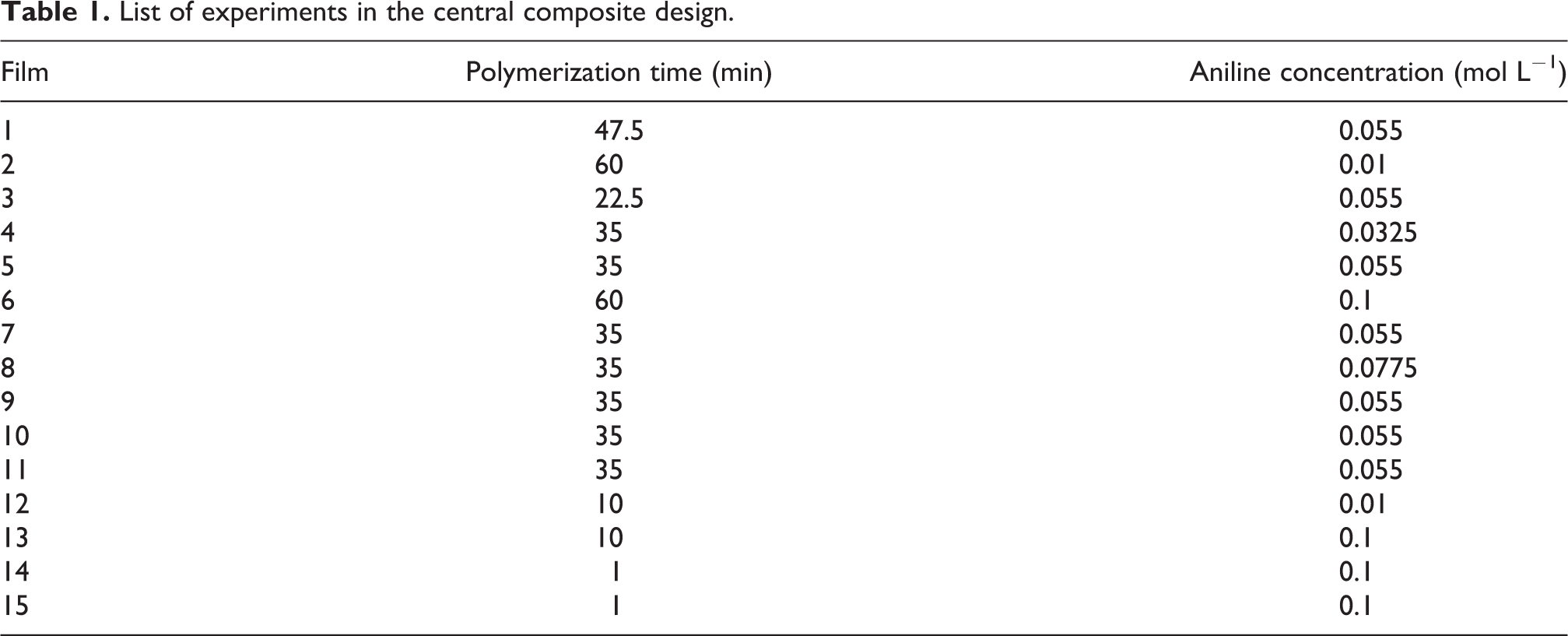
At first, 500 mg of potassium dichromate was dissolved in 15 mL of distilled water and then, 35 mL of ethanol was added to it. To acidify the medium, 2.5 mL of hydrogen chloride (37%) was added to the above solution and then, aniline was added to the solution (the volume of aniline was based on experimental design according to Table 1), Then, a chitosan film (5 × 5 cm2) (prepared in the previous step) was placed in a solution. The polymerization period was done according to the experimental design in Table 1. This procedure was repeated for all samples. Figure 1(b) shows the different chitosan modification-polyaniline composite films.
List of experiments in the central composite design.
X-Ray diffraction analysis
The XRD test was carried out on the films by MPD (Philips model, made in The Netherlands) located in the X-ray lab of Tarbiat Modarres University. At first, the samples were compressed onto disks. The nickel-filtered copper K α ray with a wavelength of 0.145 nm was produced. To do the test, the X-ray producing generator was set at 40 kV and 40 mA, and the samples were exposed to X-rays. Refractive radiations from the sample were measured at ambient temperature and at an angle 2θ ranging from 2° to 70°. Crystallite size was measured via the Scherrer formula.

where λ is the wavelength of X-ray (0.154 nm), β is the peak width of diffraction in half of the height of the sample, and θ is the angle of reflection.
FTIR spectroscopy
To carry out the FTIR test, Perkin Elmer instrument (USA) was used at Urmia University. Thin tablets with the thickness of less than 1 mm were obtained for 10 min in a tablet machine through mixing water and milling samples of the film or nanoparticles coated with dry bromide potassium to the ratio of 1:20 and by applying a pressure of about 60 kPa. Transmission spectrum of the samples was analyzed in the wavelength range of 400–4000 cm−1 and with a resolution of 0.5 cm−1.
Scanning electron microscopy
The microstructure of the produced films was investigated using a Tescan Vegan3 scanning electron microscopy (SEM) in the Razi Metallurgical Institute (Tehran). To investigate the effect of the addition of polyaniline on the microstructure of the produced films, electron microscopic images were prepared from the film surface. First, the films were adhered to the aluminum base by silver glue. The bases are dried up in a coating/disperser device to the critical point and were covered with gold for 5 min. Imaging of the specimens was carried out using a SEM with an applied force of 20 kW and a magnification of 6 μm. 12
Measuring the electric resistance of films
Conductivity or electrical resistivity of films was measured by HIOKI multimeter model DT4252. First, the device was set on the resistive meter and two electrodes of the device were placed on the film 1 cm apart from each other. Then, the electrical resistance value was recorded. Electrical resistance was measured at five points on the back and front of the films and the average was calculated.
Measuring antimicrobial properties of the film
The antimicrobial properties of the film were measured using a diffusion method at the agar level. The antimicrobial properties of the film were measured in a solid culture medium in Aspergillus niger and Escherichia coli bacteria at the Nutrient Agar (NA) and PDA levels. At first, the culture medium was prepared for each bacterium, the solution containing the bacteria was added to the medium, and pieces of the film were cut as large as 6 mL and were put in the plates. Then, the plates were placed in an incubator for 72 h at 37°C, so that the bacteria could grow completely. After the end of growth, the mean diameter of the created halo was measured with a caliper and the area of the generated halo was calculated. 13
Measurement of the mechanical properties of the films
Tensile tests were performed using TA.XT Plus, stable microsystems, UK, and standard brush (ASTM D882) at the Faculty of Agriculture, Urmia University. Three mechanical films were selected for optimum performance and a blank film. For this purpose, films in the 5 × 1 cm2 dimensions were cut with a special film cutter. The distance between the jaws was 5 cm, and the jaw speed was 0.83 mm s−1. The maximum failure factors (in terms of newton) of the gradient were expressed per second and the distance to the breaking point (millimeter) by the device, and the strain coefficients of the breakdown (STB) and the tensile strength (TS) were determined by the following relations. In this regard, TS in MPa, force in terms of newton, and thickness (D) and film width (W) in meters 14 :


Statistical analysis
In this work, statistical analysis was done in two stages: in stage 1, central composite design (at 95% probability level) was used for studying aniline concentration (in five levels) and polymerization time (in five levels) effects on the chitosan–polyaniline film electrical resistance (Table 1). In stage 2, to study aniline concentration (0.01 and 0.1 mol L−1) and polymerization time (10 and 60 min), a factorial design with three replications was used. In stage 1, statistical analysis was carried out based on a central composite design at the 95% probability level and using statistical software of Design expert-7, and in stage 2, Minitab (Version 17) software was used for data analysis; Tukey’s test was used to compare the means. Also, significant levels of data were considered at the 5% probability level (p < 0.05). Meanwhile, the data in tables and forms were considered as a mean ± standard deviation (SD).
Results and discussion
XRD study
Figure 2 displays the results of XRD analysis for pure chitosan film (a), polyaniline (b), and chitosan–polyaniline nanocomposite (c). The XRD pattern of chitosan film in Figure 2(a) exhibits the weak peaks at diffraction angle 2θ = 11.7° and sharp peaks at 2θ = 21° that indicate the high degree of crystallinity morphology of chitosan. 15 Figure 2(b) and (c) depicts the XRD patterns of the polyaniline and chitosan–polyaniline. The XRD patterns of polyaniline (Figure 2(b)) exhibit three peaks at 2θ = 18°, 2θ = 21.7°, and 2θ = 26°, which indicates that the polyaniline has semicrystalline characteristic. 16 However, the chitosan–polyaniline (Figure 2(c)) XRD pattern shows a decrease in the relative intensities of the peaks. When the peaks of polyaniline are compared with chitosan–polyaniline, it is observed that the peaks at 2θ = 18°, 2θ = 21.7°, and 2θ = 26° have become broader. This decrease in intensity of the peaks in chitosan–polyaniline can be associated with a disorder in the planes of polyaniline, suggesting the formation of new chemical bonds between chitosan and polyaniline. 17,18 In other words, the penetration of polyaniline particles into the chitosan film matrix and its uniform distribution throughout the matrix will reduce the chitosan crystalline mode. According to Bragg’s law, the lower the diffraction angle is, the better the nanoparticle diffusion has occurred in the polymer matrix. The results are consistent with the findings of other researchers. 19,20

XRD spectrum patterns of (a) chitosan, (b) polyaniline, and (c) chitosan–polyaniline.
FTIR study
FTIR spectroscopy is a technique to examine the status of the bonds and microstructure of the materials. In other words, it is used to study hydrogen bonds and other reactions as well as the ability to blend polymers. 21 Figure 3 displays the FTIR spectrum of polyaniline (Fig. 3(a)), chitosan (Fig. 3(b)), chitosan–polyaniline (Fig. 3(c)). Figure 3(a) shows the FTIR spectrum for polyaniline. The peak formed at a frequency of 845 cm−1 represents the N–H flexural bonds of the functional groups participating in hydrogen bonds. The presence of benzoid bonds at a frequency of 1520 cm−1 and kinoid vibrations at a frequency of 1590 cm−1 indicates that polyaniline is used in the form of emeraldine salt. The presence of the peak at a frequency of 3400 cm−1 represents the symmetric and asymmetric tensile bonds of the N–H aromatic ring in polyaniline. 22,23 Figure 3(b) shows the FTIR spectrum for pure chitosan. Pure chitosan has distinct absorption peaks at a frequency of 3442 cm−1 due to symmetric and asymmetric –NH2 tensile vibrations and –NH2 bending bonds at a frequency of 1557 cm−1. The peak appearing at a frequency of 2850 cm−1 is related to the C–H tensile bond (central carbon–hydrogen bonding) in the chitosan film, which could be considered a reason for the high relative strength of these films. 16,24 The peak at a frequency of 1200 cm−1 is due to the asymmetric stretch of C–O–C and the peak at a frequency of 1600 cm−1 is due to symmetric and asymmetric C–O tensile vibrations indicating sucrose structure for chitosan. 25,26 Figure 3(c) shows the FTIR spectrum for chitosan–polyaniline indicating the formation of the bond between chitosan and polyaniline and also the hydrogen bonding of active OH groups between chitosan and polyaniline at a frequency of 2900 and 3429 cm−1. 26,27 The peak intensity reduction occurs at a frequency of 2800 cm−1 for chitosan–polyaniline nanocomposite in comparison with pure chitosan, so that some peaks disappear. These results indicate the reaction between chitosan and polyaniline and the formation of a chemical bond between chitosan and polyaniline, which proves the composite formation. 28 The results are consistent with the findings of other researchers. 28,29
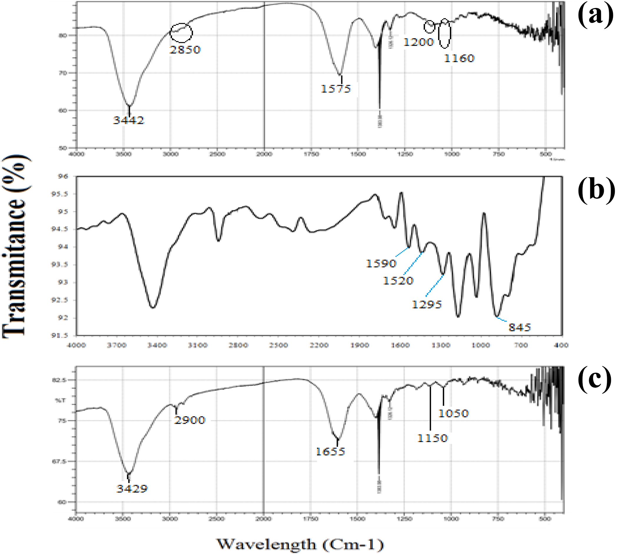
FTIR spectrum patterns of the (a) polyaniline, (b) chitosan, and (c) chitosan–polyaniline.
SEM study
Homogeneity of the composite, the presence of the cavity, the level of dispersion of nanoparticles in the matrix, and nanoparticles orientation can be detected via SEM. Morphology of chitosan film and chitosan–polyaniline nanocomposite film was studied by SEM technique. Figure 4(a) shows the SEM image of pure chitosan film, and Figure 4(b) shows the SEM image of chitosan film modified with polyaniline particles (0.1 M at 60 min). The SEM image of pure chitosan film showed that the film was smooth without pores, which indicated the homogeneity of the prepared film. The chitosan–polyaniline SEM image showed that the polyaniline particles were synthesized uniformly and the particle shapes were almost spherical and in nanodimensions (45–100 nm). Although some aggregations were observed, it should be noted that the particles were dispersed in the chitosan matrix in a nonuniform manner. The results are consistent with the findings of other researchers. 12,30

SEM image of (a) pure chitosan film and (b) chitosan film modified with polyaniline (0.1 M, 60 min).
Measuring electrical resistance of the films
Figure 5 shows the effect of synthesis time and aniline concentration of polyaniline on conductivity or electrical resistance. As the synthesis time and the concentration of monomer of polyaniline increase, electrical resistance decreases and electrical conductivity increases. The reason for this is that polyaniline is conductive and by increasing the time, more nanopolymers are synthesized on the film leading to the decrease of electrical resistance and increase of electrical conductivity. Furthermore, as the aniline concentration increases, due to conductivity, electrical resistance decreases. The results show that the produced films have a high capacity for use in smart food packaging. It should be mentioned that the SD for each film electrical resistance was below 8%. In addition, the electrical resistance of films is a very important factor that can be used in biosensors and gas sensors, and so on. The results are consistent with the findings of other researchers. 31

Three-dimensional plot of film electrical resistance against the synthesis time (A: A) and aniline concentration (B: B).
Antifungal and antibacterial property
The results of antifungal property on A. niger fungus are reported in Table 2. The antifungal activity of the control film and the optimal films on A. niger are shown in Figure 6(a). With regard to the antifungal and antibacterial nature of chitosan, all of the four selected films showed a nongrowth halo, so that the largest halo is seen in F6, which has both high synthesis time and more nanopolymers, and the smallest nongrowth halo is related to F2, which has the lowest aniline concentration. The results indicate that the synthesis time has little effect on the antifungal properties of nanocomposites compared to the aniline concentration, so that the film with a high aniline concentration and high synthesis time had the highest nongrowth halo and the film with low aniline concentration showed the lowest nongrowth halo on the Aspergillus fungus. The results of the antimicrobial properties of the control film and optimal films on E. coli bacteria are reported in Table 2. Figure 6(b) illustrates antimicrobial property of the control film and optimal films against E. coli. The control film (pure chitosan) and F3 showed nongrowth halo against E. coli bacteria. The results indicate that the aniline concentration, in comparison to the synthesis time, has the greater effect on antimicrobial properties of films, so that the highest antibacterial effect is on the film with high aniline concentration, and the lowest antibacterial effect is on the film with low aniline concentration. According to the results, the higher aniline concentration results in the production of the greater amount of synthesized polymer and therefore increases electrical conductivity. According to the results, increasing the amount of synthesized polymer increases the antibacterial property of films, so it can be concluded that the film that has less electrical resistance (more electrical conductivity) has a better antibacterial effect. There are different reported research studies that discussed the reasons for antimicrobial properties of chitosan–nanoparticle films. 32,33
Comparison of average (±SD) of antimicrobial activity of chitosan–polyaniline film against Aspergillus niger fungi and Escherichia coli bacteria.a

aData are means of three replicates. Means with different letters within a column indicate significant differences (p < 0.05).

Effect of chitosan–polyaniline film on the growth of (a) Aspergillus niger and (b) Escherichia coli.
Mechanical properties of the films
The results of the evaluation of mechanical properties are depicted in Table 3. As can be seen, TS and elastic modulus are increased due to the addition of the polyaniline to the polymer matrix. Figure 7(a) shows the TS of the film samples chitosan. The blank sample has a lower TS than nanocomposites. The highest TS and elastic modulus are for F2, F6, and F13, respectively. This could be due to the uniform dispersion of polyaniline nanoparticles in the chitosan polymer matrix, a strong interaction between chitosan and polyaniline by an ion bond that creates new and strong bonds between chitosan and polyaniline. Figure 7(b) shows the STB of the film samples. According to the results, blank sample has the highest strain at the fracture point relative to the optimal specimens and is flexible and has less TS. The other results indicate improved mechanical properties and increased TS of biopolymer films due to the addition of nanoparticles. 34,35
Comparison of average (±SD) of mechanical features of the films.a
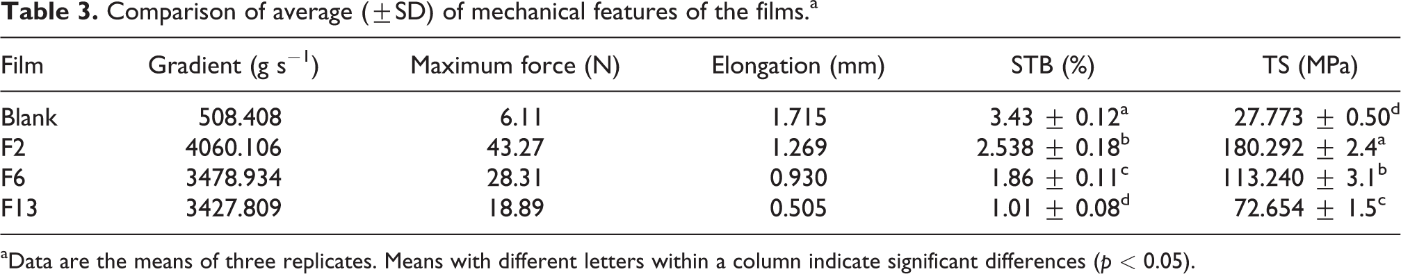
aData are the means of three replicates. Means with different letters within a column indicate significant differences (p < 0.05).
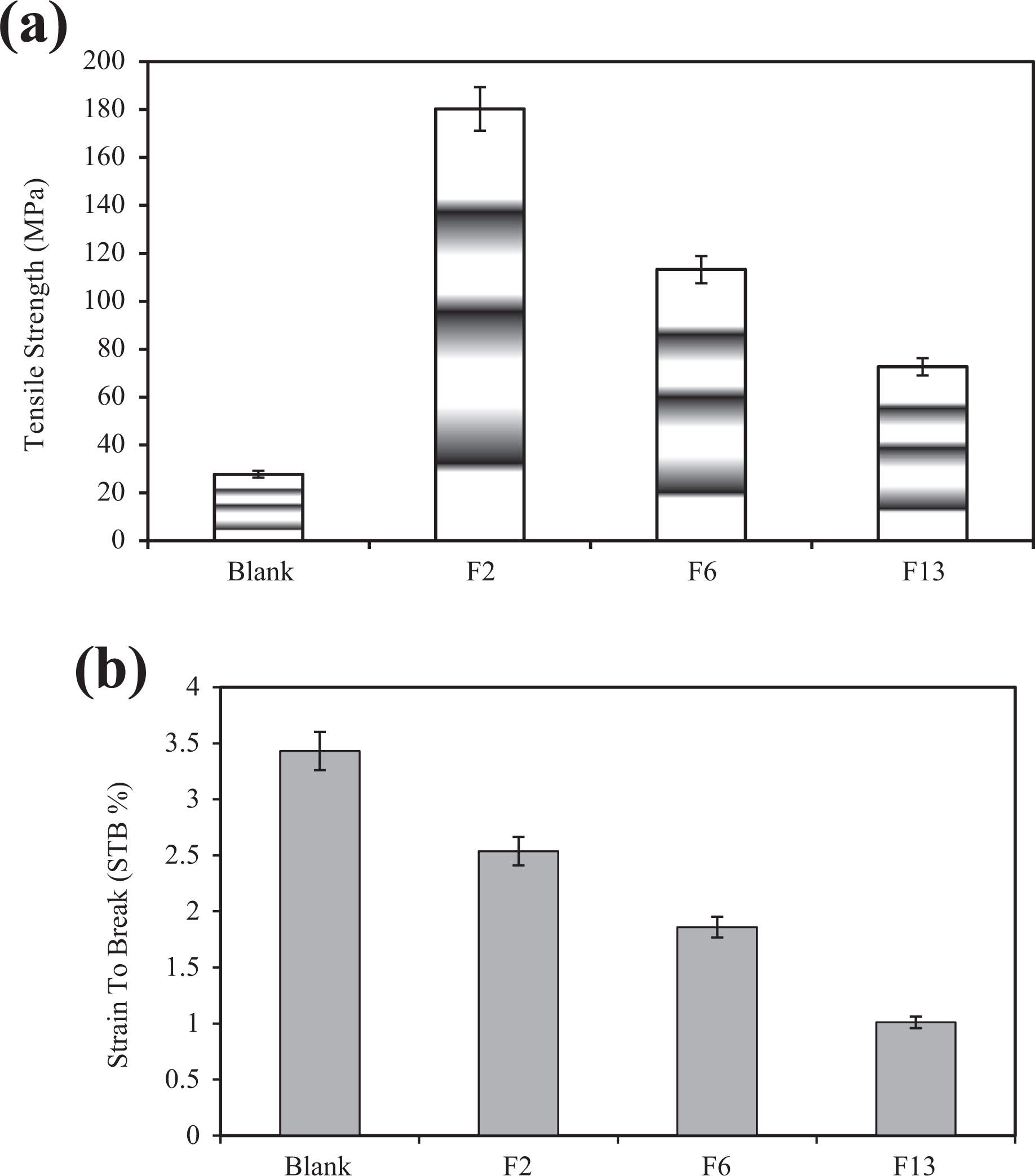
(a) Strain-to-break and (b) the tensile strength of films.
In the end, it should be mentioned that the presented work reports a new biodegradable/antifungal/antimicrobial conducting film based on chitosan that as a novel film has the ability to be used as an active film in food packaging. In addition, due to the fact that the produced film has electrical conductivity and its electrical conductivity can be changed in different conditions, so the film can also report the storage conditions of food products.
Conclusion
The biodegradable/antifungal–antibacterial/conducting film based on chitosan–polyaniline was prepared by chemical polymerization method. The crystallinity, morphology, chemical structure, conductivity, and mechanical properties of prepared films were studied by different techniques. The nanostructure of polyaniline and the interaction between chitosan and polyaniline was confirmed by XRD, SEM, and FTIR pattern. According to the results, the addition of different aniline concentration to the chitosan film improved the antimicrobial, electrical, and mechanical properties of chitosan film. The antimicrobial properties of nanocomposites were satisfactory and showed that the film had a high potential for antibacterial packaging. The study of mechanical property results showed that the addition of polyaniline improves the mechanical properties of chitosan film. Electrical resistance study showed that pure chitosan film had the highest electrical resistance; however, increasing polyaniline concentration enhanced electrical conductivity, which could be used in food packaging as a smart film.
Footnotes
Declaration of conflicting interests
The author(s) declared no potential conflicts of interest with respect to the research, authorship, and/or publication of this article.
Funding
The author(s) received no financial support for the research, authorship, and/or publication of this article.