
Abstract
In the current work, numerical simulation and experimentation are carried out to investigate the performance of powder mixed dielectric in the electrical discharge micromachining process. Three distinct powders, namely aluminum (electrically conductive), silicon (semi-conductive), and aluminum oxide/alumina (electrically non-conductive) dispersed in the kerosene dielectric, are considered. For a constant applied voltage, a silicon powder particle inserted in the gap immersed with liquid dielectric shows an enlargement in the inter-electrode gap (∼38% and 63% with circular and elliptical powder) compared to the pure dielectric. The enlarged inter-electrode gap increases the machining yield due to improved flushing efficiency. The intensification of the electric field near the particles’ surface lowers the breakdown voltage and charging time of the capacitor for the constant inter-electrode gap, resulting in a decrease in discharge energy per pulse and increased spark frequency. The influence of powder material properties and their sizes on breakdown strength is analyzed. Further, the discharge parameters acquired from the electric field numerical simulation of powder mixed dielectric have been utilized to conduct the numerical simulation of single crater formation with pure dielectric and powder mixed dielectric. The simulated single carters’ dimensions are validated with the experimentally machined single craters. Numerical simulation and experimentation of powder mixed dielectric depict the effectiveness of aluminum oxide powders in addition to silicon and aluminum powders when dispersed in kerosene host dielectric.
Keywords
Introduction
Toward the enhancement of machining efficiency and productivity of the Electrical Discharge Micromachining (EDMM) process, several advancements have been accomplished in the last few decades. Modification in the dielectric fluid through the dispersion of micro/nano electrically conductive particles in the liquid dielectric, that is, Powder Mixed Dielectric (PMD), is found to be a pertinent technique through which the discharge characteristics can be altered, resulting in the enhancement in Material Removal Rate (MRR), reduction in tool wear and better surface finish of the machined surface. 1 Abnormal sparking is eliminated using PMD, thus promoting stable machining. 2 Surfaces machined using PMD reveal fewer thermal defects and cracks due to the separation of a single discharge into uniformly distributed discharges. 3 Past researchers have performed extensive experimental investigations to examine the effect of various PMD on MRR, surface modification, surface finishing, etc. Marashi et al. 4 reviewed the commonly used micro/nanopowder materials, namely Al, Gr, Si, Cu, Ti, W, SiC, etc. and concluded that the PMD offers several advantages (enhanced machining rate, smooth machined surface, lower tool wear) over the pure dielectrics. Electrically non-conductive powder particles, namely crushed glass powders, 5 B4C powders, 6 TiO2, 7 etc., have also been utilized. However, there is uncertainty about whether all the electrically non-conductive particles would be effective in the EDMM or not. Electrically conductive or semi-conductive particles have typically been utilized in the EDMM process. Chow et al.8,9 used SiC and aluminum powder mixed in kerosene for micro-slit cutting operation. A considerable side expansion of slits was observed using PMD, which enhanced the debris flushing from the side gap. With silver and molybdenum disulfide nanopowders mixed in-situ in the liquid dielectric, a significant increase in MRR and Inter-Electrode Gap (IEG) were reported. 10 Moreover, PMD brings a higher MRR and energy performance factor than ultrasonic-assisted EDMM. 11 Surface modification/alloying is one of the major areas of application where the PMD can improve surface properties.12–14 Increased hardness of the formed layer on the machined surface with PMD enhances the wear resistance of the machined components. 15 Processing of surfaces using PMD has been an innovative technique for refining surface finish. Jahan et al. 16 observed a significant decline in surface roughness with graphite powder, followed by aluminum and alumina powders, due to the smaller depth of craters. Limited work has been reported on the fundamental aspects of PMD. Kansal et al. 17 performed a numerical simulation of powder mixed dielectric by modifying input heat flux to the workpiece through a factor to account for the powders in the liquid dielectric, similar to the work of Tang et al. 18 However, the factor is determined through the empirical relationship. Jahan et al. 16 conducted mathematical modeling while considering the forces acting on a powder particle under the electric field’s action. However, the accurate influence of powder material properties and their sizes were not revealed in their study.
Most of the experimental investigations have observed substantial improvement in MRR and surface finish with PMD. However, there is a scarcity of studies describing the underlying mechanism influencing the change in material removal behavior under PMD. Numerical simulation of PMD in EDMM is necessary to understand the alteration in discharge behavior and determine the suitability of different powder materials with respect to their electrical conductivity. Therefore, it is imperative to analyze powder mixed dielectric in the EDMM process through numerical simulation.
Outline and key highlights
The outline and the methodology adopted for the numerical simulation and experimentation of the PMD are displayed in Figure 1. The key highlights of the manuscript are as follows:
Numerical simulation of PMD in the EDMM has been performed. The influence of a powder particle on IEG enlargement is appraised.
The performance of multiple powder particles in the gap, powder materials their sizes on breakdown characteristics have been evaluated.
Single-spark numerical simulation and experimentation have been conducted to determine the crater dimensions and material removal rate in different conditions of PMD.
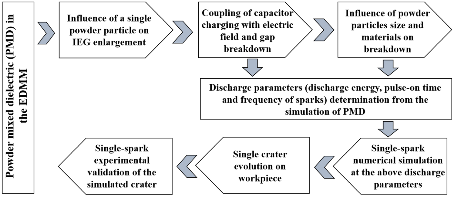
Flow chart presenting the outline of the work.
Numerical simulation
Model description
Figure 2(a) shows a schematic diagram of the EDMM process using PMD during the pulse-off time. As the potential is applied across the electrodes, the powder particles arrange toward the region of the maximum electric field, that is, the notch region, as shown in Figure 2(b). Kerosene having a dielectric strength of 18 MV/m, 19 has been chosen as a liquid dielectric wherein the powder particles are added. The boundary conditions, viz. zero potential and applied electric potential (static and varying), are shown in Figure 2(c).
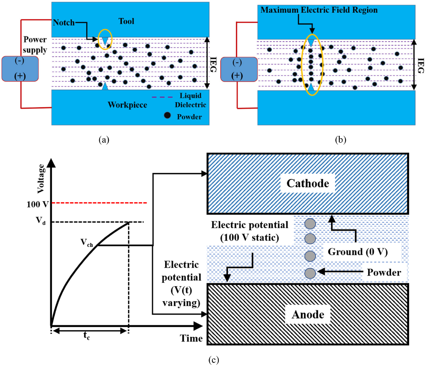
(a) Schematic representation of the EDMM with PMD during the pulse-off period, (b) alignment of powder particles at the point of the maximum electric field during the pulse-on period, and (c) boundary conditions with respect to the static and varying applied voltage.
Figure 3(a) and (b) represent the meshed 2-D domain used for numerical simulation. Extremely fine triangular mesh for electrodes, dielectric domain and manually controlled mesh for powder particles (minimum mesh size of 0.1 μm) have been used. Numerical simulation is performed in COMSOL Multiphysics 5.0®.
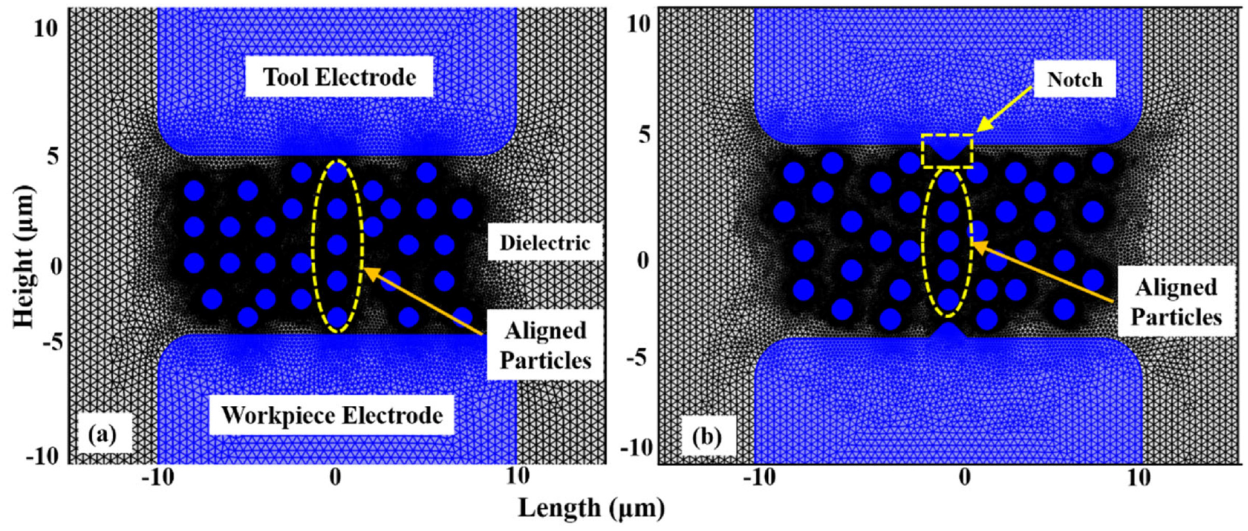
The meshed 2-D domain used for numerical simulation: (a) plain/smooth electrodes and (b) notch electrodes.
Assumptions
The following assumptions are made for the numerical simulation of the EDMM process using PMD:
The powder particles are assumed to be uniformly distributed in the liquid dielectric, that is, there is no sedimentation.
The particles are considered stationary once they enter the IEG for the duration of a pulse.
There is a finite gap (liquid dielectric film) between two particles or between particles and electrodes to avoid short circuits. 20
Energy losses due to the melting or vaporization of particles are ignored.
The discharging time is assumed as 10% of the charging time. 21 The stray capacitance is neglected as it is significantly smaller than the used capacitance (0.47 μF).
For a single pulse input, there is only one spark. Therefore, multiple sparks from a single pulse are ignored.
Governing equations
The charge conservation equation, which assumes no additional charge generation or loss, is given as follows 22 :


where
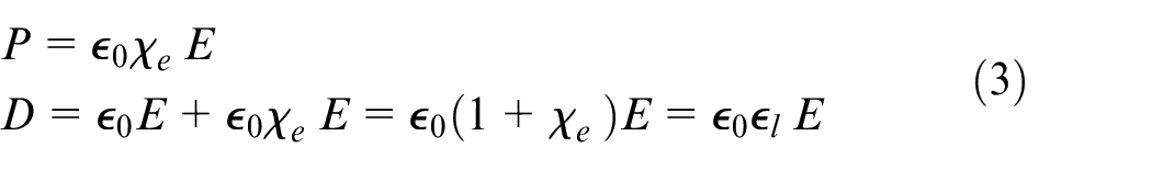
Putting Equation (3) in Equation (1), Equation (1) modifies to take the following form of charge conservation equation:


Results and discussion
Electric field simulation for a single powder particle
When a powder particle is placed in the gap, charge distribution takes place on its surface due to the applied electric field, as per Pauthenier and Moreau-Hanot’s Equation 23 :
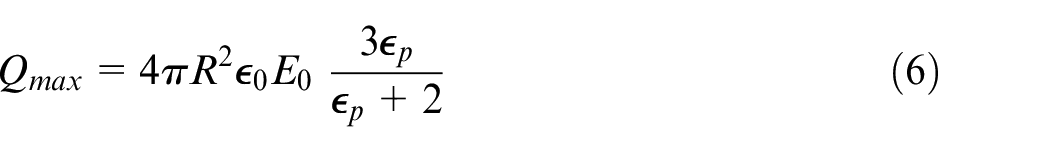
where

where θ is the angle between the direction of the electric field and normal to the particle surface, as shown in Figure 4.
Representation of the variation in the electric field on a powder particle’s surface.
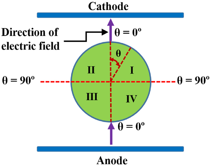
A silicon powder of 1 μm diameter is assumed to be suspended at a distance of 1 µm from the anode. The electric field simulation is performed by applying a static potential of 100 V across the electrodes separated by an IEG of 10 μm. Figure 5 shows the numerically simulated image of a particle wherein the electric field intensification occurs near the point where the applied electric field’s direction and normal to the powder surface are parallel. Subsequently, it decreases to minimum at a 90° angle between the applied field’s direction and normal to the particle’s surface.
Electric field intensity distribution around a silicon powder particle (applied potential: 100 V, IEG: 10 μm, particle diameter: 1 μm).
Inter-electrode gap enlargement due to a single powder particle
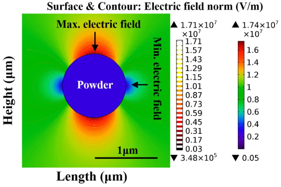
Figure 6(b) depicts the maximum possible IEG between two rounded corner electrodes (filet radius 2 μm) at which the magnitude of the applied electric field is equal to or above the threshold value (Eth: 18 MV/m). The simulation is performed for a constant gap voltage of 100 V while placing a single circular (diameter 1 µm) and elliptical shape particle at 1 μm distance from the anode surface. The major axis of the elliptical-shaped particle is taken as 0.6 μm, and the minor axis (i.e. 0.42 µm) is calculated by keeping the area of the circular (diameter 1 µm) and elliptical particles to be constant. The orientation of these two particles is depicted in Figure 6(a). With the inclusion of a circular and elliptical-shaped particle, the maximum magnitude of IEG for the successful dielectric breakdown is 10.5 and 9.25 µm, respectively, compared to 7.6 µm (∼38% and ∼22% gap enlargement) for pure dielectric. Higher conductive space in the electric field direction accessible with circular particle than the elliptical particle (due to minor axis in the electric field direction) results in the higher electric field with circular shape particle. The minor axis of the elliptical particle is in the direction of the applied field. However, changing the particle’s orientation (major axis in the direction of the electric field) results in slightly higher IEG (∼12.35 µm) at the breakdown (∼63% enlargement) due to higher conductive space. The machining stability in terms of occurrence of normal discharges or prevention of abnormal discharges and efficient cleaning of the gap is possible with the effective removal of debris particles at higher IEG.25,26
(a) Schematic of circular and elliptical powder particle’s orientation in the IEG (scale is different for both particles) and (b) variation of the maximum electric field in the gap with varying IEG (applied potential: 100 V, IEG: 10 µm, silicon particle).
Electric field simulation using multiple powder particles in the gap
Transient variation of electric field and its coupling with gap breakdown
Multiple powder particles (total 35 particles, including 6 bridging particles) are introduced in the IEG of 10 µm, whereas the voltage required for the breakdown of the gap and corresponding charging time is evaluated from the capacitor’s charging characteristics (refer to Figure 2(c)). As the potential is applied across the IEG, the breakdown between two particles or between any particle and electrode occurs (between 1 and 2, in Figure 7). The breakdown causes a short circuit between two particles, and consequently, redistribution of charges occurs (at 3 and 4). In this manner, breakdown propagates and spark formation takes place across the gap due to series of discharges. 27
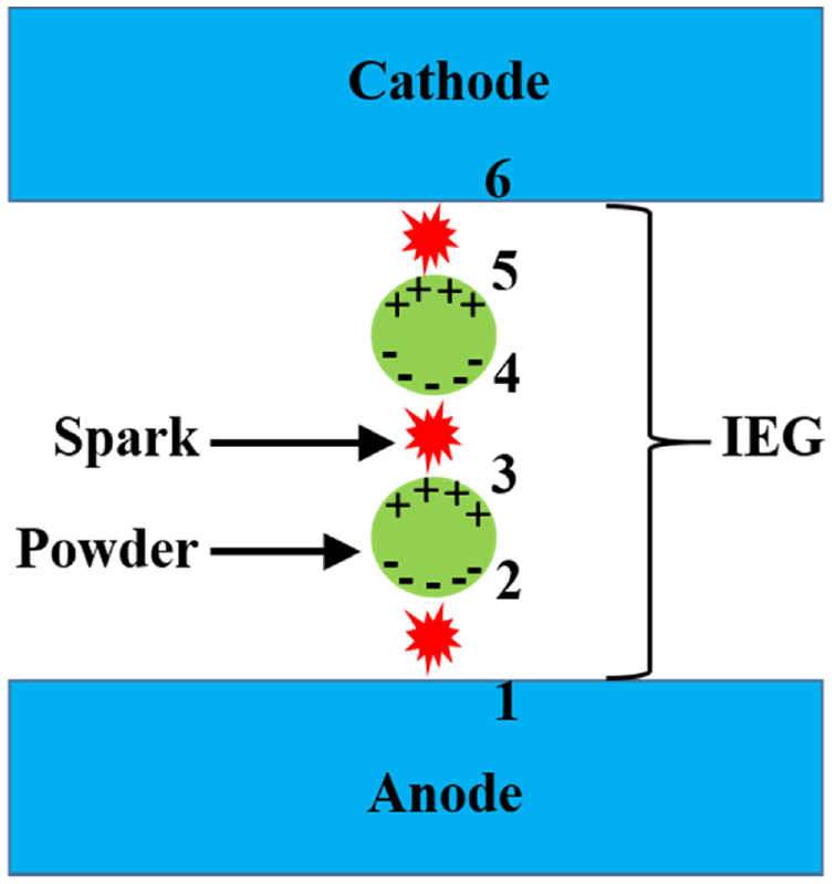
Series discharge with multiple powder particles in the IEG.
Electric field simulation using smooth electrodes
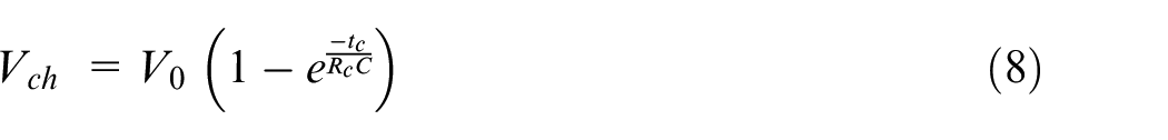
The smooth electrodes refer to the ideal surfaces with no asperities, and the electric field intensity is uniform in the IEG for the pure dielectric except at sharp corners. A model is formulated to describe the variation in maximum electric field strength in the gap with charging (pulse-off period) of the capacitor in resistance-capacitance power generator. The fundamental equation of capacitor charging is given in equation (8). 28 It is coupled with the electric field (equation (5)) in the IEG.
where
Schematic illustration and simulated image of: (a) sharp edges electrodes, (b) rounded edges electrodes (applied potential: 100 V, IEG: 10 μm, particle diameter: 1 μm), and (c) variation of the maximum electric field in the gap with and without filet radius of electrodes for the pure dielectric (open circuit voltage: 100 V, R = 1000 Ω, C = 0.4 μF). R and C are the charging resistance and capacitance, respectively.
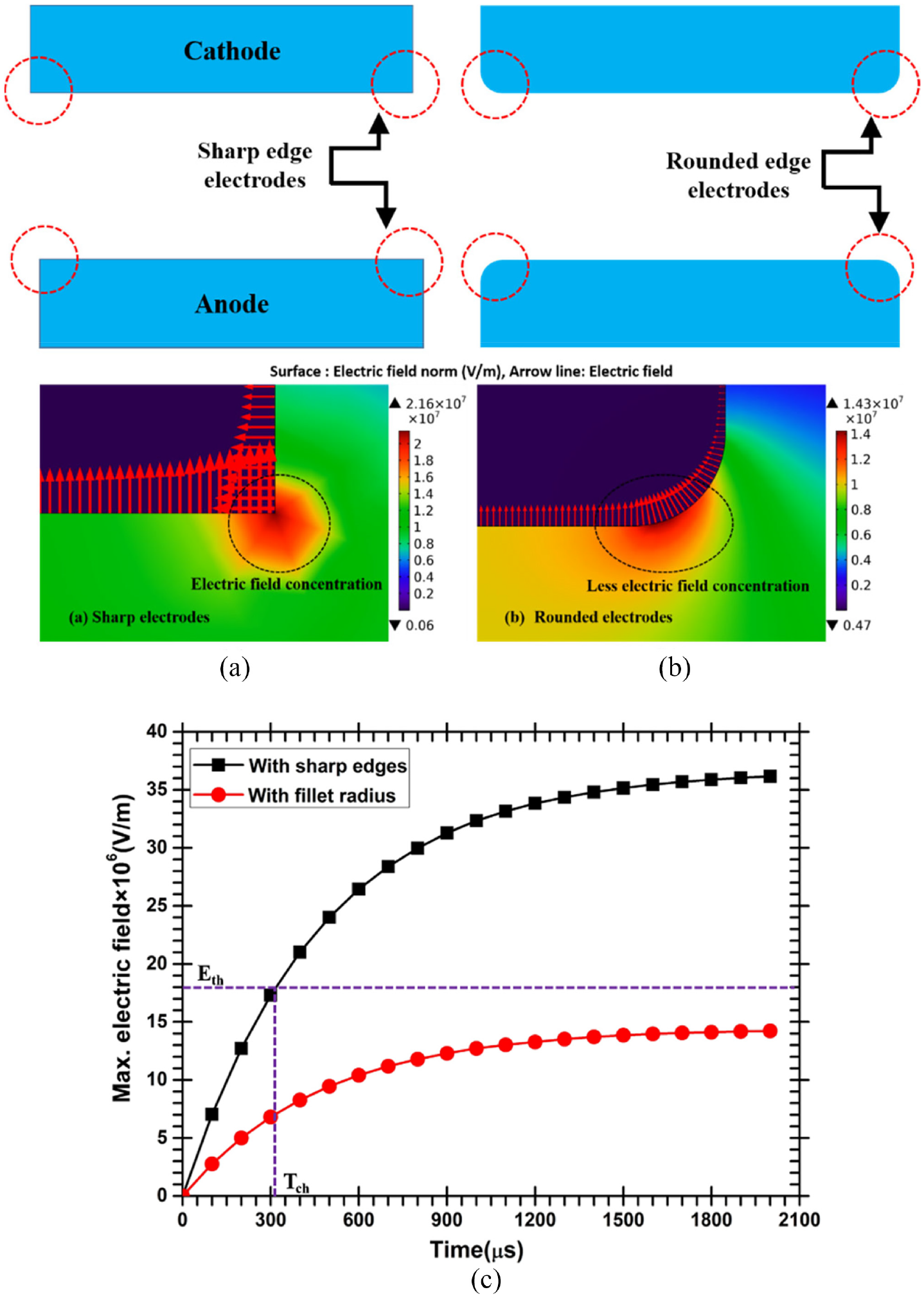
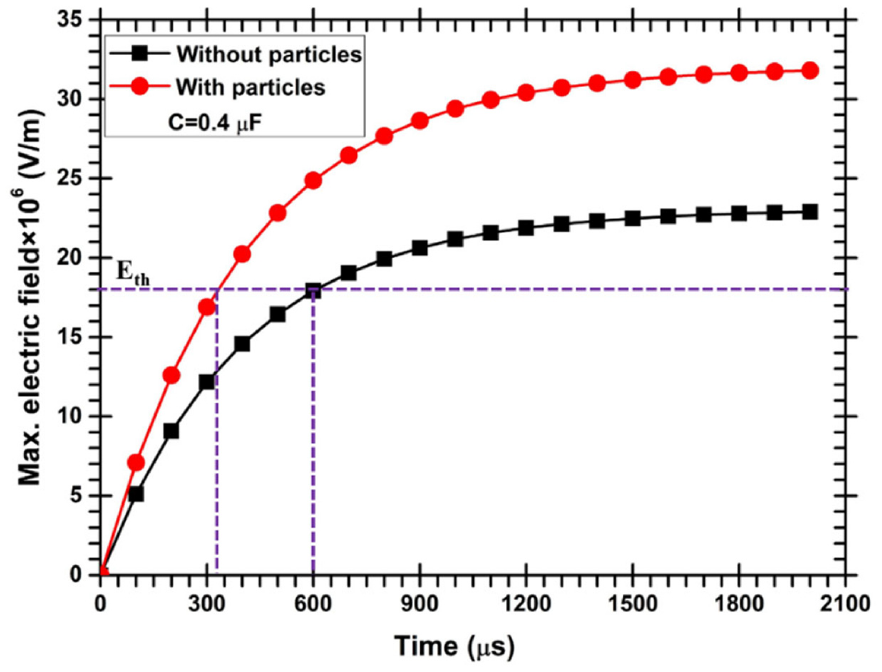
During the initial phase of machining, the maximum electric field strength is concentrated on the electrodes’ sharp edges (approx. three times to the rounded electrodes), and the charging time for breakdown is around 300 μs, in Figure 8(c). However, as the edges of the electrodes erode, they become rounded with a certain radius. It has been observed that the filet radius (2 μm) electrodes without any powder particles hardly attained the breakdown strength of the dielectric (Eth), as shown in Figure 8(c). Therefore, it is concluded that as the machining progresses, the electric field localization near the electrodes edges decreases and it is indispensable to decrease the IEG (poor flushing with smaller IEG). However, using PMD, the breakdown can occur at a lower potential, which reduces the charging time, and there is no need to minimize the IEG. It is evident from Figure 9 that using rounded edge electrodes and PMD, the threshold electric field (Eth) is attained at around 600 μs, which is unachievable in the instance of pure dielectric with the existing IEG (Figure 8(c)).
Variation of the maximum electric field in the gap for rounded (filet radius) electrodes, with and without powder particles (open circuit voltage: 100 V, R = 1000 Ω, C = 0.4 μF, silicon particle of diameter 1 μm).
Electric field simulation using notch electrodes
Further, electrodes with rounded corners (filet radius of 2 μm) and notches at the electrodes’ center are employed for the numerical simulation. The notches show a point of asperity on the electrodes where the probability of discharge is maximum due to the intense electric field, as shown in Figure 10. The particles diffuse to the notch region, forming a chain across it. Subsequently, the spark location switches to another point depending upon the height of asperities, which is not shown in this case. With notch electrodes of filet radius and PMD, the dielectric breakdown strength is achieved at a voltage (58.3 V) and charging time (330 μs) compared to pure dielectric (80.3 V, 600 μs), as shown in Figure 11.
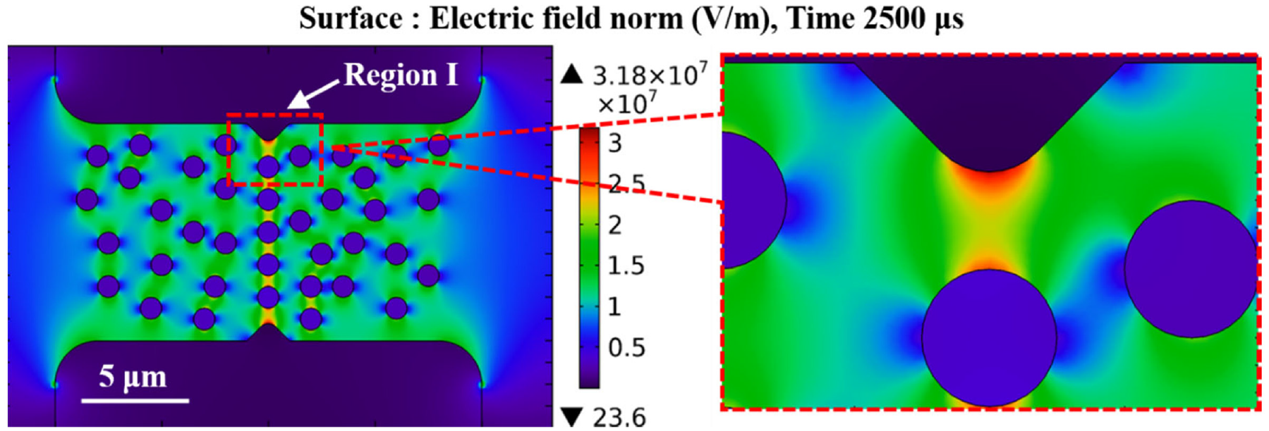
Distribution of electric field in the IEG with PMD and enlarged view of the region I (open circuit voltage: 100 V, R = 1000 Ω, C = 0.4 μF, silicon particle of diameter 1 μm).
Variation of the maximum electric field in the gap with filet radius and notch electrode, with and without powder particles (total 35 particles including 6 bridging particles, open circuit voltage: 100 V, R = 1000 Ω, C = 0.4 μF, silicon particle of diameter 1 μm).
Electric field simulation with varying particles size
The field strength is considerably influenced by the diameter of the particles having a constant spacing between two particles. Larger powder particles result in higher gap widening (higher electric field generation) than the smaller particles due to higher conductive space or lower gap resistivity. 29 Owing to this variation in the electric field, the threshold field strength with 0.3, 0.5, and 1 μm diameter particles is attainable at 460, 425, and 340 μs, respectively, as shown in Figure 12.
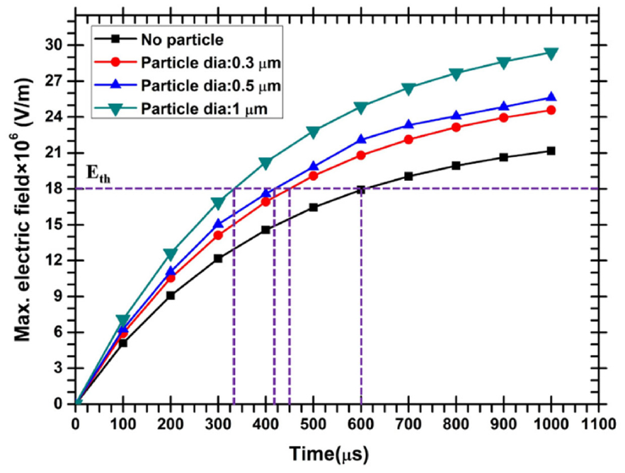
Variation of the maximum electric field in the gap with filet radius and notch electrode for varying particle sizes (open circuit voltage: 100 V, R = 1000 Ω, C = 0.4 μF, silicon particles).
Effect of powder material properties on dielectric breakdown
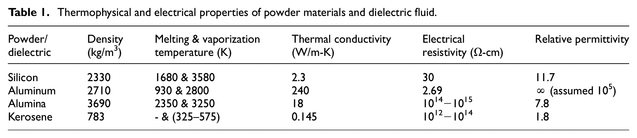
Three powder materials, namely aluminum (Al), silicon (Si), and aluminum oxide/alumina (Al2O3), are selected to evaluate the relative variation in the electric field strength with varying powder materials. Table 1 depicts the pertinent thermophysical and electrical properties of powder materials and dielectric fluid. The relative magnitude of maximum electric field strength during the capacitor’s charging phase is shown in Figure 13(a). Owing to the substantially higher relative permittivity of aluminum, the electric field strength is higher than that achieved using silicon and Al2O3 powder. The corresponding charging time of the capacitor using aluminum PMD is obtained as 275 µs compared to 340 and 360 μs with silicon and Al2O3 particles, respectively. Figure 13(b) depicts the charging time for breakdown (Eth = 18 × 106 V/m) with varying relative permittivity of powder materials. The breakdown voltage for Al, Si, and Al2O3 powder particles is 49.7, 57.23, and 59.34 V, respectively, compared to 80.3 V for the pure dielectric.
Thermophysical and electrical properties of powder materials and dielectric fluid.
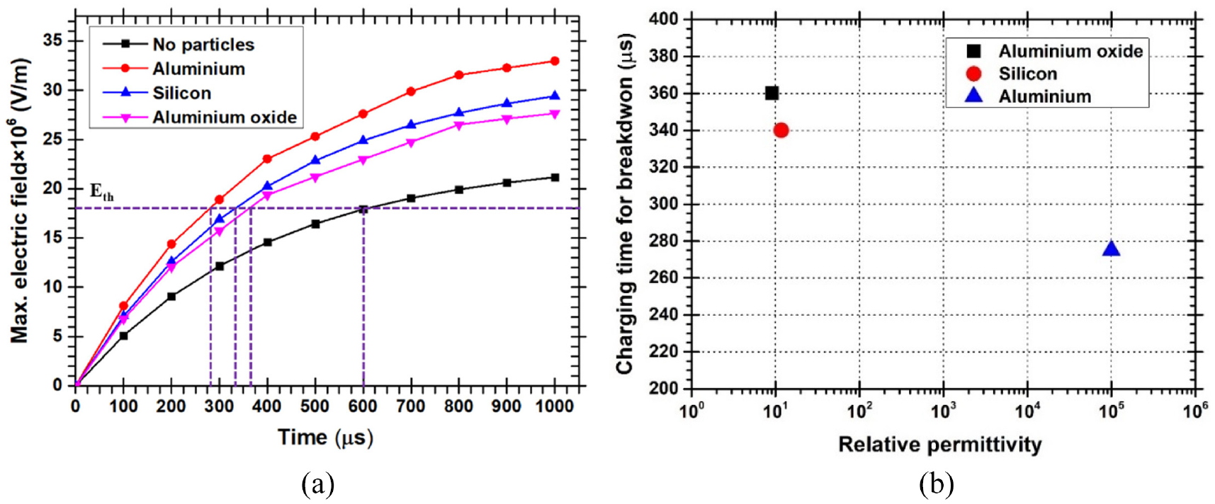
(a) Comparison of electric field intensity for aluminum, silicon and Al2O3 particles of 1 μm diameter and (b) charging time for breakdown (Eth = 18 × 106 V/m) with varying relative permittivity of powder material, abscissa in logarithmic scale (open circuit voltage: 100 V, R = 1000 Ω, C = 0.4 μF).
Numerical simulation (Figure 14) also reveals that the powder particles are effective in minimizing the breakdown voltage/charging time for breakdown compared to the pure dielectric, provided their relative permittivity is higher than that of the host (liquid) dielectric (kerosene in this case), irrespective of their electrical conductivity (Figure 14(a)). However, as the relative permittivity of the powder particles is smaller than that of the liquid dielectric, the electric field distribution is altered, and the maximum intensity is no longer attainable at the particle’s surface (Figure 14(b)).
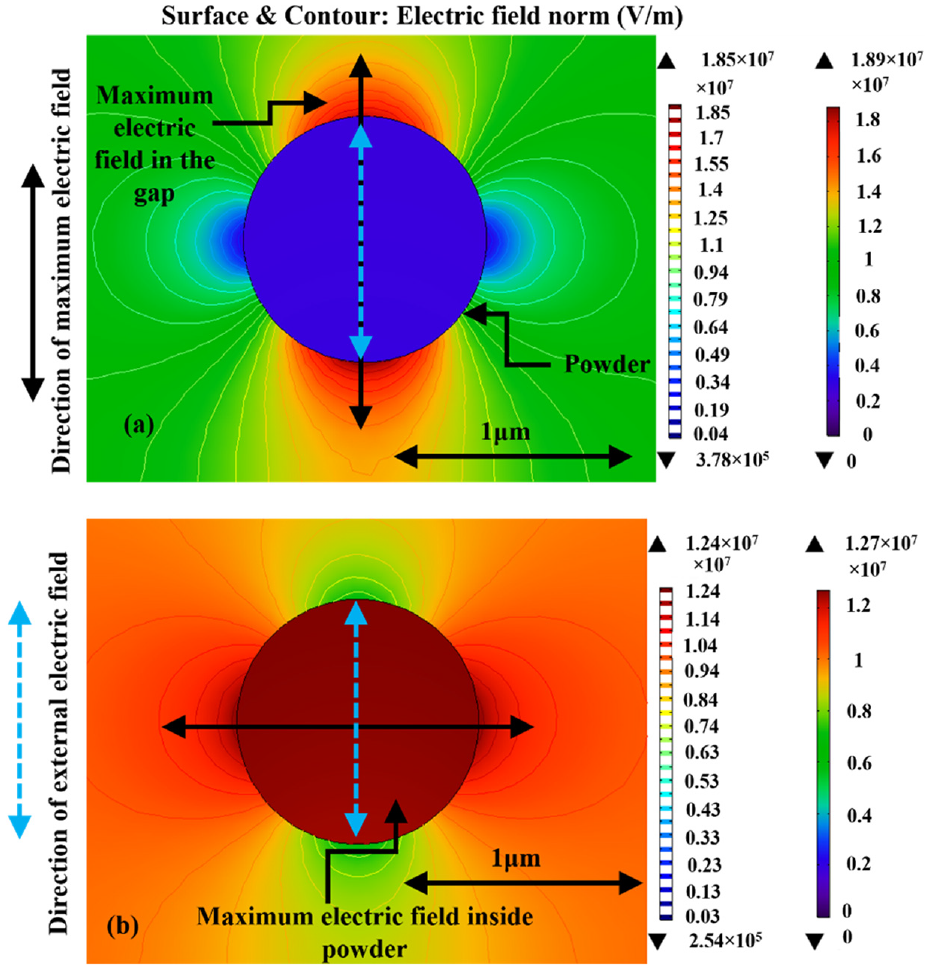
Electric field distribution on a powder particle in the IEG: (a) when the relative permittivity of the particle (11.7) is higher than that of liquid dielectric (1.7) and (b) when the relative permittivity of the particle (1) is lesser than that of liquid dielectric (1.7).
Single-spark numerical simulation of PMD for crater formation
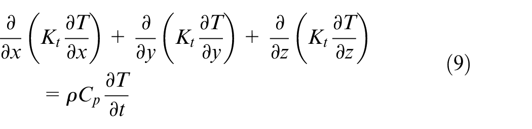
Single-spark numerical simulation is performed using the discharge parameters (Table 2) obtained from the numerical simulation of PMD discussed in the previous sections. Assuming Gaussian distribution of heat flux and thermal conduction of incident heat to the workpiece, the portion of the workpiece material having a temperature above the workpiece’s melting point is removed, that is, assuming the molten metal ejection efficiency to be 100%. 30 The incident heat flux to the workpiece is conducted as per the following heat conduction equation:
Inferred input parameters from the electric field simulation of PMD.
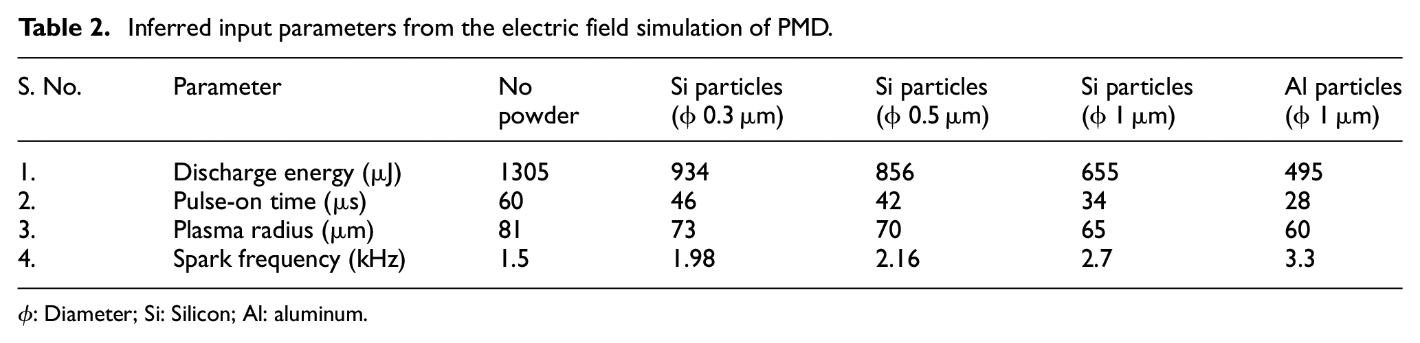
ϕ: Diameter; Si: Silicon; Al: aluminum.
where
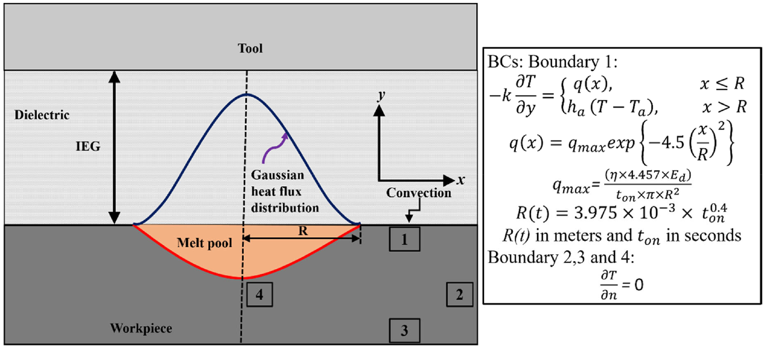
Schematic illustration of the 2-D domain used for single-spark numerical simulation and associated boundary conditions.
In Figure 15, T and T
a
are the surface and ambient temperature,
The normal velocity of the surface deformation (workpiece erosion) is calculated based on the convective heat flux during the pulse-off period. Additional details pertaining to the creation of a single crater are provided in Singh et al. 35 Figure 16 shows images of the numerically simulated single crater in various cases of dielectric. The crater depth is overpredicted due to the 100% flushing efficiency of the molten metal. Whereas in actual machining conditions, the flushing efficiency is as small as ∼30%–35%. 36
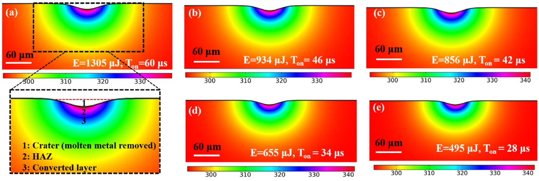
The numerically simulated single crater at varying dielectric conditions: (a) no powder, (b) Si powder of 0.3 μm diameter, (c) Si powder of 0.5 μm diameter, (d) Si powder of 1 μm diameter, and (e) Al powder of 1 μm diameter (scale: surface temperature in K, E = discharge energy, Ton = pulse-on time).
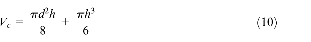
The approximate volume of a single crater
The output parameters determined from the single-spark numerical simulation are given in Table 3.
Output responses from the single-spark numerical simulation using the discharge parameters given in Table 2.
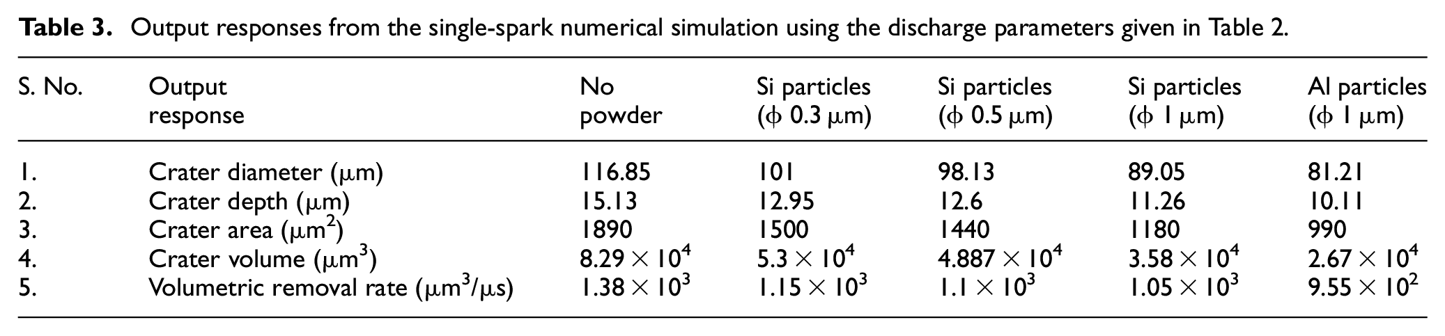
The crater diameter and depth decrease with PMD (Table 3 and Figure 17(a)) due to a reduction in discharge energy and pulse-on time of a pulse. Similar experimental results of a decrease in crater diameter and depth using PMD were reported in Yeo et al. 38 and Talla et al. 39 The output responses evaluated in Table 3 and Figure 17(a) reveals that with the addition of powder particles in the liquid dielectric, the volumetric material removal rate decreases (∼30.8% reduction from no powder to Al particles of ϕ 1 µm). However, the increased frequency of sparks (∼120% increase from no powder to Al particles of ϕ 1 µm), as shown in Figure 17(b), with PMD eventually compensates or surpasses the reduction in crater volume per spark, resulting in higher machining rate. 40
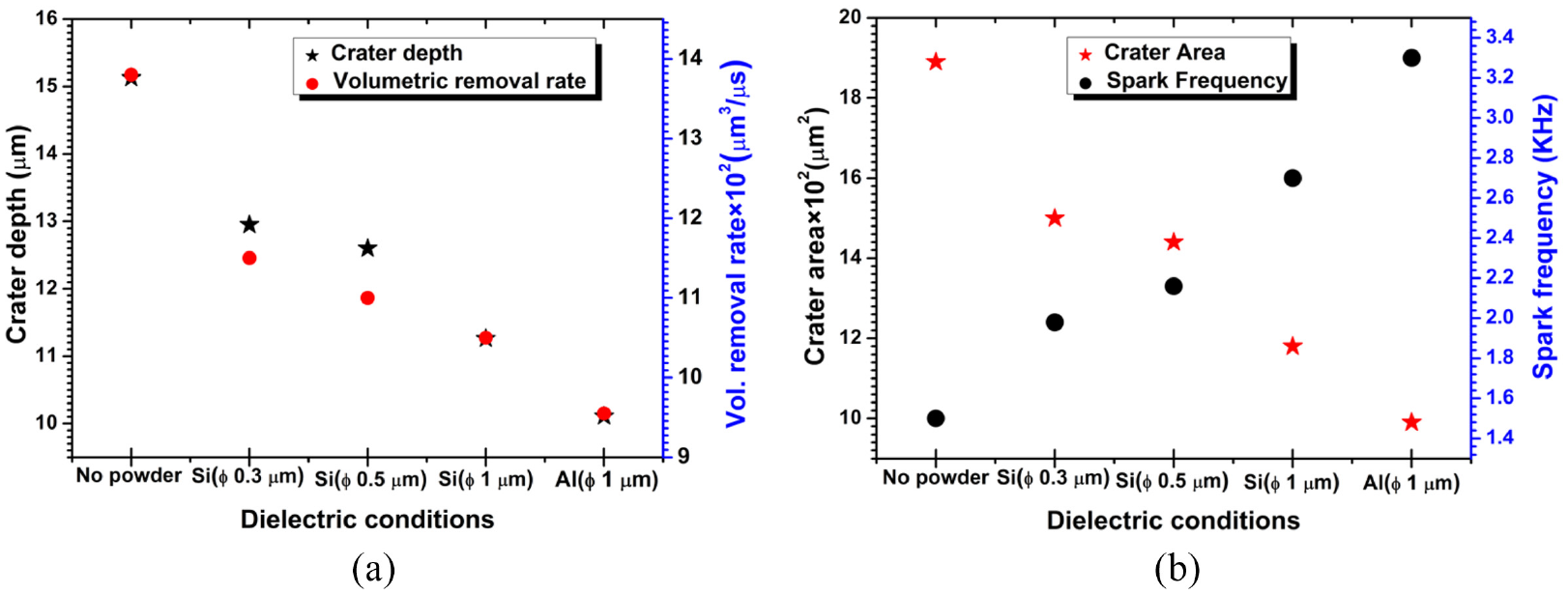
Variation of: (a) crater depth and volumetric removal rate and (b) crater area and spark frequency with the varying conditions of the dielectric (ϕ: diameter, Si: silicon, Al: aluminum).
Model validation
Single-spark experimentation of PMD
Single-spark experiments are performed using a dedicated capacitor-based single-spark circuit integrated with the micro-EDM machine tool: DT-110 (make: Mikrotools Singapore), as shown in Figure 18(a). Copper plate and tungsten carbide rod of diameter 300 μm have been used as workpiece and tool, respectively. Hydrocarbon dielectric (EDM-Oil) is used as a host dielectric fluid in which powders are added. Figure 18(b) depicts the captured single-spark generated in the IEG using PMD.
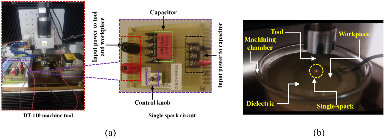
(a) Capacitance-based single-spark power generator integrated with DT-110 machine tool and (b) single spark captured in the gap submerged with PMD.
With aluminum and alumina powder particles of an average diameter 1 μm, the breakdown of the gap is attainable up to 70 μm and 42 μm compared to 26 µm with pure dielectric (∼170% and ∼62% increase in IEG with aluminum and alumina), as shown in Figure 19. Compared to powder concentration of 1 g/l, the IEG enhances at 2 g/l because of the higher electrical conductivity of the PMD and lower dielectric strength of the dielectric. However, further increase in powder concentration to 3 g/l, agglomeration and settling of powder result in slightly lower IEG at the breakdown. Short-circuits can also occur beyond a certain powder concentration. 41 Therefore, the highest IEG is attained at the medium concentration (2 g/l). Figure 20(a)–(i) show the optical image, 3-D image and line graph of the single crater formed on the copper workpiece using a pure dielectric, aluminum PMD and alumina PMD. The average diameter and depth of the crater (five craters/repetitions at each concentration) are found to be 62 and 8.2 μm and 69 and 11 μm (standard deviation of ±5 and ±0.6 μm, respectively, for diameter and depth), respectively with aluminum and alumina PMD compared to pure dielectric (average diameter 92 μm and depth 13.3 μm). The reduction in crater’s dimensions confirms a reduction in discharge energy of a pulse in PMD compared to the pure dielectric, as also revealed by the numerical simulation. Thus, it validates the results of numerical simulation showing the effectiveness of aluminum and alumina PMD.
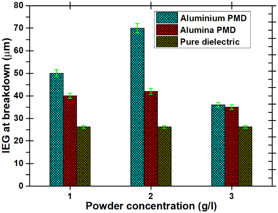
Measured IEG at the breakdown with different dielectrics.
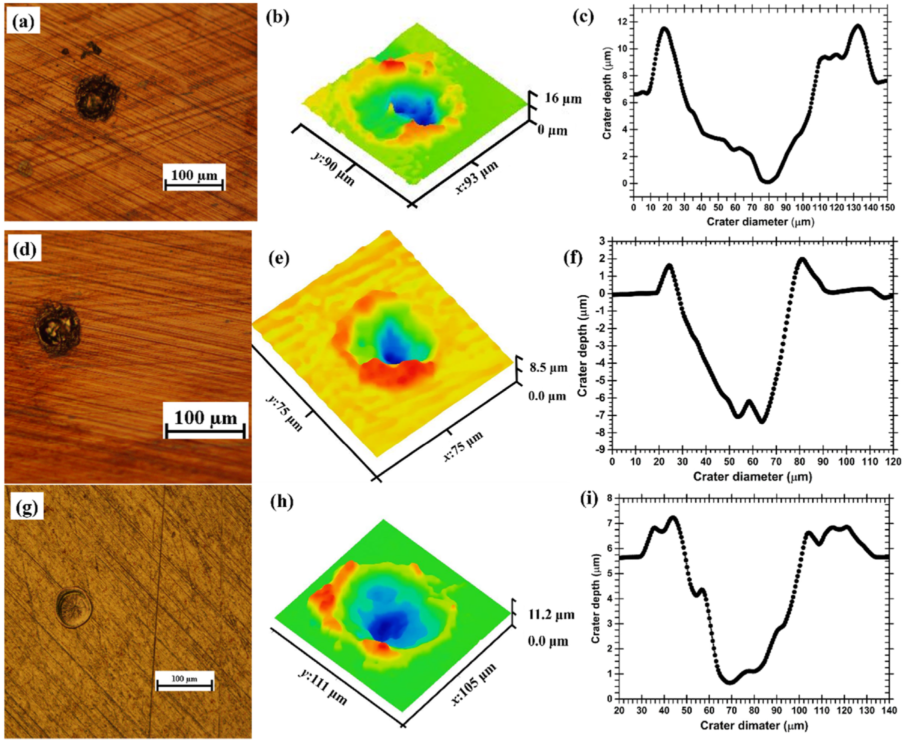
Optical, 3-D image and line-graph of a single crater formed on the copper workpiece: (a)–(c) using pure dielectric, (d)–(f) using aluminum PMD, and (g)–(i) using aluminum oxide PMD (capacitance: 0.47 μF, voltage: 96 V).
Multi-spark experimentation of PMD
Performing micro-dimples machining (i.e. multi-spark machining) using pure dielectric, alumina PMD and aluminum PMD, the surface of the machined dimples is analyzed. Figure 21 shows the 3-D profilometer and Scanning Electrons Microscope (SEM) image of the machined dimples with different dielectrics. The SEM images of the machined dimples confirm surface uniformity with aluminum and alumina PMD compared to the pure dielectric. Moreover, the surface roughness (Ra) value (determined from the 3-D profilometry) of the machined dimples with pure dielectric is highest (2.01 µm), followed by alumina PMD (1.88 µm) and aluminum PMD (1.43 µm), depicting the role of PMD in obtaining a smoother surface due to lower crater depth, as also predicted by the numerical simulation.
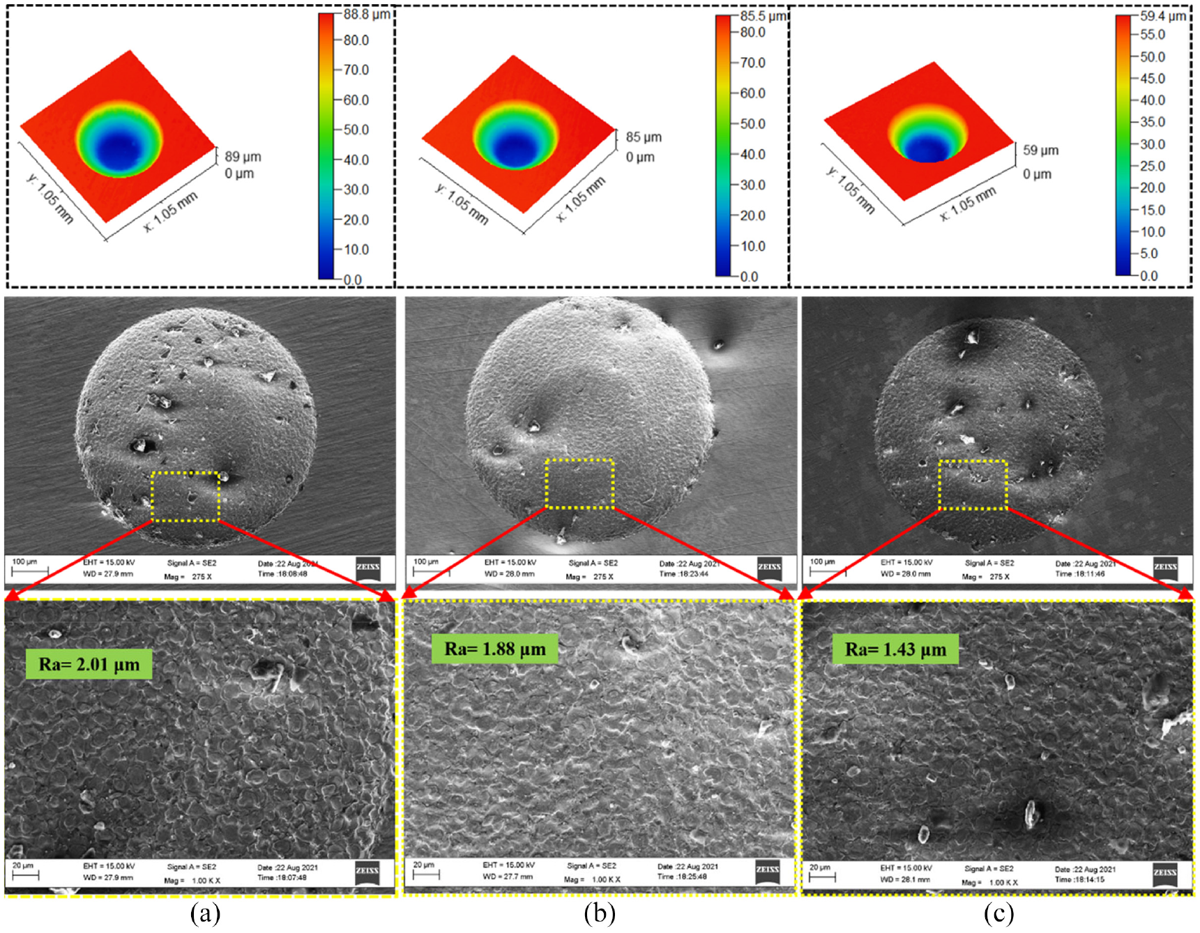
3-D profilometer and SEM micrograph of the machined dimples using: (a) pure dielectric, (b) alumina PMD (1 g/l), and (c) aluminum PMD (1 g/l).
Validation of numerically simulated craters
The numerically simulated single craters’ dimensions (diameter and depth), as discussed in the previous section (Single-spark numerical simulation of PMD for crater formation), are validated with single-machined craters. The required levels of discharge energies corresponding to different powder materials and sizes, as shown in Table 2 (row 1), are obtained by changing the charging voltage for a constant capacitance value of 0.47 μF. Figures 22(a)–(e) and 23(a)–(e) show the optical and 3-D images of the single craters formed at different discharge energy settings.
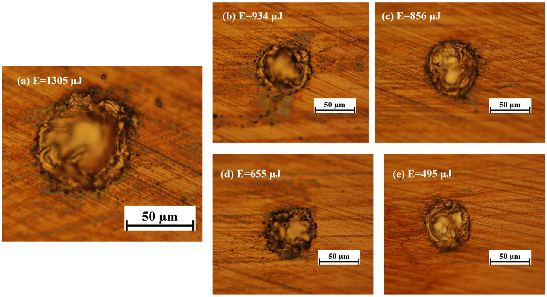
Optical images of a single crater formed at discharge energy obtained through numerical simulation: (a) no powder, (b) Si powder of 0.3 μm diameter, (c) Si powder of 0.5 μm diameter, (d) Si powder of 1 μm diameter, and (e) Al powder of 1 μm diameter.
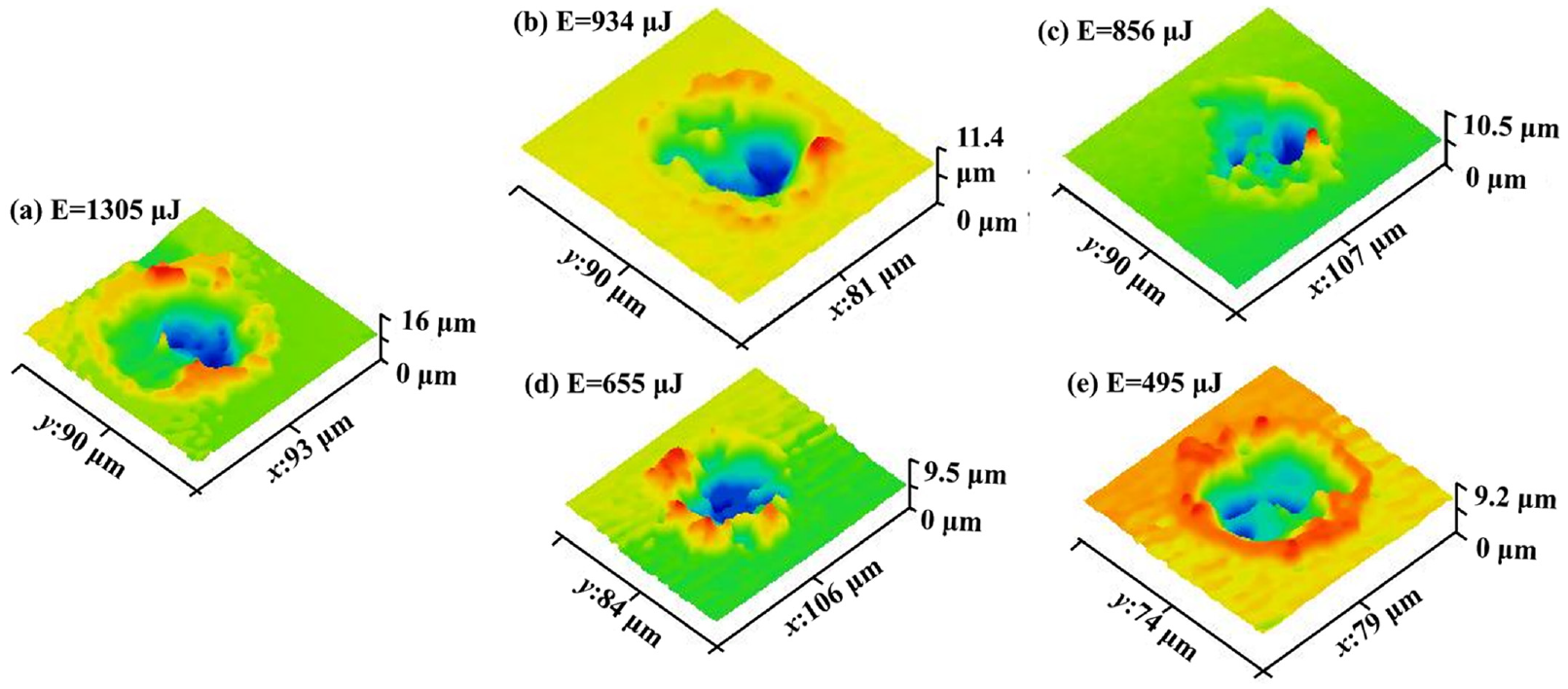
3-D images of a single crater formed at discharge energy obtained through numerical simulation: (a) no powder, (b) Si powder of 0.3 μm diameter, (c) Si powder of 0.5 μm diameter, (d) Si powder of 1 μm diameter, and (e) Al powder of 1 μm diameter.
Figure 24(a) and (b) represent the comparative analysis of crater diameter and depth from numerical simulation and single-spark experiments (average of five repetitions at each level). The simulated crater diameter and depth are slightly higher than those measured in experiments. It can be explained by the 100% flushing efficiency assumed in the numerical simulation, which is not attainable in the real EDMM conditions due to inadequate flushing of liquid metal and recast layer formation. 42 Some other simplifying assumptions (plasma channel radius and energy fraction to the workpiece) also contribute to higher crater dimensions in numerical simulation. Nonetheless, a close prediction and trends of crater dimensions confirm the utility of the single-spark numerical model of PMD.
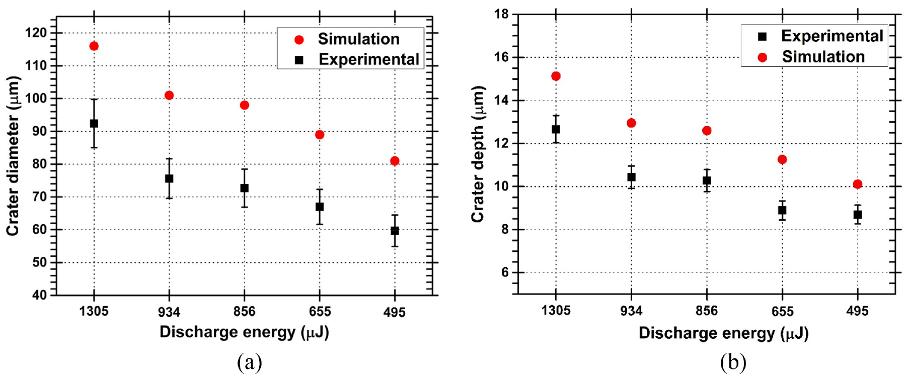
Comparison of: (a) crater diameter and (b) crater depth, obtained from single-spark numerical simulation and single-spark experimentation.
Conclusions
An attempt has been made to comprehend the mechanism of powder mixed dielectric in the electrical discharge micromachining process through electric field numerical simulation. Some of the significant conclusions deduced from the present work are as follows:
The percentage increase in inter-electrode gap for breakdown with a circular and elliptical silicon particle is ∼38% and ∼22%–63%, respectively, with regard to the pure dielectric.
Numerical analysis revealed that powder particles having relative permittivity higher than the host dielectric are effective in electrical discharge micromachining. Therefore, electrically non-conductive alumina powders mixed in kerosene dielectric have been proven effective due to their higher relative permittivity than kerosene.
Single-spark numerical simulation predicts a reduction in crater volume with the addition of powder particles. However, the increased frequency of sparks (maximum increase of ∼120%) results in higher material removal rate and a better-finished surface.
A significant enlargement in the inter-electrode gap (∼170% and ∼62% with aluminum and alumina powder mixed dielectric) at the breakdown is attained compared to pure dielectric during single-spark experimentation.
Numerically simulated crater dimensions at varying powder material and sizes are slightly higher (deviation in crater diameter ∼20%–25% and crater depth ∼14%–20%) than those obtained from the single-spark experiments, possibly due to the 100% flushing efficiency and simplifying assumptions made in numerical simulation.
Numerical simulation of powder mixed dielectric in electrical discharge micromachining is expedient in evaluating the discharge parameters based on electric field numerical simulation. Subsequently, by adopting these parameters, the performance of the powder mixed dielectric can be analyzed through the comparisons of machined crater with pure dielectric and powder mixed dielectric. Electric field simulation and crater formation based on the output of electric field simulation results can be coupled for an advanced understanding of the powder mixed dielectric. In addition, spectroscopy analysis of powder mixed dielectric can further enhance the understanding of material removal behavior through the estimation of electrons density and plasma temperature.
Footnotes
Appendix
Declaration of conflicting interests
The author(s) declared no potential conflicts of interest with respect to the research, authorship, and/or publication of this article.
Funding
The author(s) received no financial support for the research, authorship, and/or publication of this article.