
Abstract
The goal of this study has been to establish a method for quantifying the minimum chip thickness, h1min, during longitudinal turning of duplex stainless steel, and explore how the value of h1min changes with varying process parameters. Based on experimental results, it was found that the tool edge radius only has a limited influence on the size of h1min up to a certain feed level after which the chip flow direction close to the nose radius will have an increasingly pronounced effect. Experimental results show that h1min may be as large as 40% of the theoretical chip thickness when machining duplex stainless steel, results which were corroborated by an finite element method (FEM) analysis. Thus, it can be concluded that a substantial amount of workpiece material will only be deformed onto the machined surface or will form the side flow and not removed as a chip.
Keywords
Introduction
Duplex stainless steel (DSS) is ferritic–austenitic dual-phased alloy with an attractive combination of high mechanical strength, good corrosion resistance and relatively low cost compared to other stainless steels contributing to making DSS one of the fastest growing stainless steels. 1 DSS is used in many applications in the processing industries, especially when localized corrosion is a potential problem. 2 Today, DSS is used in desalination plants, chemical tankers, pressure vessels, storage tanks, tanks and machinery for the pulp and paper industry, and civil engineering. 3 Stainless steels are generally considered to have a low machinability due to high tensile strength, high work hardening rates, high fracture toughness and low thermal conductivity. 4 As observed by Krolczyk and Legutko, 5 machining of DSS commonly results in a combination of adhesive and abrasive wear of the cutting tool. However, Larsson and Lundqvist 6 argue that DSS is not necessarily more difficult to machine than austenitic stainless steel given proper selection of process conditions. Due to the known correlation between surface roughness and corrosion resistance, 7 careful consideration of the workpiece surface integrity during machining operations is advisable.
The minimum chip thickness, h1min, is defined as the lowest value of the theoretical chip thickness at which a chip is still formed by the machining process. During any machining process, the dimensions of the minimum chip thickness parameter are highly relevant as they correlate to the amount of material plowed onto the workpiece surface. This is mainly influenced by the workpiece material elastic–plastic properties, the cutting edge geometry and machining process kinematics.8,9 The size of h1min is also closely related to the location of the stagnation point defined as a separation point of the two material flows forming the chip and the machined surface. Consequently, h1min can be used to describe the deformation of the machined surface and its influence on the workpiece surface integrity.10–16
Several analytical efforts have been published on the size and importance of h1min.10,12–17 However, only a few methods to experimentally determine h1min have been published.17–19 De Oliveira et al. 20 proposed an experimental method; however, the indirect nature of optically examining the machined surface texture decreases the practical usability. Przestacki et al. 9 proposed a model through which the cutting forces are used to calculate h1min. However, this approach inhibits the possibility of studying how h1min varies as a function of the process parameters, particularly h1. Thus, there is still a need for a reliable experimental method for measuring h1min.
Minimum chip thickness h1min
The effects of the cutting process on the surface integrity of the finished part have gained significant interest during latter years.21–25 Several studies have been published on the size and influence of h1min for different machining operations. Yuan et al. 13 conclude that the tool edge radius rβ has a major influence on the size of h1min. Similarly, Yen et al. 14 conclude that a strong relationship between the tool edge micro geometry (edge radius and chamfer) and the size of h1min exists. Yen et al. 14 operate with stagnation angle parameter, θs, which defines the location of the stagnation point h1min (Figure 1). Yen et al. 14 state that when machining AISI 1020 with uncoated cemented carbide tools, the stagnation angle varied between 57° and 65°.
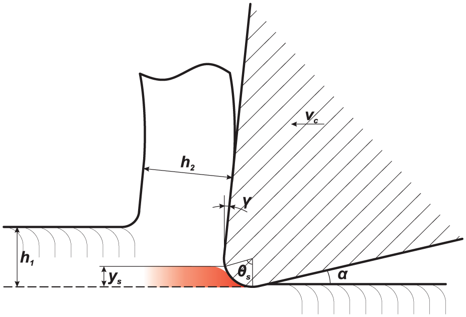
Principle definition of the stagnation angle, θs, and the location of the stagnation point, ys.
Kishawy et al. 15 used a finite element simulation to analyze the mechanics of a machining process through observing the shear stress direction. Based on this modeling approach, the reported stagnation angle was within the range of 61°–71°. Moneim 26 published a model for calculating the location of the stagnation point as a function of the tool edge radius and the friction between the cutting tool and the workpiece. Through analytically modeling the cutting energy, Basuray et al. 18 determined the size of the stagnation angle as θs = 37.6°. Later, Son et al. 17 published an equation for calculating h1min, including the friction between the workpiece and the cutting edge. The variation of process properties along the cutting edge was investigated by Moufki and Molinari. 27 As expected, their results show that the shear strain in the outer edge of the primary shear zone increases distinctly when approaching the location of h1min.
The results of the analytic models indicate the range of stagnation angle within roughly 35°–70°. Therefore, the current study aims to develop a method for experimental measurement of h1min and to examine the influence of selected process parameters on its dimensions. In this study, the size of h1min was measured for LDX 2101, SAF 2205 and SAF 2507 grades of DSS. The experimental results were also corroborated with a finite element modeling investigation.
Method for measuring h1min
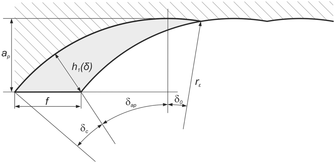
A novel method for measuring the size of h1min has been developed based on the assumption that the theoretical chip thickness, h1, at some point along the tool nose radius, rε, must be equal to h1min as exemplified in Figure 2. Figure 2 illustrates the theoretical chip area, A, as seen from the reference plane, that is, the axial–radial plane for longitudinal turning. The figure also illustrates the two consecutive revolutions of the workpiece during which the tool travels the distance of the feed f. As illustrated in the figure, the existence of h1min will imply that a minor amount of material will not be cut and is therefore plowed onto the machined surface, Apl.
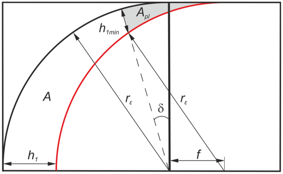
Theoretical chip cross-section geometry at the tool nose radius as seen from the reference plane, adapted from Ståhl. 10
In a machining process, the material flow does separate into two parts, the machined surface and the chip. The part flowing up over the rake surface of the cutting tool forms the chip, while the remainder will flow under the cutting edge toward the workpiece bulk, thus forming the machined surface. This flow separation implies the existence of a stagnation zone or stagnation point. Such point defines the minimum chip thickness h1min. In cases where the theoretical chip thickness h1 is smaller than h1min, no chip will be formed and the material will be plowed under the cutting tool.
For longitudinal turning with a major cutting edge angle of κ = 90°, a theoretical chip cross-section geometry can be perceived at the nose radius of the cutting tool as indicated in Figure 2 assuming machining case A, Figure 3. This condition will imply a restriction on the feed, f, in relation to the tool nose radius, rε, and minor cutting edge angle, κb, limiting the validity of the model, equation (1)

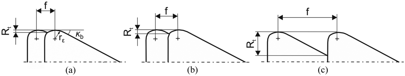
Principle illustration of three different combinations of feed and nose radius resulting in different machining cases where (a) two nose edges, (b) a minor cutting edge and a nose edge, and (c) a minor and a main cutting edge generate a surface. Adapted from Puhasmägi. 28
The red arc in Figure 2 shows the surface that is cut by the tool nose on its current pass and the black arch shows the surface that will be generated one revolution later. To determine the size of h1min, a model pertaining to the geometrical relations at the tool nose radius must be introduced. Based on the work published by Brammertz, 29 the angular position δ is used to determine different locations along the nose radius of the cutting tool. At a certain value of δ, δh1min, the value h1(δ) will be equal to h1min, Figure 2. Thus, knowing δh1min, it is possible to calculate h1min. By considering geometric relations in Figure 2, equation (2) was obtained by Ståhl 10 for varying feed, f, and tool nose radii, rε. A similar solution has also been published by Karpat and Özel 12
Chip flow angle
The chip flow angle, νch, describes the plastic flow direction of a chip during a machining process. The value of zero is assigned to a flow direction which is parallel to the machined surface. Section “Influence of process parameters on h1min” demonstrates that such νch parameter has direct influence on h1min and therefore requires accurate description. Several approaches on calculating νch are known, where Spaans 30 model is the most common. Yet Spaans equation is valid only for straight edge geometry and does not include the tool nose radius. A geometric model by Colwell 31 covers the impact of nose radius, but operates with zero rake and inclination angles only. Along the nose radius, the theoretical chip thickness will become increasingly smaller, Figure 2. Thus, it is expected that thinner chip section will have a smaller relative impact on the flow direction as compared to the other thicker parts of the chip. To include this effect, Ståhl 10 proposed a new equation, equation (3), for calculating νch. The variables involved are geometrically defined in Figure 4 for the case of ap ⩽ rε and κ = 90°

Chip area for ap < rε as seen from the reference plane, adapted from Ståhl. 10
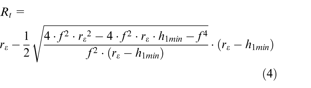
Having the minimum chip thickness region in focus, it can be assumed that the local chip flow angle in h1min zone will have more direct impact on its value than the total chip flow angle for the entire chip. Thus, the conventional models for calculating the overall chip flow νch need to be adapted to investigate the local chip flow direction in the region of interest. The proposed solution to this problem is to set the depth of cut in equation (3) equal to the Rt surface roughness while calculating the chip flow direction, Figure 5. It is possible to derive an expression for the surface roughness Rt for given h1(δ) equaling to h1min. This relationship, similar to Brammertz 32 approach, is presented below in equation (4). Thus, a combination of equations (3) and (4) give a local chip flow directly in h1min region
Schematic illustration of the local chip flow angle, νch, for the uncut material.
Experimental and numerical investigations
Experimental investigation
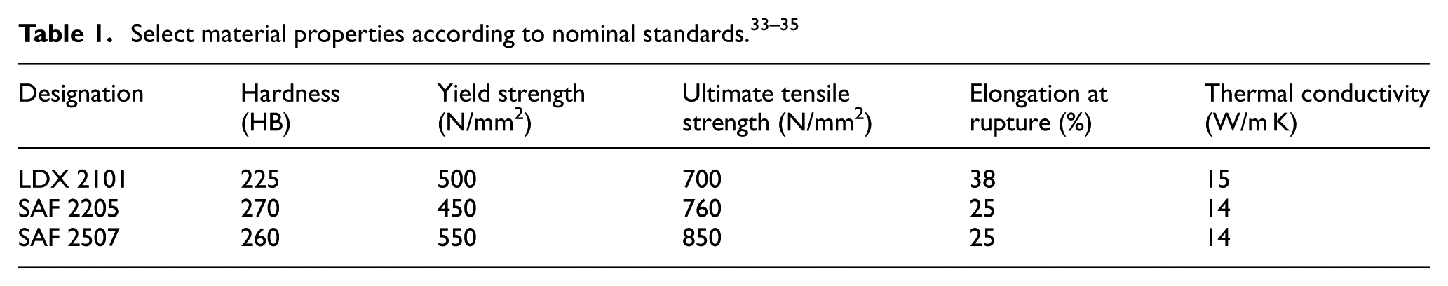
Three different DSSs were machined as part of the current investigation: LDX 2101, SAF 2205 and SAF 2507. Although all the investigated materials belong to the same DSS material group, they significantly differ in terms of properties; the most noteworthy is ultimate tensile strength. Selected relevant material properties for the used steel grades are given in Table 1.
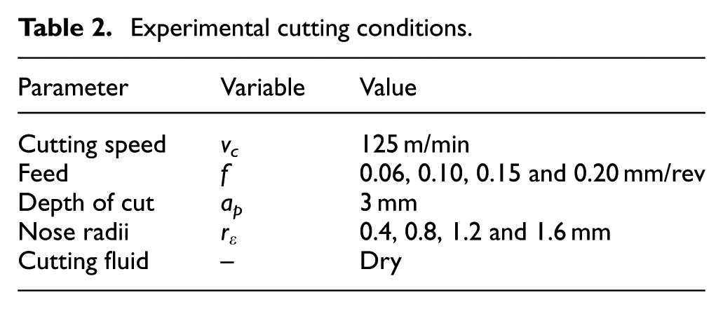
All machined materials were supplied as round bars having a diameter ranging from about 100 to 150 mm. The three materials were machined using Ti(C,N) and Al2O3-coated cemented carbide CNMG120412 cutting tools. The majority of the cutting tools had a nose radius of rε = 1.2 mm. The nose radius was also varied from rε = 0.4 mm to rε = 1.6 mm (Table 2). The inserts were mounted in a DCLNR2525M12 tool holder giving a major cutting edge angle κ = 95°, rake angle γ = 4° and clearance angle α = 6°. No cutting fluid was used during the experiments. Krolczyk et al. 36 have found that dry machining of DSS is a viable option. The cutting conditions used for the experiments are summarized in Table 2.
Experimental cutting conditions.
The obtained chips were measured with two different measuring techniques. Three to four randomly selected chips from each set of cutting parameters were mounted for examination with light optical microscopy (LOM). A second measurement method used involved measurement of the width of chips with a blade micrometer.
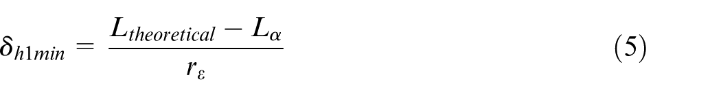
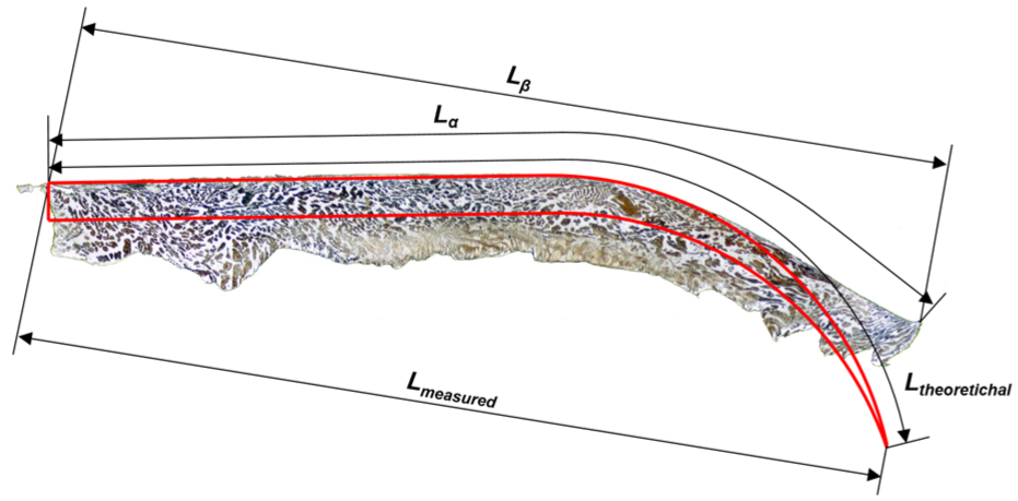
Using equation (2), h1min can be calculated for a known value of δh1min. To determine the size of δh1min, that is, the angle δ for which h1(δ) = h1min, the total theoretical distance along the chip edge, Ltheoretical, must be calculated and then compared to the equivalent distance measured on the acquired chips, Lα, as principally illustrated in Figure 6. By comparing the width on the real chip Lα as compared to the theoretical distance Ltheoretical, δh1min can be determined for a known tool nose radius rε, equation (5)
Cross-section of a chip, perpendicular to the chip flow direction, SAF 2205 at vc = 125 m/min, f = 0.20 mm/rev and ap = 3 mm, compared to the theoretical chip area.
Knowing the value of δh1min, the size of h1min can be calculated based on equation (2) for a known tool nose radius rε and feed f. For each test conditions, LOM measurements were implemented, enabling the measurement of the distance Lα as illustrated in Figure 6. The corresponding number of LOM measurements was 3 to 4. This measurement method is however very time-consuming due to extensive sample preparation and tedious measurement processes. Thus, additional measurements were done using a blade micrometer screw gauge for measuring the width Lβ of the obtained chips. Using this measuring method, a large amount of measurements was obtained enabling a larger statistical basis for further analysis. For all experimental h1min measurements presented in this article, 100 random measurements were made using this second measurement method. However, the micrometer screw gauge measurement method might have a disadvantage; the measured distance will no longer be of the sought distance along the surface of the chip, Lα, but rather the shortest distance between the two sides of the chip, Lβ. To quantify a potential error due to this simplification, an analytical comparison between the two different measuring methods was performed. Assuming that the obtained chips retain their theoretical cross-section geometry, the distance along the chip surface, Ltheoretical, can be compared with the shortest distance between two sides of the chip, Lmeasured, Figure 6. The ratio of Ltheoretical to Lmeasured introduces a correction factor χcorr indicating a potential error, equation (6)
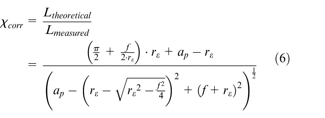
Typically, χcorr obtains values in the range of roughly 1.0 ⩽ χcorr ⩽ 2.0 for normal machining conditions, indicating a risk for measurement errors. However, as evident in Figure 7, the chips were not found to retain its theoretical geometry after the machining process. Instead, machined chips are commonly deformed, obtaining a straightened cross-section. Thus, the measurements performed with a micrometer are more accurate. Based on experimental LOM measurements, the ratio Lα/Lβ was found to be in the range of 0.93–1.06.
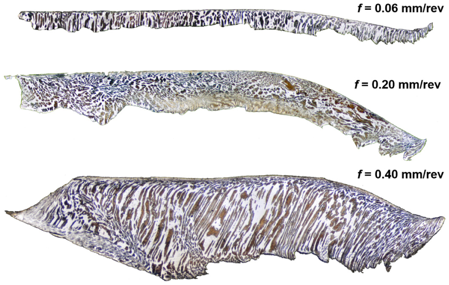
Cross-section of chips perpendicular to the chip flow direction, SAF 2205, for varying feed at vc = 125 m/min and ap = 3 mm, adapted from Schultheiss et al. 19
Another potential source of errors is the chip widening that occurs during all metal cutting operations. To quantify the widening, a tubular workpiece was used which had been annealed to obtain equal material properties across the workpiece, matching that of the bulk material. The tubular workpiece was similarly machined in a longitudinal turning using only the straight part of the cutting tool, without engaging the tool nose radius. These chip widening experiments were performed while machining SAF 2205 for a range of different h1 and rβ values at a cutting width of b1 = 4 mm and a cutting speed of vc = 125 m/min. By measuring the width of the obtained chips and comparing these with the width of the workpiece, the information on the chip widening as a function of h1 and rβ were obtained. As the experimental procedure entails two free surfaces, the inner and outer surfaces of the workpiece, the assumption was made that half of the observed chip widening would occur during a conventional turning operation. Based on these results, it was found that chip widening of below 9% introduces only a minor influence on the measured size of h1min, consistently resulting in an underestimation of the size of h1min.
Numerical investigation
Finite element method (FEM) modeling of orthogonal turning of SAF 2205 while using tools with varying tool edge radii was performed in this study to support the experimental findings. Finite element simulations involved simplified orthogonal machining. The approach is based on earlier work by Agmell et al.
37
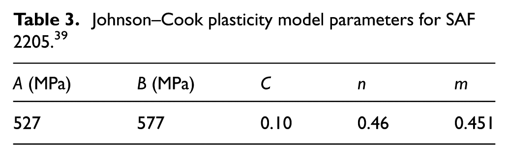
The Johnson and Cook
38
material model, equation (7), includes

Values of the Johnson–Cook plasticity model parameters were based on the work presented by Chandrasekaran et al. 39 (Table 3). An updated Lagrangian formulation was used to model the chip formation process. The cutting process was simulated using a fully coupled thermo-mechanical analysis of a two-dimensional model in ABAQUS/Standard v6.12-3. The side length of the elements in the deformation zones and at the contact interface was a maximum of 1 µm, to resolve the location of the stagnation zone.
Johnson–Cook plasticity model parameters for SAF 2205. 39
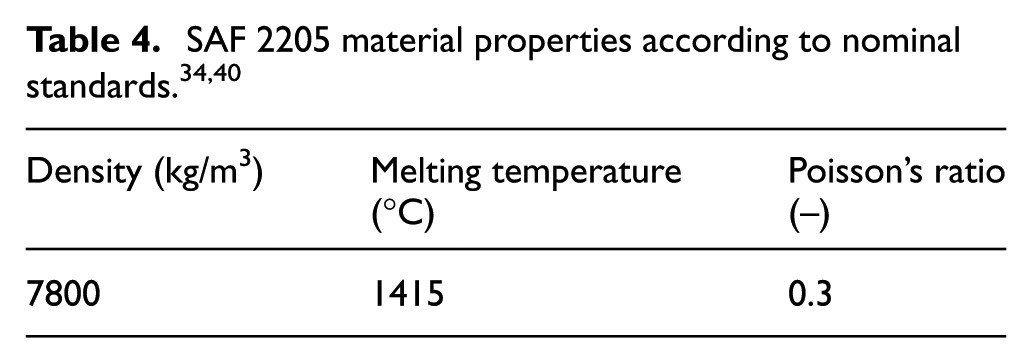
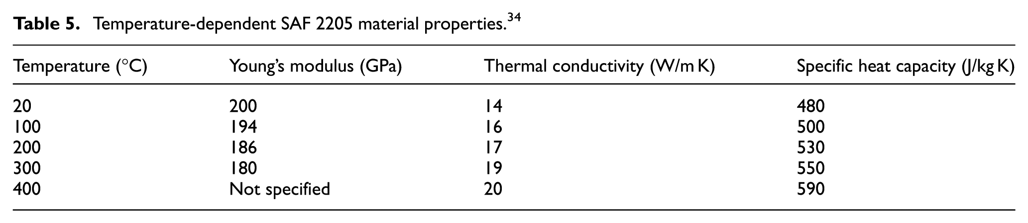
As part of the numerical investigation, the workpiece material properties stated in Table 4 were used in addition to those previously stated in Table 1. Also, as the model in some cases requires input of the temperature-dependent material properties, the values in Tables 5 and 6 were used.
Temperature-dependent SAF 2205 material properties. 34
Temperature-dependent thermal expansion of SAF 2205, mean values in temperature ranges. 34

Cemented carbide cutting tool with a rake angle of γ = 4° and clearance angle α = 6° was used. Three different tool edge radii were simulated: 40, 60 and 80 μm. The theoretical chip thickness was varied within the range of 0.001–0.40 mm to gain a broad indication of the process behavior, especially at low values of h1. The cemented carbide tool material assigned properties as summarized in Table 7.
Cemented carbide cutting tool material properties. 41
Based on the work by Bonnet et al., 42 the friction coefficient was selected at 0.27 at the tool/workpiece boundary. Furthermore, Umbrello et al. 43 state a pressure-dependent conductive heat transfer coefficient of 1000 kW/m2 K between the tool and workpiece material.
Result and discussions
Influence of process parameters on h1min
Figure 8 illustrates the different h1min values measured for the three materials included in this study: LDX 2101, SAF 2205 and SAF 2507. Consistently, it can be observed that h1min in our machining cases is significantly larger than the values reported by previous studies,14,15,18 roughly 10–30 µm. This can be either attributed to simplification of earlier analytical models, or to the specifics of machining highly ductile DSS grades in current study. In general, it was found that h1min increases with increasing h1. The presumed mechanism for such behavior is the values and direction of the forces acting on the workpiece during the cutting process. Due to an identical h1min behavior for all three DSS grades, further investigation was focusing on SAF 2205.
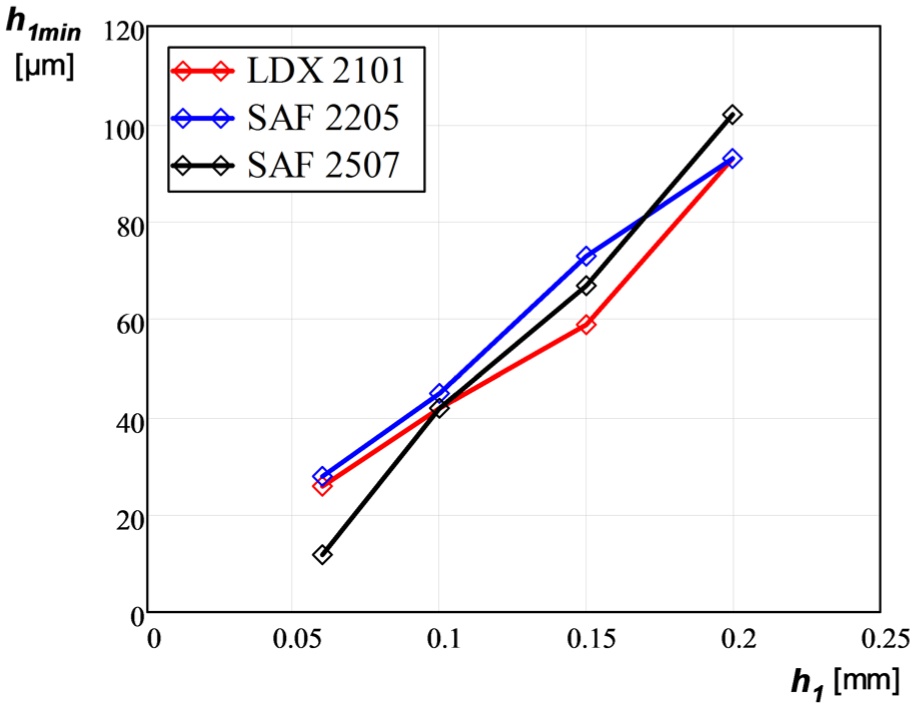
Measured h1min values in longitudinal turning three workpiece materials at vc = 125 m/min and ap = 3 mm.
The above experiments were performed for tools with edge radius rβ of 45 µm. Additional experiments with varying edge radii rβ were also conducted to investigate its influence on h1min. Surprisingly, no direct correlation between rβ and h1min was found (Figure 9), contradicting previous research.13,14,26,44
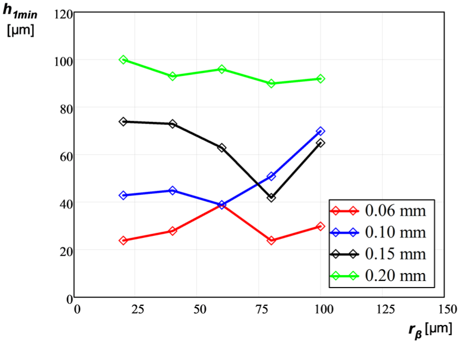
Measured h1min as a function of rβ and chip thickness h1 while turning SAF 2205, vc = 125 m/min and ap = 3 mm.
An additional array of experiments investigated the effects of tool nose radius rε. Figure 10 illustrates measured values of h1min as a function of the tool nose radius rε while machining SAF 2205. The results seem to imply, as expected, that the tool nose radii have a minor influence on the size of h1min. The effect of the nose radii is then in redistribution of the uncut material by changing the position of h1min along the edge δh1min, Figure 2, engaging larger portion of the cutting edge in the plowing action as the nose radius increases. It might be expected that if the material to be plowed has the flow direction different from the original chip flow direction, it will experience an additional deformation. In our case, chip flow angle for κ = 95° will be νch = −5° along the straight portion of the edge. However, the chip flow on the tool tip where κ = 0° will be νch = 90°; thus, this chip element has to change the direction by 95° to flow with the main chip. This is energetically unfavorable and might promote undesired flow separation and increased h1min.
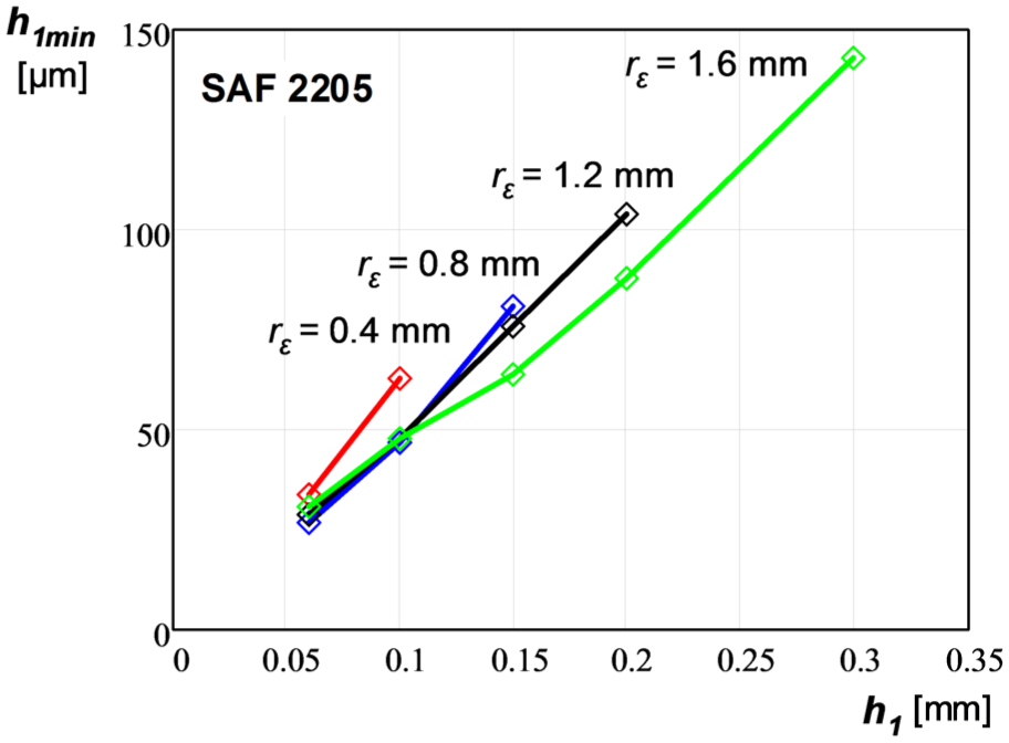
Measured h1min as a function of h1 while turning SAF 2205 with varying tool nose radii, vc = 125 m/min and ap = 3 mm.
Analysis of local chip flow angle at the point of h1min was carried out to investigate this effect. Through using equation (4) for calculating the local chip flow angle νch at the position of h1min, the following result was obtained, Figure 11. As can be seen in the figure, the material flow process changes drastically at νch ≈ 70°, indicating the existence of a threshold value after which the chip flow direction will have a significant influence on the size of h1min.
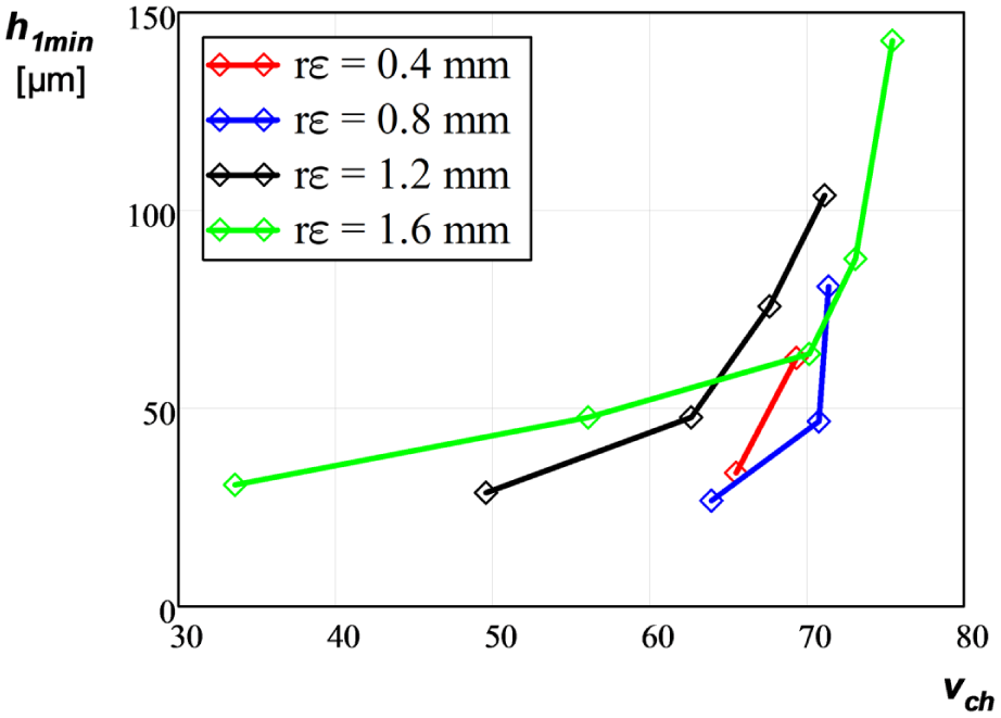
Minimum chip thickness, h1min, as a function of the chip flow angle, νch.
By analyzing Figure 11, a relationship between h1min and νch can be drawn, principally illustrated in Figure 12. Below a certain critical value of νch, the size of h1min could be considered as independent of the chip flow angle. However, when νch obtains a value that is larger than the critical value, h1min will become dependent on the size of νch, possibly concealing the correlation with rβ due to the difference in order of magnitude.
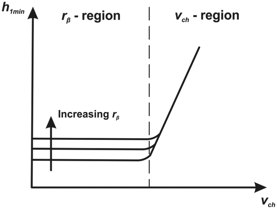
Presumed relationship between h1min and the chip flow angle νch when turning with a tool with a nose radius.
Material flow at the nose radius
To verify and further expand on the obtained results, a series of quick-stop experiments were performed as part of this investigation. During a quick-stop experiment, the cutting tool is rapidly shot away from the cutting process leaving a frozen process with the chip still attached to the workpiece which can be analyzed at a later stage. An example of the obtained result from this analysis can be found in Figure 13 which shows a view of the cutting process as seen from the reference plane. A distinct feature in Figure 13 is the material separation at the tool nose radius in addition to the primary deformation zone (Zone I), secondary deformation zone (Zone II) and tertiary deformation zone (Zone III). It is also possible to distinguish a chip side flow, based on the observed material deformation pattern, in which the chip is plastically deformed after it has been cut.
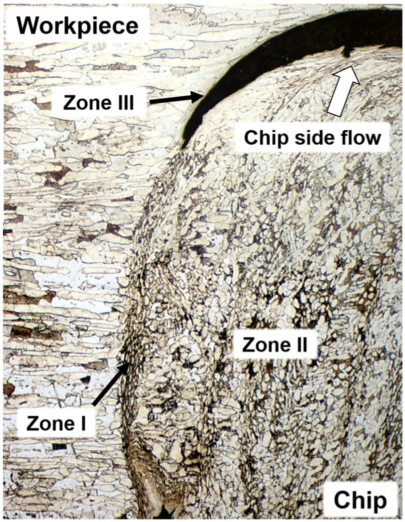
Material flow at the tool nose radius as seen from the reference plane. 19
Numerical results
An illustration of the stagnation zone formed at the contact interface is presented in Figure 14, with an edge radius of 40 µm and a theoretical chip thickness of 0.05 mm.
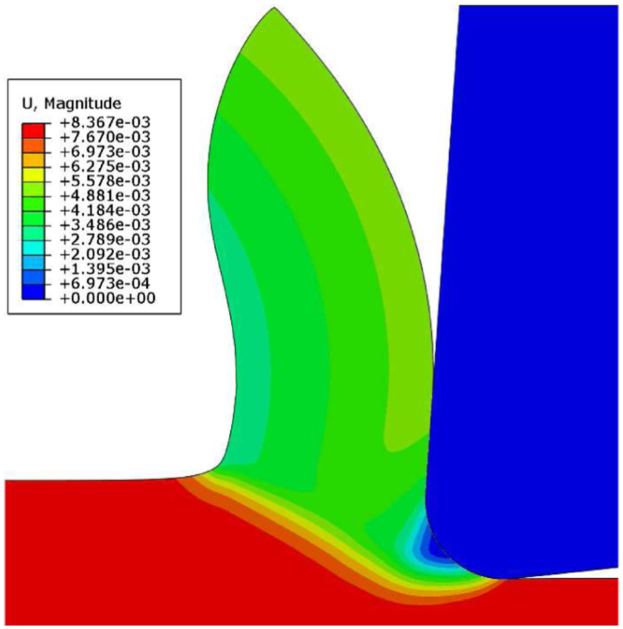
Magnitude of nodal displacements in the workpiece within a remeshing interval.
Based on the notion that the shear force acting along the perimeter of the tool edge radius will change direction when passing the stagnation zone, the location of the stagnation point and thus the size of h1min can be established as a function of the angular position (Figure 1). Figure 15 illustrates the vertical shear force acting on the cutting tool as a function of the angular position θ for low values of h1. In Figure 15, only h1 = 0.004 and 0.010 mm displays a behavior indicative of the creation of chips through the existence of a stagnation zone and thus a minimum chip thickness. This is due to the clear change in shear force direction while moving along the angular position on the tool edge radius indicative of a stagnation point.
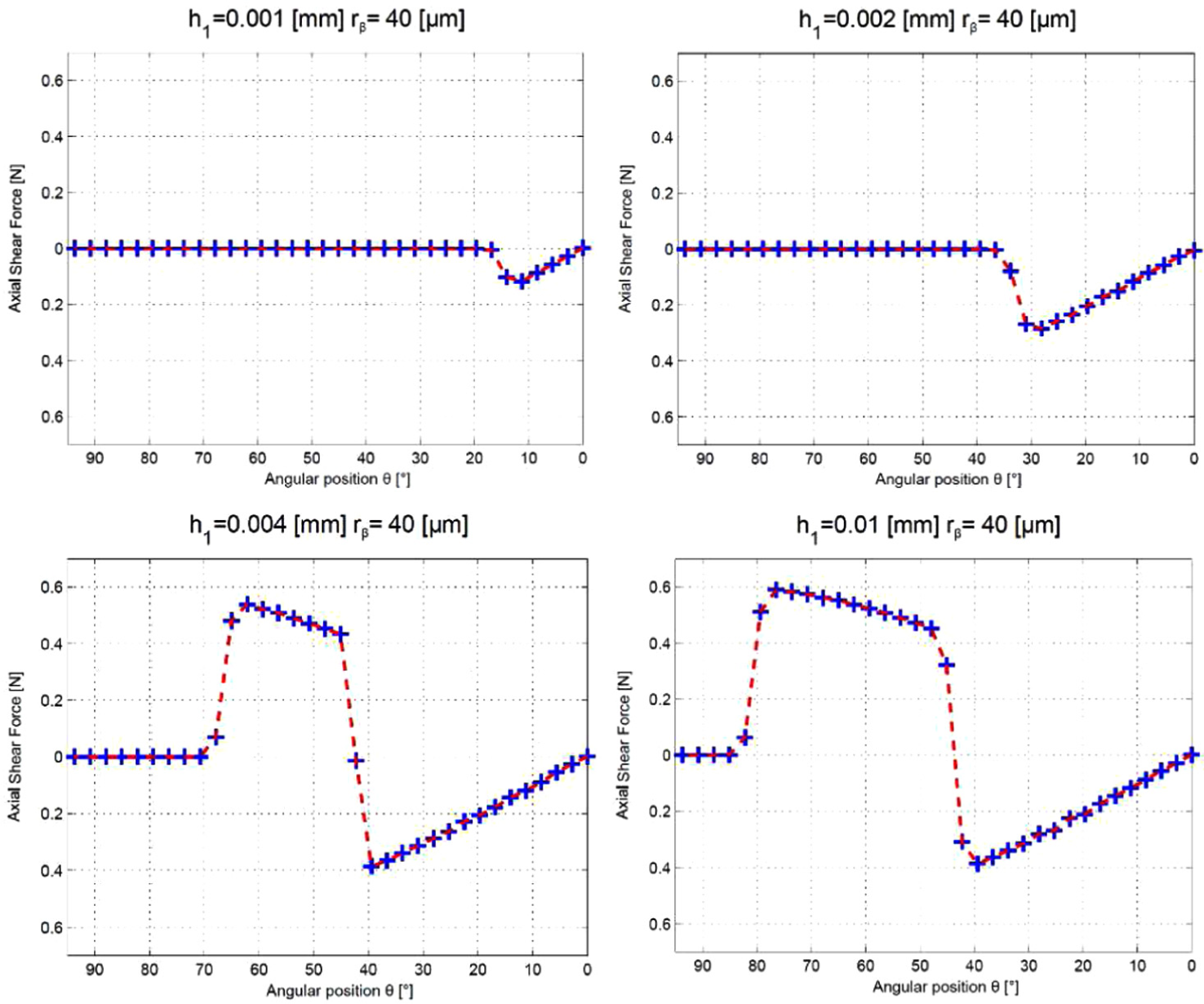
Axial shear forces acting on the cutting tool in the tool/workpiece contact as a function of the angular position θ.
Through analysis of this type of results, a relation between the stagnation angle and theoretical chip thickness was established, Figure 16. As can be seen in the figure, the development of the stagnation angle as a function of the theoretical chip thickness appears to follow the same trend for all tool edge radii investigated. However, any clear relation between the size of the tool edge radius and the stagnation angle is once again difficult to distinguish. Worth noting is that these values for the stagnation angle coincide well with previously reported results.14,15,18 If comparing with the calculated cutting forces, Figure 17, it can be argued that the near-linear growth of θs after h1 = 0.05 mm is the cause for the stabilization of the feed force Ff after h1 = 0.05 mm, that is, the feed force becoming linearly dependent on the theoretical chips thickness.
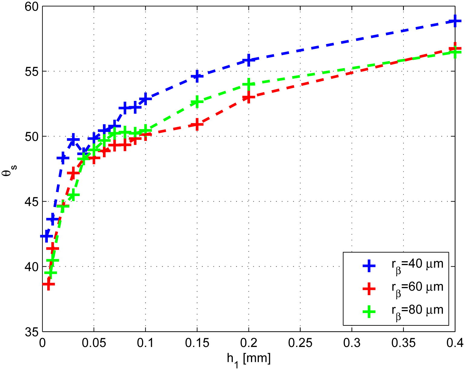
Stagnation angle θs as a function of h1 for varying tool edge radii rβ.
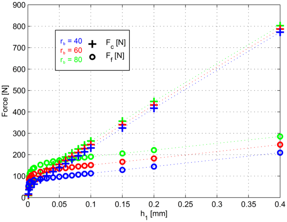
Main cutting force, Fc, and feed force, Ff, as a function of h1 for varying tool edge radii rβ.
Discussion
The developed method adequately captures the effect of varying process conditions on the size of h1min. The being measured fraction of the tool contact length that is engaged in chip formation, when compared to the theoretical length, provides the length of the cutting edge engaged in a plowing action, thus quantifying h1min. Accurate measurements of chip width were found to correspond to the tool contact length measured with microscopy. Worth noting that the experimentally measured values of h1min are significantly larger than previously published analytical values.14,15,18 This can be related to the influence of the machining operations being investigated. Earlier studies14,15,18 focused on orthogonal cases where h1min defines a fraction of h1 that does not participate in chip formation. Application of the same definition onto a realistic longitudinal turning with tooling having a nose radius quantifies the amount of uncut material that remains on the workpiece and affects surface quality and integrity. A more complex material separation behavior encountered in longitudinal operation, as compared to the simplified analytical models of orthogonal cases, accounts for effects such as stagnation zone, chip flow, material ductility. Therefore, current values of h1min, accounting for the full range of effects, exceed values reported for stagnation zone only. At the same time, our numerical FEM data for the stagnation angle coincide well with previously reported results.14,15,18
Conclusion
In this study, a novel approach for experimentally measuring h1min was developed. The implemented measurement method adequately depicts the effect of varying process conditions on the size of h1min. The method and associated analytic solutions are only valid for machining case A (Figure 3), imposing restrictions on the feed, nose radius and minor cutting edge angle (equation (1)).
The main conclusions from this study are as follows:
The size of h1min shows a linear relationship with the theoretical chip thickness h1 where h1min can reach up to 40% of h1.
Experimentally measured values of h1min are larger than previously published analytical values, which is related to an investigation of longitudinal turning as opposed to simplified orthogonal.
A relationship between rβ and h1min cannot be distinguished in the experimental nor numerical results, contrary to previous research.
A clear relationship between h1min and the tool nose radii rε was observed where a decreasing size of the tool nose radius leads to increased h1min.
A local chip flow angle νch was found to describe the loads acting on the chip at the location of the stagnation point and thus h1min.
Footnotes
Appendix 1
Acknowledgements
The authors wish to acknowledge the contribution made by Seco Tools and particularly express their gratitude toward Bengt Högrelius for the assistance provided.
Declaration of conflicting interests
The author(s) declared no potential conflicts of interest with respect to the research, authorship and/or publication of this article.
Funding
The author(s) disclosed receipt of the following financial support for the research, authorship, and/or publication of this article: This work has in part been done within the ShortCut research project funded by the Swedish Foundation for Strategic Research. The research is also part of the Sustainable Production Initiative SPI; a cooperation between Chalmers and Lund University.