
Abstract
The machining of a CaF2 lens with the near-perfect crystal structure poses a more challenging task than simply performing a ductile-regime cutting on brittle materials to achieve an optical surface finish without microcracks in the subsurface layer. This research advances the understanding of the ductile–brittle transition mechanism through material characterisation. The convincing evidence for the advantage of ultraprecision diamond turning over the optical polishing process is disclosed in the comparative experimental tests. A promising solution of thermally enhanced microcutting is proposed to meet both the ubiquitous and ad hoc requirements for the fabrication of the CaF2 lens. The theoretical foundation for the CaF2 microcutting at elevated temperatures is for the first time established based on a semi-quantitative modelling and simulation with the crystal plasticity finite element method.
Keywords
Introduction
Single-crystal calcium fluoride (CaF2) stands out with its identity as a superior optical material owing to its high Abbe number and wide transmission range. Differing from the conventional optical requirements on a complex structured and functional surface, the 193-nm immersion lithography prescribes an evermore stringent demand on extremely low refractive index inhomogeneity for CaF2 lenses of above 200 mm diameter and 50 mm thickness. 1 The high index homogeneity relies not only on the grade of CaF2 crystals but also on the strict control of the crystal structural defects induced by the processing factors.
The state-of-the-art research on ductile-regime cutting of brittle materials seeks solutions to several critical problems including the following: (1) crack formation and subsurface damage;2,3 (2) determination of critical undeformed chip thickness 4 using different experimental techniques such as plunge cutting, 5 fly cutting, 6 scratching, 7 and diamond turning; 8 (3) theoretical solutions through modelling and simulation using analytical model, 9 molecular dynamics simulation,3,9 and finite element method; 8 (4) material anisotropy effect on machining;8–10 and (5) machining-induced amorphous layer such as in single-crystal Si and SiC.11,12 Although ductile cutting of various brittle materials can be achieved under properly adjusted machining parameters, the unsolved problem of subsurface damages, such as the formation of an amorphous layer in Si/SiC and microstructural changes in CaF2, 8 is still observable to affect the optical properties of the final product.
Hybrid or assisted machining technology applies multiple machining processes simultaneously preferably with the combined energy assistance to remedy the potential disadvantages of individual material removal processes. An up-to-date review on this topic was contributed by Unune and Mali. 13 As a representative process in the category of the assisted machining technologies, laser-assisted machining has been developed to enhance the machinability of high-strength materials such as steel, titanium alloys, ceramics, and composites14–16 by the softening effect by different heat sources. This article explores the feasibility of applying laser-assisted machining techniques to CaF2 microcutting. The theoretical foundation for the CaF2 deformation at elevated temperatures is established based on a semi-quantitative modelling and simulation with the crystal plasticity finite element method (CPFEM).
Problem statement from the experimental study
The microcutting experiments were performed on the (111) CaF2 single crystals at the room temperature. The experiments aimed to uncover the anisotropic effect of CaF2 single crystals on ductile–brittle transition (DBT), surface generation, and subsurface integrity. Different material characterisation techniques were adopted to identify the existing problems of the process-induced crystallographic defects in the subsurface which negatively affects the optical homogeneity of the CaF2 component. The experiments, as a starting point, motivated this study of the theoretical foundation for the thermally assisted microcutting of CaF2 single crystals.
Infrared optical-grade (111) CaF2 workpieces of 8 mm diameter were indexed by the
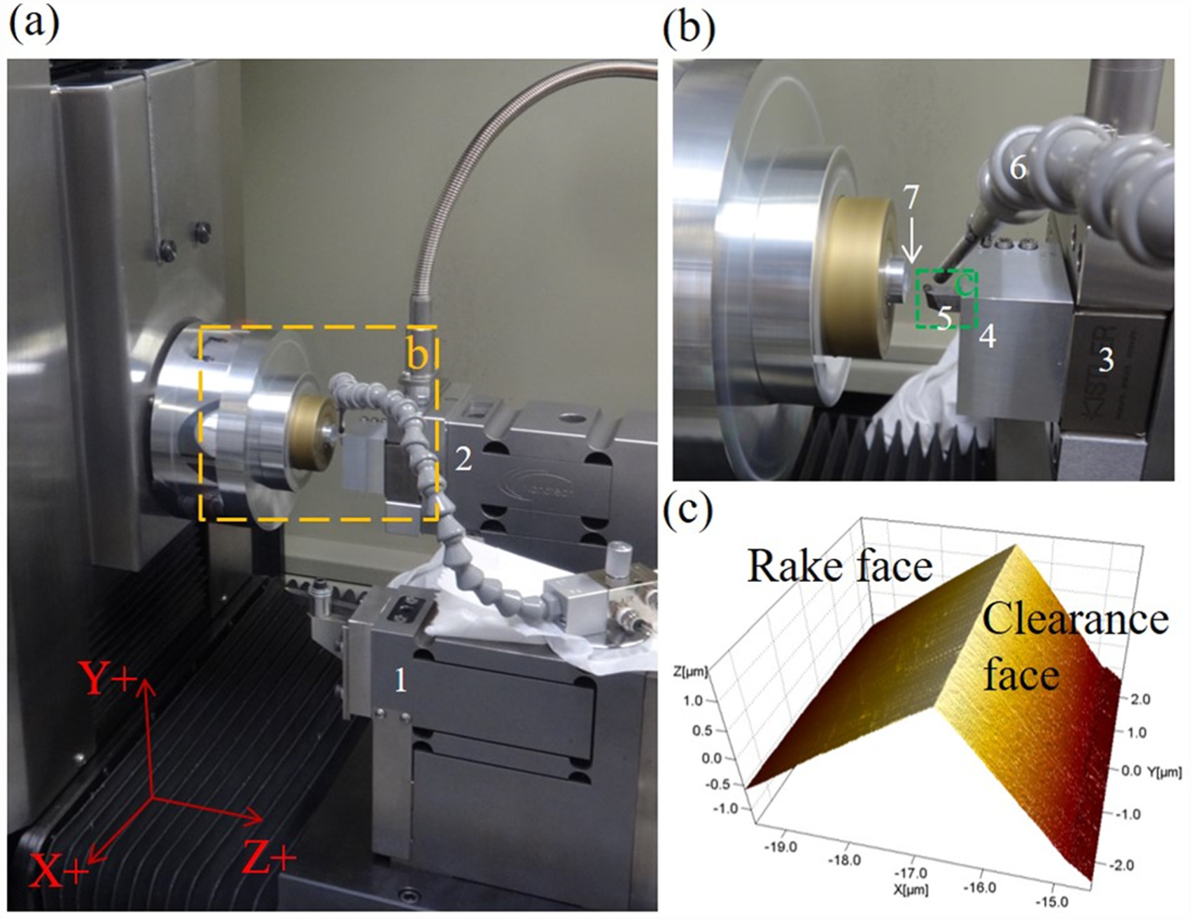
(a) Experimental set-up on Nanotech 350FG machine with (b) a close-up of the CaF2 sample and diamond tool for plunge cutting, and (c) an AFM micrograph of the cutting edge profile (left: rake face; right: clearance face). (1: tool post for pre-machining; 2: tool post for plunge cutting; 3: Kistler dynamometer; 4: tool holder; 5: a diamond tool for plunge cutting test; 6: spray mist supply (used in pre-machining only); and 7: CaF2 workpiece).
To ensure the reliability of the subsequent plunge-cut tests, the CaF2 sample surfaces were first prepared by a rough-cut process with a spindle speed of 700 r/min, a feed rate of 8 mm/min, and a depth of cut of 1 µm with an SCD tool of 1 mm radius, −25° rake angle, and 9° clearance angle. The sample surface was finished with a reduced feed rate of 3.4 mm/min and paraffin oil to improve the surface finish. A Talysurf CCI white light interferometer (WLI) qualified the pre-machined surface by an arithmetic mean height (Sa) of 1.832 nm (Figure 2(a)). A Horiba XploRA microscope verified the Raman spectrum signatures of the as-polished sample (labelled as ‘As-polished’ in Figure 2(b)) and the pre-machined surface equally sampled at every 15° starting from the
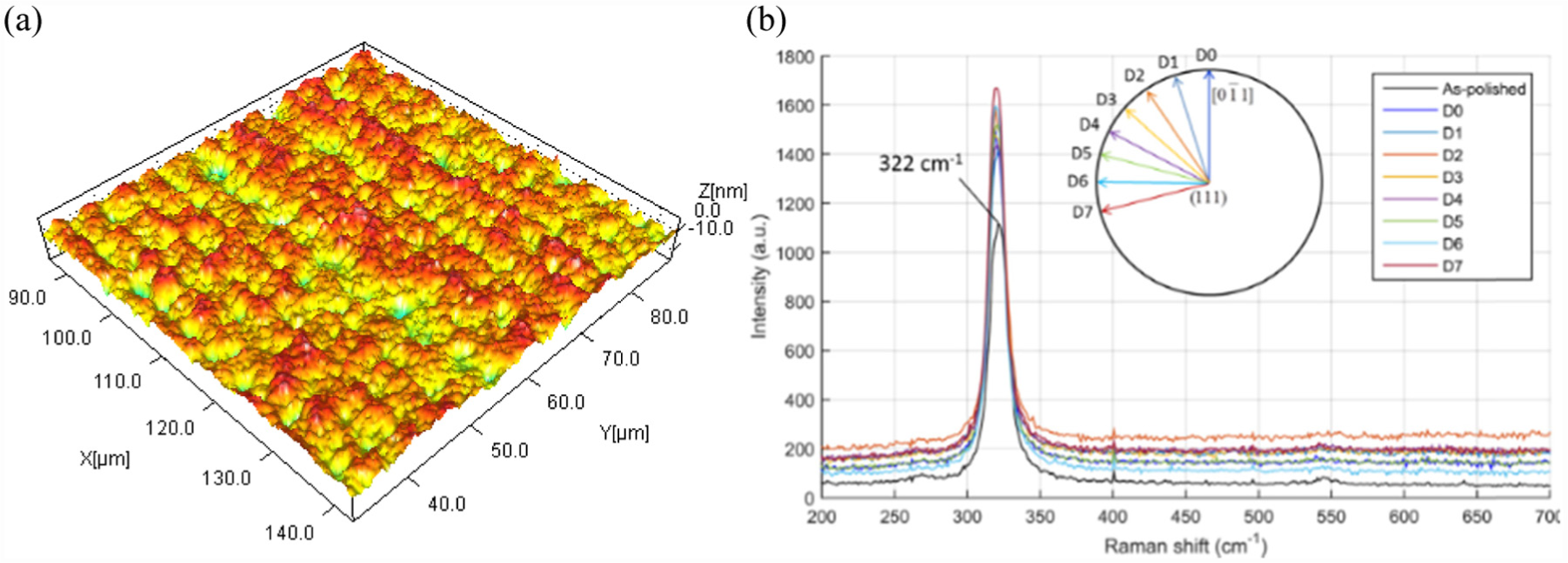
(a) Measured profile of the pre-machined surface using WLI and (b) Raman spectra of the as-polished sample and the pre-machined surface (D0–D7 denote the eight crystallographic directions with a 15° angular increment from
Chemical etching method was proven to be effective and less time-consuming to reveal the lattice imperfection and dislocation distributions based on the variation of the frontal (vF) and lateral (vL) etch speed. Motzer and Reichling 17 observed the ditrigonal etch pits (Figure 3(a)) on the cleaved surface of the (111) CaF2 after etching with hydrochloric acid (HCl). The frontal etch speeds were 13 and 54 nm/min, and the lateral etch speeds were 140 and 680 nm/min with the HCl concentrations of 2 and 12.4 M, respectively. In this work, the etching was performed with 37% HCl for 15 min. The maximum etch pit depth was approaching to 810 nm at dislocation sites, while a layer of about 80 nm from the initial surface was etched away, as shown in Figure 3(b). The WLI images of the as-polished surface and the diamond-turned surface after etching, as shown in Figure 4, suggest a more uniform subsurface prepared by diamond turning. Trains of etch pits associated with the hidden dislocation network of the as-polished sample would deteriorate the index homogeneity, although the polishing method prepared an atomic-level surface roughness (Ra) of 0.81 nm and a maximum height of the profile (Rt) of 10.48 nm over a sample area of 840 µm × 840 µm. Thus, a critical technical problem is raised from such an observation – a seemingly excellent surface finish does not guarantee the perfect subsurface integrity or optical homogeneity.
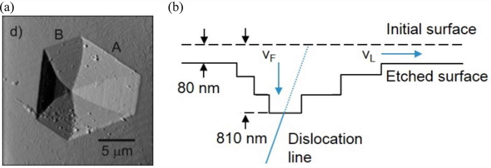
(a) Ditrigonal etch pit on CaF2 (111) 17 and (b) the etch depth and pit formation with 37% HCl for 15 min.
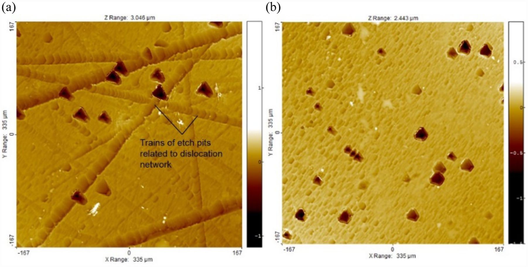
WLI images of (a) the optical-polished surface showing trains of etch pits after etching and (b) the diamond-turned surface showing the signature of scattered etch pits after etching.
Plunge-cut tests in a dry-cutting condition were further performed following the orientation notation used in Figure 2(b) with a fixed plunge angle of 0.036° and a cutting speed of 50 mm/min. The orientation-dependent DBT and different surface morphologies can be observed in Figure 5. A detailed discussion about the DBT, surface generation, cutting force, and crack morphology refers to our prior work. 8 Since the minimum critical undeformed chip thickness is approximately 30 nm, taking account of all orientations, the ductile-regime cutting condition can be readily met by setting up an appropriate combination of machining parameters for spindle speed and feed rate. However, the high-resolution cross-sectional transmission electron microscopy (HR-TEM) images (Figure 6) of the subsurface layer in the ductile-cut region along the D0 direction, as indicated by the blue arrow in Figure 5, revealed some unseen problems of severe lattice rotation, dislocations, nanocrystal formation, and so on. These problems, to some certain extent, were caused by the microcutting-induced stress field associated with the brittle nature of CaF2, which hinders the plastic deformation. Therefore, an enhancement of the dislocation activities, as a remedy, could be expected by applying a thermal field. The theoretical foundation will be elucidated in the next section.
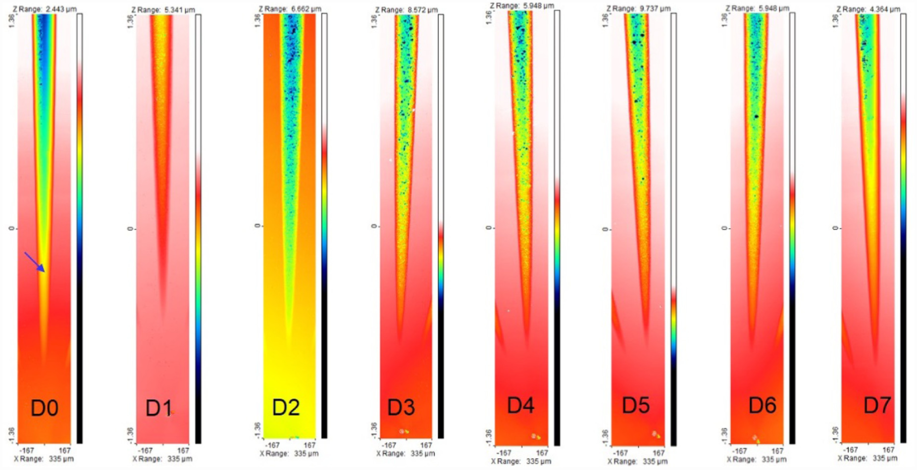
WLI images of plunge-cut profiles in different crystallographic directions (the blue arrow in D0 denotes the lift-out sample site for the HR-TEM investigation).
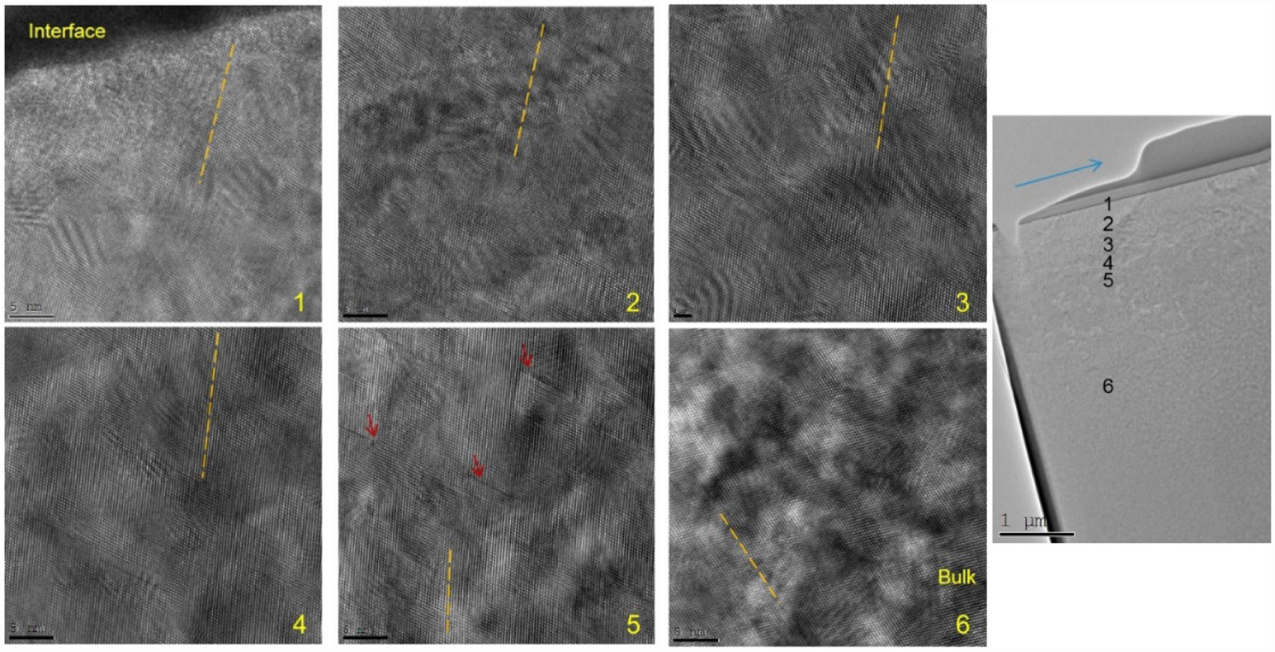
HR-TEM images to reveal the room-temperature microcutting-induced crystal defects in the subsurface: (1) from the machined surface to (6) the intact bulk material (the blue arrow indicates the cutting direction).
Theoretical analysis
A CPFEM simulation for the orthogonal microcutting was developed to semi-quantitatively establish the theoretical foundation through differentiating the dislocation behaviours and the cutting force predictions for the material removal processes at the room and elevated temperatures. In this work, a simplified CPFEM model aims to qualitatively reflect the thermal effect on the microcutting process through a semi-quantitative set-up of the numbers of the activated slip systems at the room temperature, 200 °C and 400 °C, based on the experimental observation reported by Muñoz et al., 18 rather than using a conventional calibration for the temperature-dependent parameters in the crystal plasticity constitutive model.
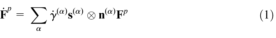
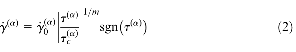
The CPFEM modelling follows our prior work 8 using ABAQUS/Standard. A total of 28,336 C3D8R elements were used to model the CaF2 workpiece subject to the pre-defined tool–work contact condition. The diamond tool was represented by a rigid analytical surface. This simulation was performed at a depth of cut of 0.1 µm, cutting speed of 50 mm/min, and along the crystallographic direction D0 before the onset of microcrack initiation and propagation. The crystal plasticity constitutive equations governed by Schmid’s law, as expressed in equations (1)–(4), were integrated to the simulation with ABAQUS/Standard through the UMAT subroutine 8
The anisotropic plastic deformation of CaF2 is dominated by slip systems of {100}<110> at the room temperature. The elastic stiffness constants C11, C12, and C44 were 168.16, 48.54, and 33.81 GPa, respectively.
To evaluate the thermal effect on the dislocation activities in the ductile-regime microcutting of CaF2, the cumulative shear strains on all the slip systems for the room temperature (with one activated slip system), 200 °C (with two activated slip systems), and 400 °C (with three activated slip systems) are compared in Figure 7. In view of the material anisotropy, both side views of the simulation results are plotted. The simulated results confirm not only the enhanced plastic deformation due to the dislocation activities but also a transition from the asymmetric deformation and ductile–brittle transition (aDBT) 8 in case 1 to a more symmetric state in cases 2 and 3. The simulated lateral cutting force, as shown in Figure 8(a), also presents a more balanced force (a reduced force level means approaching to the equilibrium state). This could also be an advantage of the thermally enhanced microcutting for producing a homogeneous surface finish. In the meantime, the cutting force and thrust force are both reduced by about 50%. Thus, the enhanced ductility plus a reduced stress level will favour the ductile-regime cutting and reduce the subsurface damage and the probability to induce crystal defects as well.
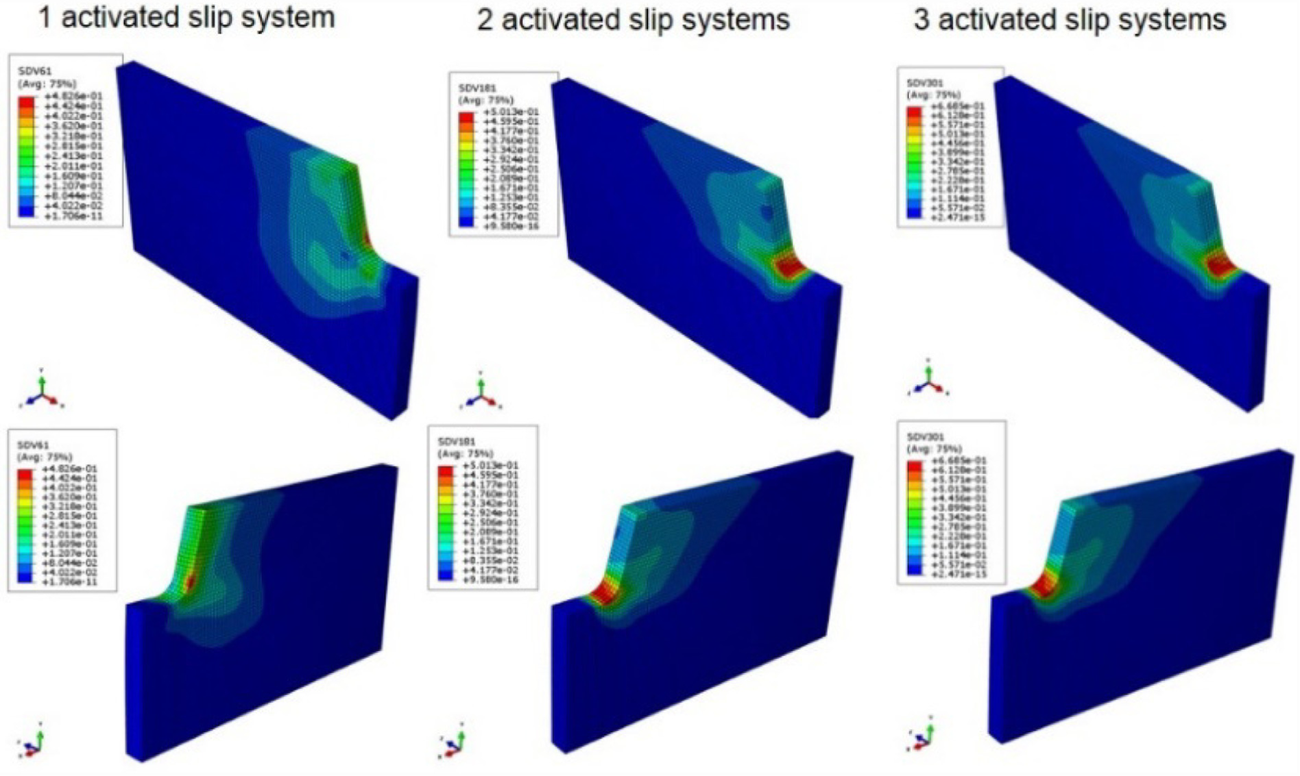
Simulated cumulative shear strains on all the slip systems subject to the ductile-regime orthogonal cutting for one (25 °C), two (200 °C), and three (400 °C) activated slip systems.
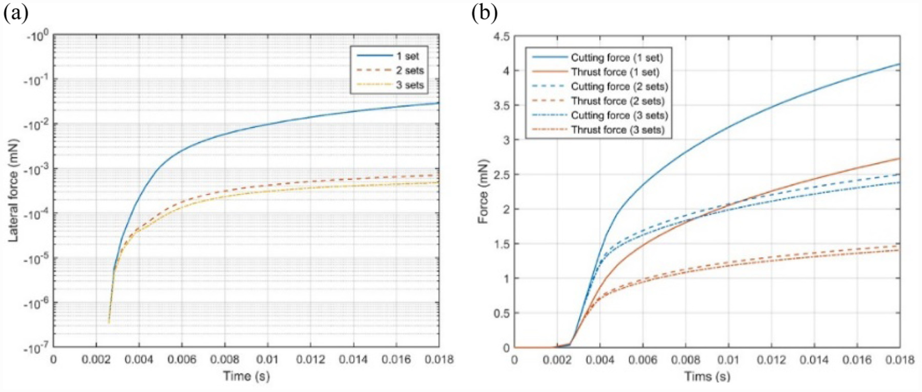
Simulation results of (a) the lateral force and (b) the cutting and thrust forces.
Summary
This article develops a new understanding of the ultraprecision diamond turning and optical polishing of CaF2 single crystals by comparing the morphology and aggregation of the etch pits. The critical factors regarding the fabrication of a near-perfect CaF2 lens are identified with the promising solution of thermally enhanced microcutting. The theoretical foundation for the CaF2 microcutting at elevated temperatures is therefore established based on a semi-quantitative simulation with the CPFEM. This article states the problems and researches the methodology and feasibility of applying the thermally assisted machining technique to CaF2 crystals. This theoretical work is a generic discussion and sets no constraints to the heat source selection or heating methods for the future experimental work.
Footnotes
Appendix 1
Declaration of conflicting interests
The author(s) declared no potential conflicts of interest with respect to the research, authorship, and/or publication of this article.
Funding
The author(s) disclosed receipt of the following financial support for the research, authorship, and/or publication of this article: This work was supported by the Ministry of Education, Singapore; National University of Singapore; and Alexander von Humboldt Foundation.