
Abstract
Material characteristics, such as electric potential, distance between target material and substrate, and so on, are important parameters for vacuum metal films deposition (sputtering) system. Properly controlling these parameters during the sputtering process can reduce the residual stress after deposition and can effectively improve the deformation of substrate and density of metal thin film. This study aims at simulating a vacuum metal film deposition system for substrate application with normal metal material. Both the copper foil, as a target material, and the substrate that is placed on a carrier platform are included in a vacuum chamber. The argon ion gas is excited by a radio frequency power generator to form the plasma source in the sputtering system. “Glow Discharge” of the “Paschen Curve” during plasma generation process is employed to excite the argon ion gas to bombard the target material. The ejected atoms of target material are deposited on the substrate surface to form the desired thin films. Several different parameters, such as radio frequency power, electric field intensity, distance between the target materials and the substrate, and so on, are discussed in this article. Numerical analysis results indicate that the distance between the substrate and target materials may affect the density of metal film significantly. The MATLAB simulation results can provide the technique of finding better workpiece height and high coating quality for the semi-conduction industrial adopting sputtering system for metal thin film production.
Introduction
Plasma technology is frequently applied in the aerospace engineering industry, polymer industry, and environmental pollution control, such as coating optical components, tool life improvement of anti-wear film, non-woven optical plastic or glass surface treatment, micro-sensor manufacturing, micro-mechanical machining, anti-wear coating of artificial joints and organs, and surface treatment of biomedical materials. Therefore, plasma technology provides considerable impact to the development of these industries.
Integrated circuit (IC) logic chips are currently in 28-nm process for mass production, and 14-nm technology has been started to manufacture by the Taiwan Semiconductor Manufacturing Company (TSMC) since 2015. In order to meet the demand of increasingly fine groove width and larger depth, good variety of film material with thinner, better growth, and filling characteristics has to be established. Accordingly, more precision coating technology has been developed:1–3 from early physical vacuum deposition 4 (vacuum evaporation), conventional magnetron sputtering, 5 to state-of-the-art high-density plasma ion-beam sputtering. 6
Lo 7 builds up an inductively coupled plasma ion-beam sputtering deposition (ICP-IBS) system for the fabrication of microelectronic thin films. Then, the fabrication of copper and copper–titanium alloying thin film was followed up after complete understanding of the characteristics of the ICP-IBS system. The resistivity of as-deposited copper thin films was about 4 µΩ cm and was reduced to ∼2 µΩ cm after vacuum thermal processing at 500 °C for 4 h. Hong 8 studies the effects of the plasma surface treatments and the sputtering operating conditions on the adhesion properties, and the durability of the polyimide (PI)/metal interface is studied with atomic force microscopy (AFM), attenuated total reflection infrared spectroscopy (ATR), contact angle measurement, and peel strength measurement. Investigations by Zhang and Chou 9 use the finite element analysis to model the part distortions in fused deposition. This research investigates the electrical potential and electric intensity of a vacuum metal film sputtering system with distance effect between the substrate and target material by MATLAB numerical simulation software.
Simulation
Vacuum metal film sputtering system diagram is described in Figure 1. Both the copper foil (target material), excited by a maximum 500 W radio frequency (RF) power generator, and the silicone substrate (placed on a carrier platform) are placed in a 2 × 10⁻⁵ torr vacuum chamber. Argon ion gas is input to bombard the copper foil target material. The imported argon ion gas is excited by a RF power generator to form the plasma source in the sputtering system. “Glow Discharge” of the “Paschen Curve” during plasma generation process is employed to excite the argon ion gas to bombard the target material. The ejected atoms of target material are deposited on the substrate surface to form the desired thin films.
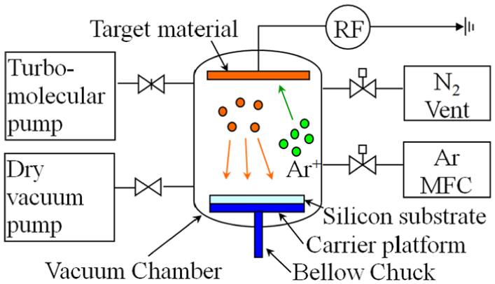
Vacuum metal film sputtering system diagram.
Based on the characteristics of the electromagnetic system, Laplace equation and Poisson equation are only suitable for describing the static and low-frequency operating conditions. In the high-frequency applications, one or more solutions of the partial differential equations with proper boundary conditions must be solved in time or frequency domain in order to accurately predict electric and magnetic fields. Finite difference method (FDM) is employed to discretize the solution domain into meshes and nodes. The field of partial differential equations is transformed into the electrical and magnetic potential of each node of difference (algebraic) equations with unknown coefficients. The numerical solution of electric potential or electric intensity of the metal film sputtering system can be obtained by MATLAB numerical simulation software and solving these equations of the discrete nodes. MATLAB simulation model of the metal film deposition system is shown in Figure 2.
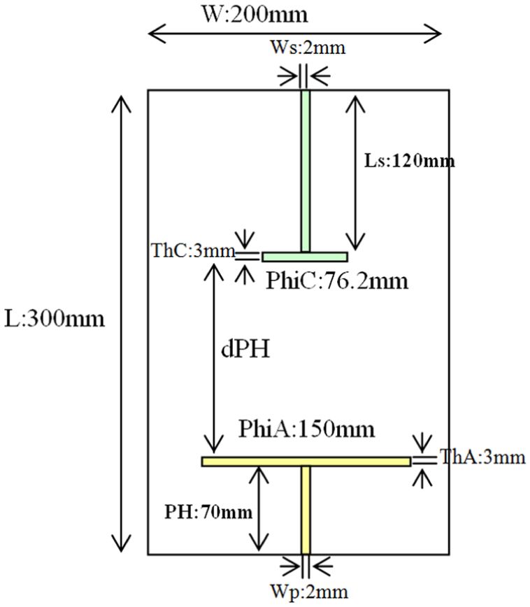
MATLAB simulation model of the Metal film deposition system.
Result and discussion
The RF power of the sputtering source is restricted to 500 W. Hence, the relationship between RF power and the average resistance value of thin-film chip is first measured to find the suitable value of RF power, as shown in Figure 3. RF power of 100 and 500 W are ruled out since the increasing trend of resistance is too large, as shown in Figure 3. Due to the small variation of resistance, RF power of 150 W is chosen for simulation. In thin-film deposition process, the distance (height) between the target material and workpiece (on carrier platform) is one of the key factors to affect the coating thickness. Different height of the workpiece and different RF power will change the RF electric field intensity as well. Therefore, finding out the location of the workpiece can effectively reduce errors in actual sputtering process. Analysis result indicates that the suitable range of workpiece position is 0–20 mm to maintain normal electric intensity. However, when the distance of the workpiece is 5 mm with RF 150 W, the simulated electric field intensity and electric equipotential are beyond the reasonable value (Figure 4). Therefore, the adjustable distance of the workpiece is re-defined to 5–20 mm.
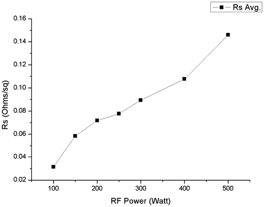
The relationship between RF power and the average resistance value of thin-film chip.
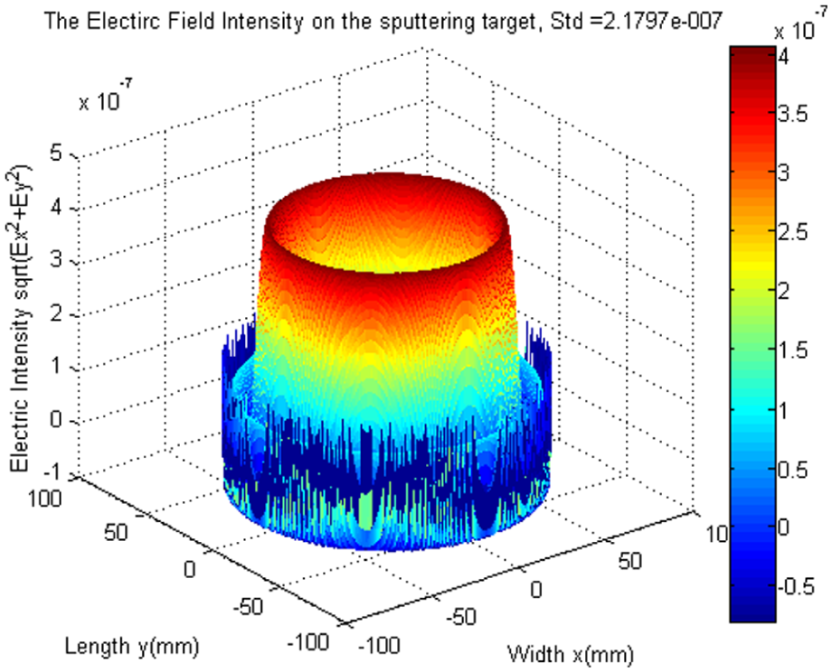
The electric field intensity on the sputtering target when the height of the workpiece is 5 mm with RF 150 W.
The simulation result of electric field intensity of different RF power with workpiece distance of 5–20 mm is shown in Figure 5. The RF power will affect the electric field intensity. Higher RF power will produce higher electric intensity. The electric field intensity is on the peak value at workpiece distance of 8 mm for each RF power. Higher or lower than 8-mm distance (height) of the workpiece maintains lower electric intensity.
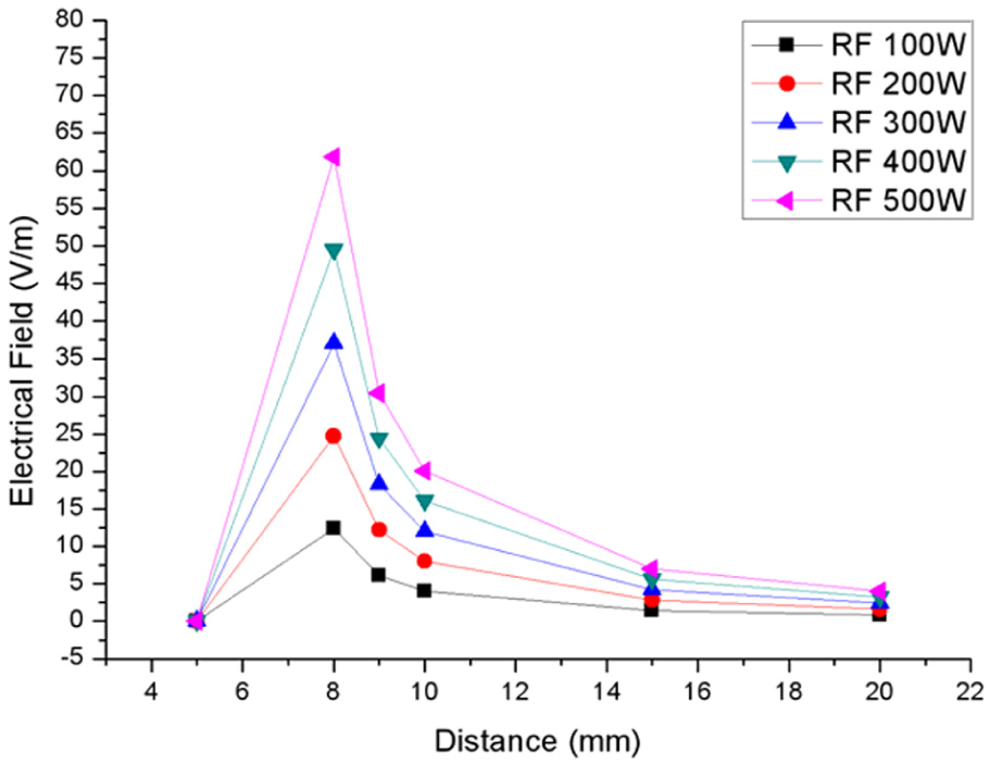
The electric field intensity of different RF power with workpiece height of 5–20 mm.
The analysis of this research is summarized as follows:
The RF power will affect the electric field intensity. Higher RF power will produce higher electric intensity. The electric field intensity is on the peak value at workpiece distance (height) of 8 mm for each RF power.
The electric intensity is increasing with the target thickness for all different heights of the workpiece. The smaller the height of the workpiece, the larger the electric intensity.
Footnotes
Declaration of Conflicting Interests
The author(s) declared no potential conflicts of interest with respect to the research, authorship, and/or publication of this article.
Funding
The author(s) received no financial support for the research, authorship, and/or publication of this article.