
Abstract
Geometric features of the segmented chip have been investigated along with the volume of material removed at a cutting speed at which tool wear is characterized by the gradual development of flank wear when cutting Ti-6Al-4V alloy. The chip geometric variables varied with an increase in the volume of material removed as the combined effect of change in tool’s geometry and increase in cutting temperature. Plastic deformation dimples were observed as periodical regions on the machined surface, a row on each undeformed surface and region on the top of the slipping surface of the segmented chip when cutting with new tool; these dimples on the undeformed surface and machined surface are elongated in the direction of chip flow. All these dimples became less with an increase in the volume of material removed and almost disappeared when the chip was removed with the worn tool at the end of its life. A model of segmented chip formation process has been proposed to satisfactorily explain the formation of the plastic deformation dimples on the undeformed surface and machined surface of the segmented chip produced with a new cutting tool and the transition of chip geometry with the evolution of tool wear.
Introduction
Mechanical machining is a material removal process which produces different types of chips due to the different deformation mechanisms at the shear zone. The chips can be classified as discontinuous chips, continuous chips, continuous chips with built-up edge and serrated chips (also known as saw-tooth or segmented chips). 1
Segmented or saw-tooth chips is the typical chip produced when machining a group of workpiece materials with high hardness and low thermal conductivity, such as titanium alloys,2–7 nickel alloys8–10 and hardened steels4,11 at different critical cutting speeds for the onset of segmentation. The critical cutting speed for the onset of chip segmentation is very low when machining titanium alloys. 12 Since segmented chip formation during cutting results in high cyclical cutting forces 13 and severe crater wear that leads to a decrease in tool life, 14 and a rough surface finish as a result of tool vibration and chatter, continuing efforts have been undertaken over many years to investigate the formation and features of segmented chips.
A typical cross section of the segmented chip made during high-speed machining of Ti-6Al-4V alloy is shown in Figure 1. Points A and F′ are the valley points of a segment on the undeformed surface side and slipping surface side, respectively, at which open cracks are normally formed; point B is the peak tip of a segment; points C and D are the intersections of shear bands with the machined surface of the chip and a periodic wavy profile with valley point E is found on the machined surface. The undeformed surface represented by line A-B is produced by the tool’s flank face in the previous revolution of the cut, and the machined surface represented by line C-D is produced by the tool’s rake face in the current revolution of cut. The slipping surface represented by line B-F′ is produced during segmentation, on which the lower part surface represented by line F-F′ shows more significant shear deformation than the upper part of line B-F′. The geometric features are characterized by shear band width,
15
the depth of the ‘saw-teeth’ (the distance each segment slides outward), segment spacing (shear band spacing, distance between shear bands), length of undeformed surface,
13
chip roughness ratio,16,17 the degree of segmentation,10,18 chip segmentation frequency, shear angle, inclination angle of a segment (
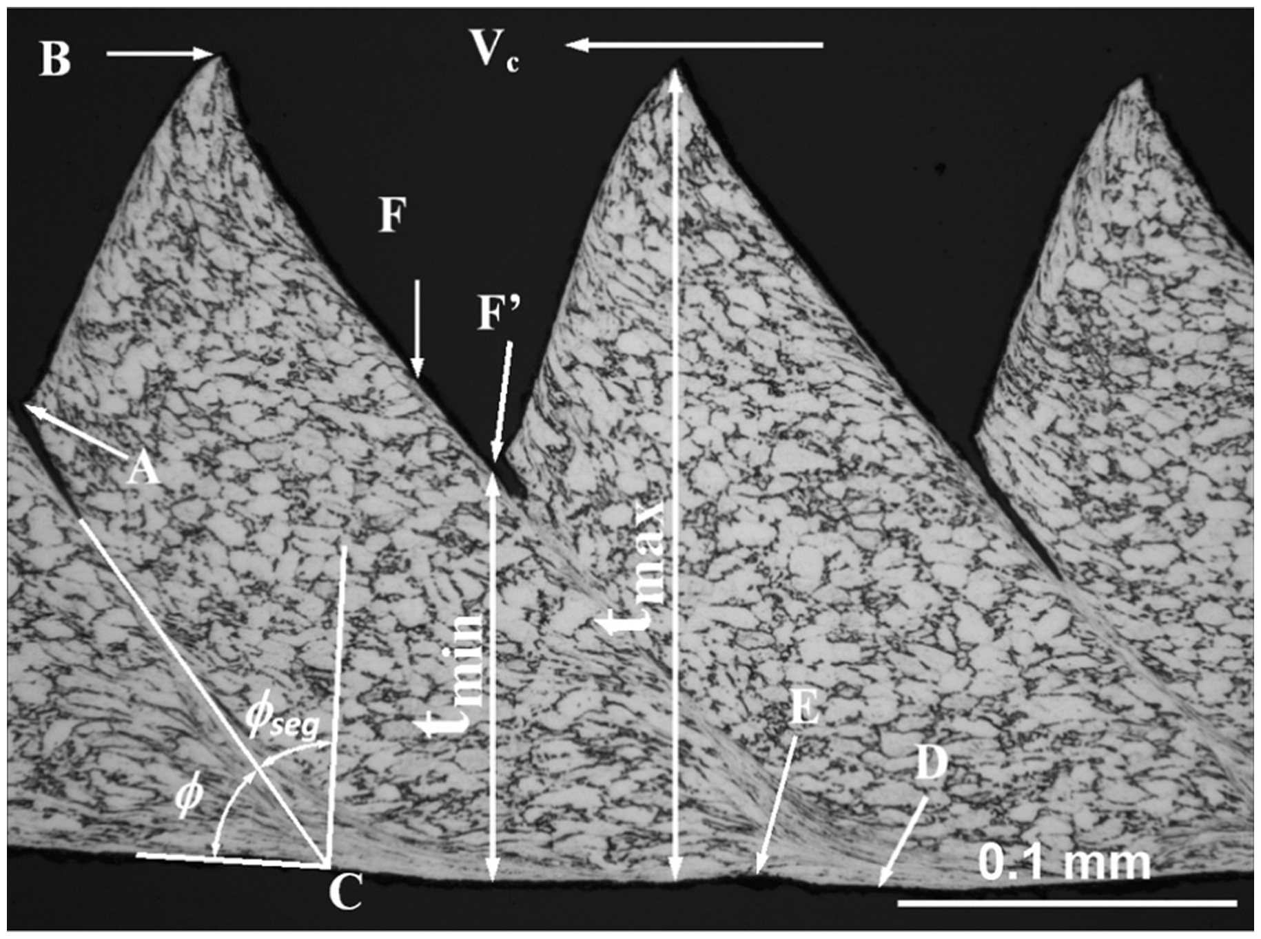
Geometric features of segmented chip made by machining of Ti-6Al-4V alloy at a cutting speed of 150 m/min. 13 Vc is the chip velocity.
Considerable investigations have been made to quantitatively characterize the effect of cutting process parameters on these features of a segmented chip in cutting Ti-6Al-4V alloy.2,3,20 The effect of cutting speed on the chip geometry depends on the range of cutting speeds, segment spacing, degree of segmentation or chip roughness ratio increases with cutting speed and reaches constant values at a critical cutting speed,16,21 which is a function of workpiece material and feed. 14 The morphology of the segmented chip is also affected by the application of external heating (such as laser beam heating in front of the cutting tool22,23) and magnetic field when machining ferromagnetic steel. 24 Segmentation frequency increases with cutting speed, and the segmentation frequency is also affected by the pressure of coolant during machining with high-pressure coolant 25 and cryogenic coolant.26,27
Flank wear, crater wear and plastic deformation are the dominant tool failure modes during machining Ti-6Al-4V alloy due to the wear mechanisms of abrasion, dissolution–diffusion, adhesion, attrition and plastic deformation.28–32 It has been reported that evolution of the flank wear width and crater wear depth with an increase in the volume of material removed results in gradual changes in cutting forces 31 and cutting temperature.33–35 However, no research on the effect of tool wear condition or the volume of material removed on the geometry of the segmented chip has been published to the authors’ knowledge.
It was found that carbide tool fails as the result of the gradual growth of flank wear during dry machining of Ti-6Al-4V alloy at a cutting speed of 150 m/min from the authors’ previous research. 31 The variation in chip geometric features during the tool wear test at this cutting speed has been investigated in this study. The novelty and significance of this study are listed as follows:
Several important geometric variables of the segmented chip have been investigated and correlated with an increase in the volume of material removed and flank wear width.
A row of plastic deformation dimples has been observed on each undeformed surface of the segmented chip.
Carbon-rich areas in the plastic deformation dimples on the machined surface, slipping surface and undeformed surface of the segmented chip have been identified.
A model is proposed to explain the formation of the plastic deformation dimples and changes in chip geometry with an increase in flank wear width.
Materials and experimental procedures
The workpiece material used in this study is a Ti-6Al-4V alloy, and its optical microstructure shows primary
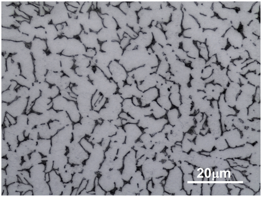
Optical microstructure of Ti-6Al-4V alloy used as workpiece in this study. 31
Turning was conducted on the cylindrical workpiece with starting diameter of 60 mm and length of 150 mm under dry cutting conditions. The carbide insert (CNMX1204A2-SMH13A) supplied by Sandvik was used in this study; its rake angle of the insert was +15° and the entry angle was 45°. With an inclination of −6° in the tool holder, the effective rake angle for this study was +9°.
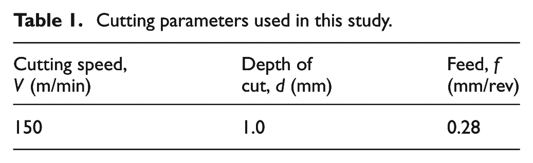
Cutting was performed at a cutting speed of 150 m/min with the constant depth of cut of 1 mm and feed of 0.28 mm as listed in Table 1 and described in the author’s previous work.
31
The cutting speed used is much higher than the cutting speed range (25–40 m/min) that is recommended by the tool manufacturer for industrial production in order to accelerate tool wear while gradual tool wear mode (flank wear) was maintained.
31
The cutting was interrupted and the chip was collected after every 5.2 cm3 of material removed to investigate the effect of the development of tool wear on change in chip geometry. The volume of material removed in each interrupted cut is calculated as
Cutting parameters used in this study.
Due to their helical feature, the collected chips were cut into short segments with a length of about 3 mm and then mounted with epoxy in such a way that they have been erected on their longitudinal edges in order to make the cross section after polishing straight across its length as shown in Figure 1. The geometric variables were measured from the cross section of polished chips, and a total of 50 measurements were performed for each chip geometric variable under each tool wear condition to obtain the average values of the chip geometric variables. The polished chips were etched with Kroll’s reagent to reveal the geometric features and microstructures of the cross section. Scanning electron microscopy (SEM) was employed in order to examine the free surface and machined surface of the chip collected with the different volumes of material being removed. The change in chemical composition on the chip surfaces was identified with X-ray energy-dispersive spectroscopy (EDS).
Results
The cutting tool experiences severe wear during machining; the evolution of flank wear width and tool’s rake angle with an increase in the volume of material removed at cutting speed of 150 m/min is shown in Figure 3. Both maximum flank wear width and average flank wear width increase dramatically when the volume of material removed is greater than 46.8 cm3, whereas the rake angle of the cutting insert reaches its maximum value when the volume of material removed is between 36.4 and 46.8 cm3, followed by a rapid decrease with further increase in the volume of material removed. 31
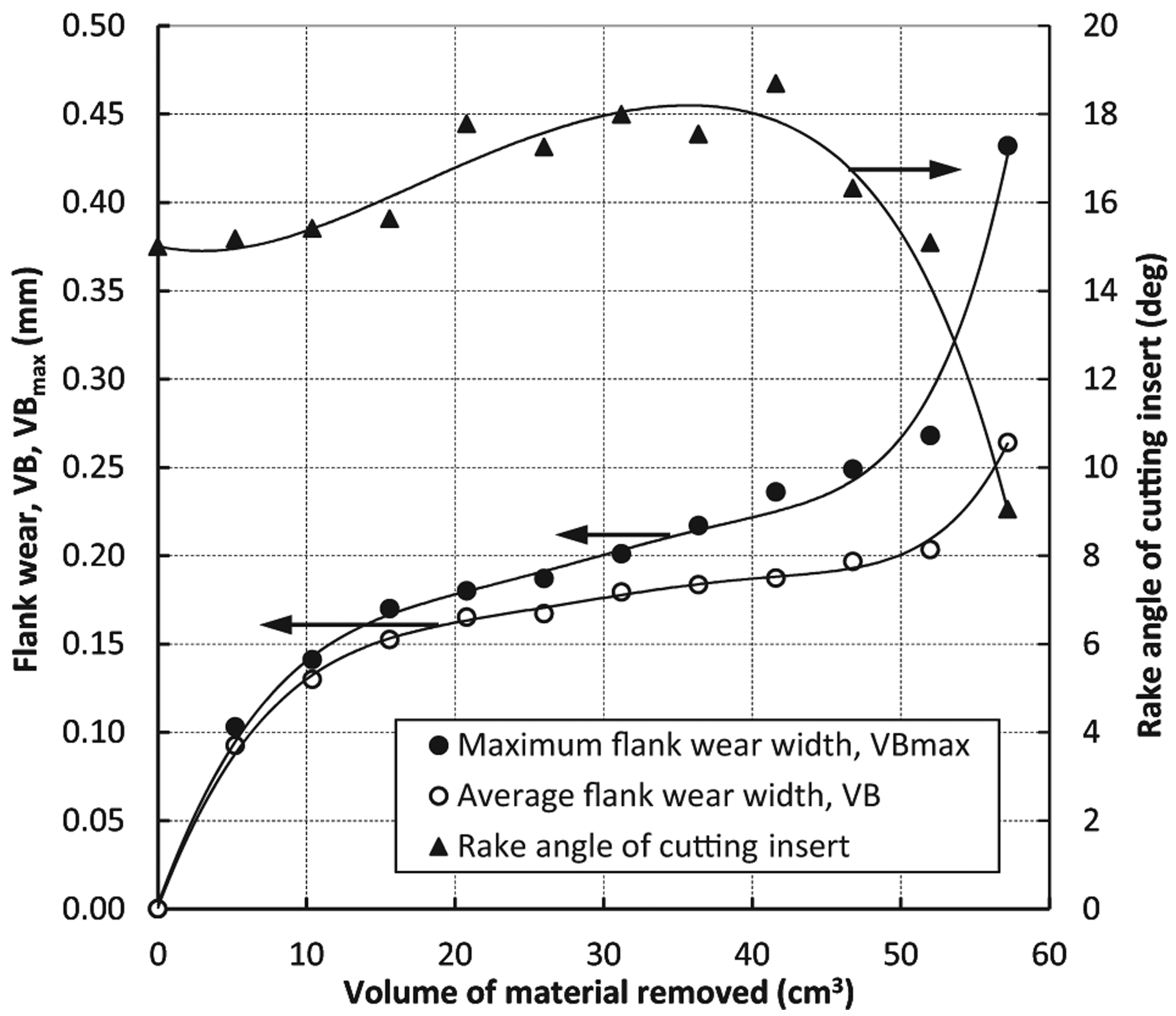
Effect of volume of material removed on the rake angle of cutting insert and flank wear width at a cutting speed of 150 m/min. 31
Variation in the cross-sectional geometry of the segmented chip with tool wear
The cross-sectional geometry of the segmented chip is characterized by slipping angle along with the undeformed surface length, segment spacing and the maximum and minimum chip thickness in this study. Slipping angle (

The length of the undeformed surface is the average length of the cross section of the original undeformed surface


where
The chip thickness is characterized by its maximum thickness (

The cross section of the chips produced with a new cutting tool (the volume of material removed is between 0 and 5.2 cm3) and a worn tool at its end of life (the volume of material removed is between 52.0 and 57.2 cm3) are shown in Figures 4 and 5, respectively. Due to the nature of helical feature of the chip, each photograph was taken for only few saw-teeth whose cross sections were straightly parallel to the polished surface.
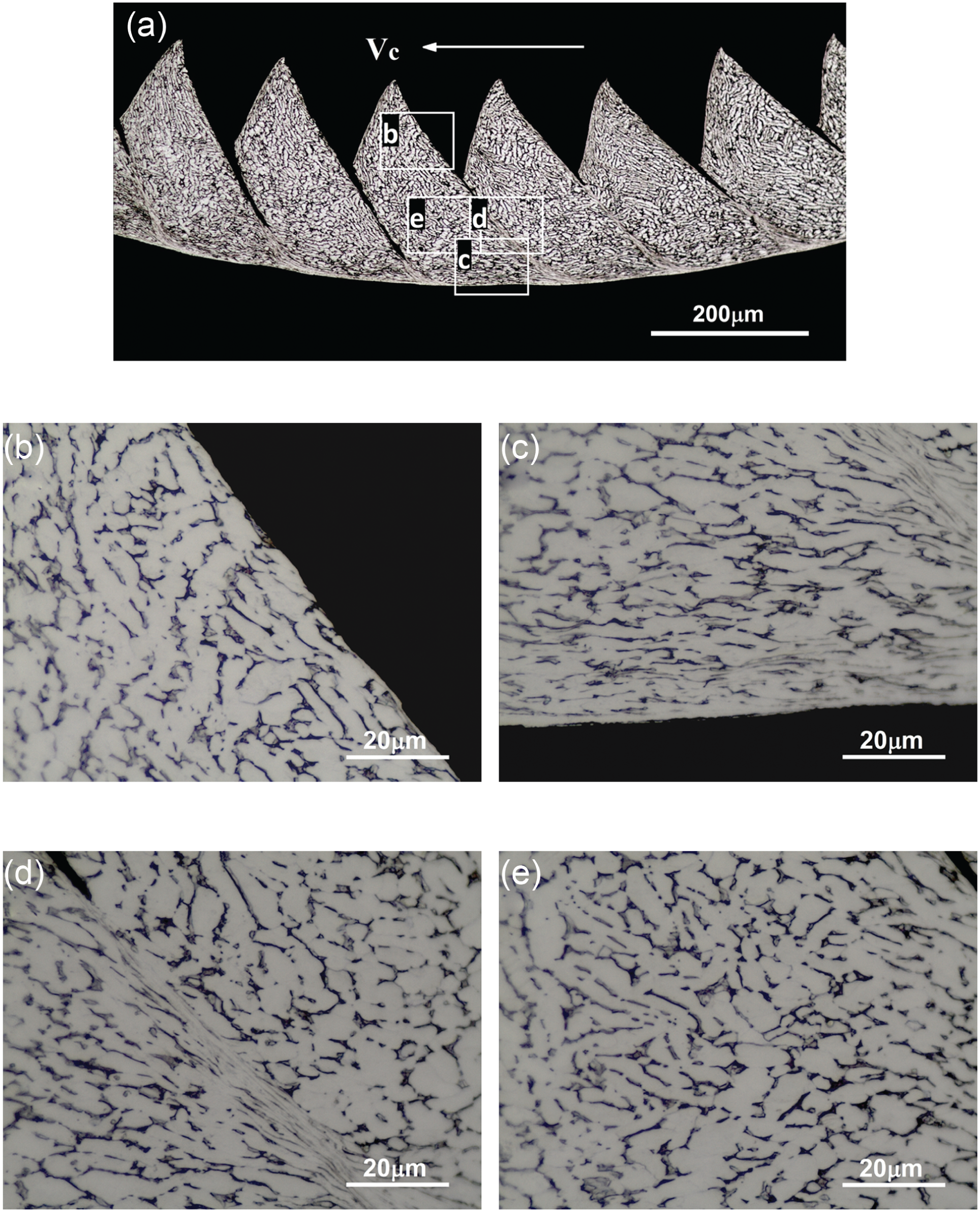
Cross-sectional images of chips made with a new tool at volume of material removed between 0 and 5.2 cm3: (a) for overall, (b) near the slipping surface, (c) near the machined surface, (d) at the shear band and (e) inside the segment. Vc is the chip velocity.
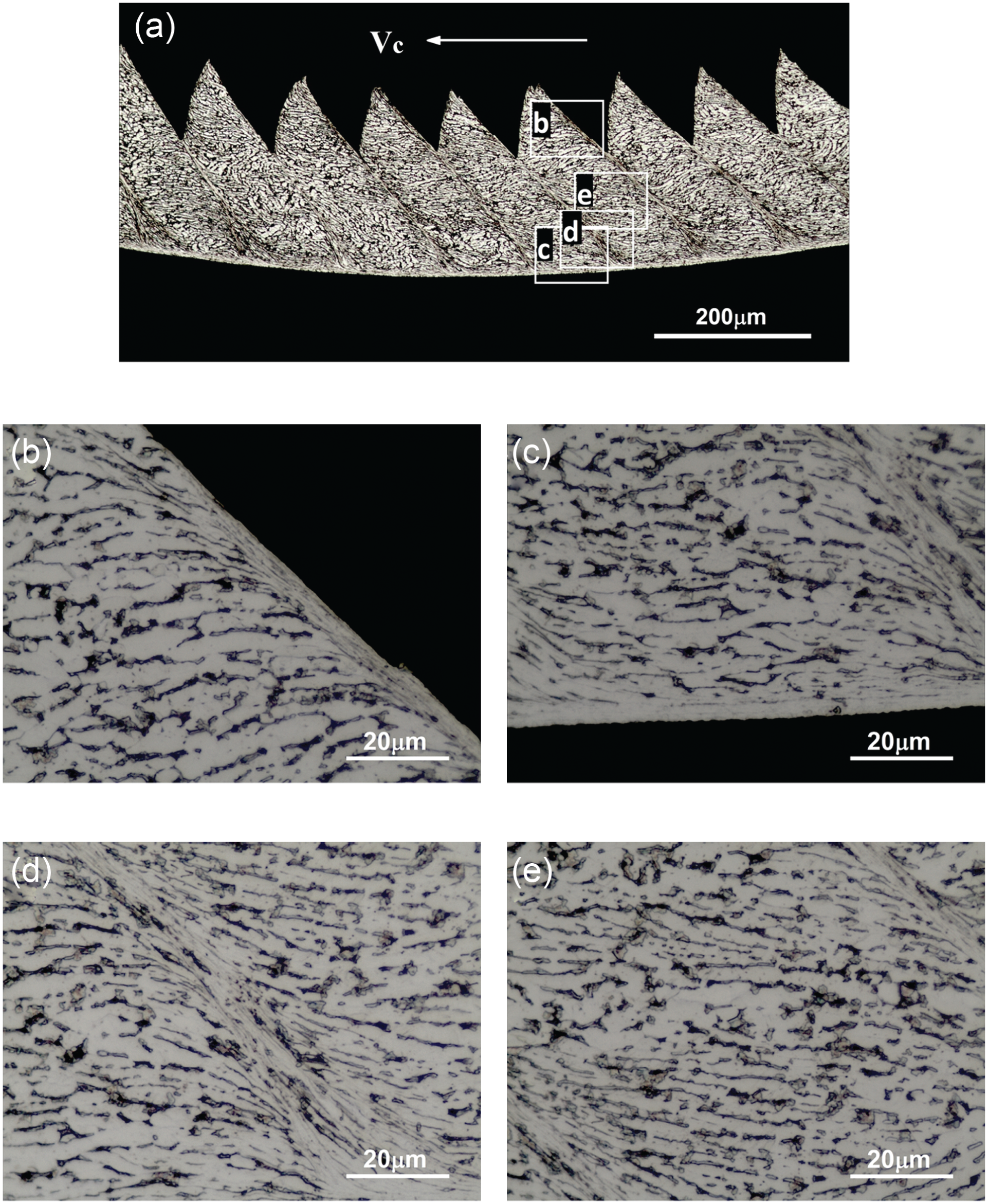
Cross-sectional images of chips made with a worn tool at volume of material removed between 52.0 and 57.2 cm3: (a) for overall, (b) near the slipping surface, (c) near the machined surface, (d) at the shear band and (e) inside the segment. Vc is the chip velocity.
The tendency of crack at the valley point (shown as points A and F′ in Figure 1) between two adjacent segments is reduced in the chips made with a worn tool (Figure 5(a)) as compared with that in the chips made with a new tool (Figure 4(a)). The slipping surface of the chips made with a new tool shows fracture features with grains pull-out (Figure 4(b)) while the slipping surface of the chips made with a worn tool shows a severe shear deformation with clear grain flow underneath the slipping surface (Figure 5(b)). The white layer on the machined surface is continuous and thicker in the chips made by a worn tool (Figure 5(c)) while the white layer on the machined surface in the chips made by a new tool is not continuous and only shows at the intersection with the shear bands (Figure 4(c)). The shear band in the chips made with a new tool is narrower (Figure 4(d)) and the grains inside the segment do not show clear deformation (Figure 4(e)) and are similar to the those in the as-received workpiece (as shown in Figure 2) as described by Xie et al., 6 whereas the shear band in the chips made with a worn tool is much wider with grains flowing in the opposite directions in the two segments adjacent to the shear band (Figure 5(d)); the grains inside the segment show clear deformation flow (Figure 5(e)). These differences indicate that the chip temperature is higher and the friction between the rake face and flowing chip is severer when cutting with a worn tool at the end of its life.
The variation in the average values of chip morphology features with an increase in the volume of material removed is summarized in Figure 6. It is believed that the change in chip formation is the result of progressive change in the tool geometry and an increase in cutting temperature due to tool wear. 34
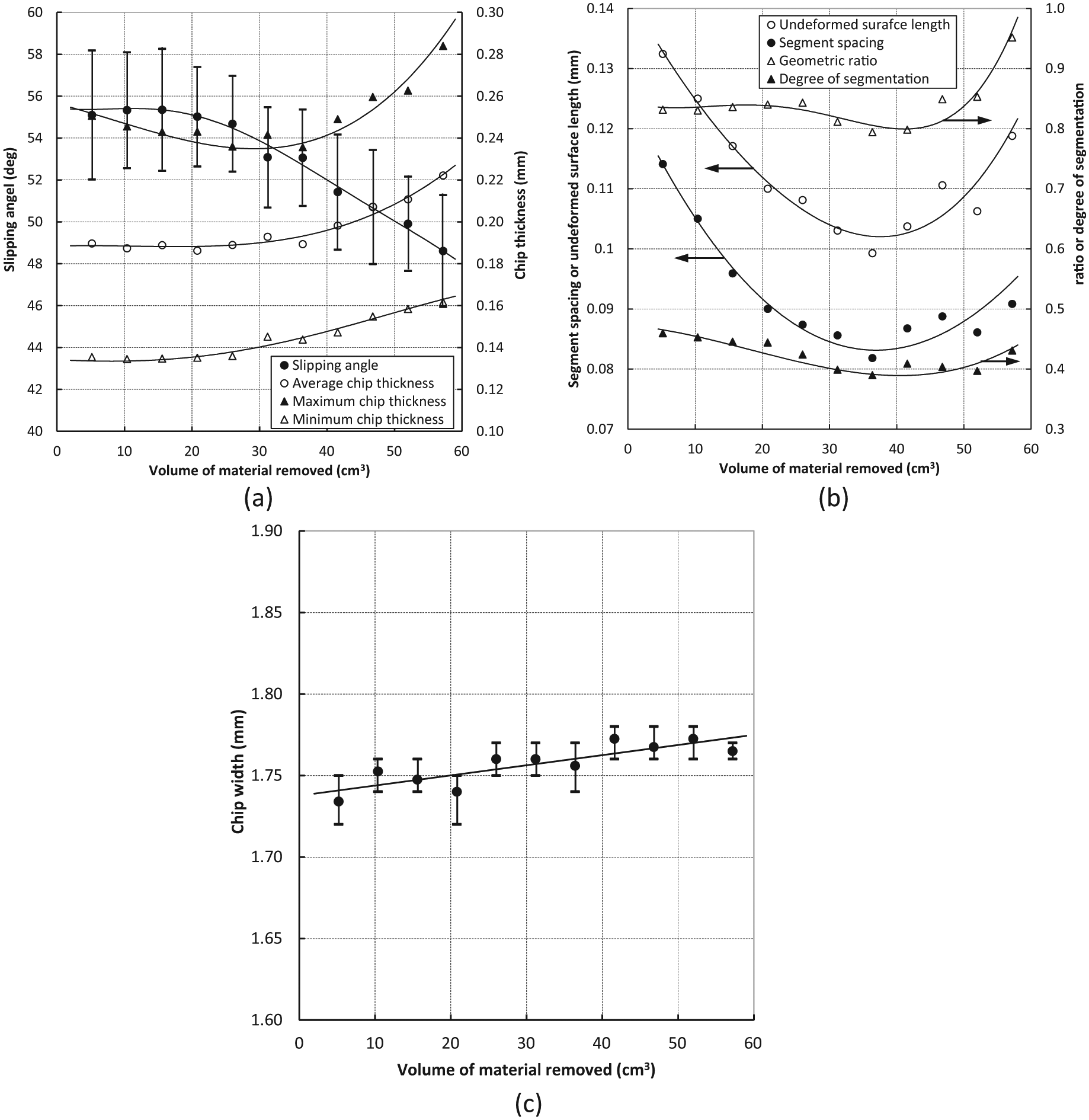
Effect of volume of material removed on the evolution of (a) slipping angle and chip thickness, (b) chip geometric variables and (c) chip width at a cutting speed of 150 m/min.
The slipping angle of the segmented chip was about 55° after removing the total volume of material of 5.2 cm3 (as shown Figure 6(a)), which is the same as the previous result at different cutting speeds. 13 The slipping angle did not change before the volume of material removed reached 26.0 cm3, following which the slipping angle gradually decreased with an increase in the volume of material removed. The slipping angle was 48.6° after removing the total volume of material of 57.2 cm3 (the end of tool life), while the chip segments were still regular since the standard deviation of the slipping angle was maintained about 2.7° after removing the total volume of material of 57.2 cm3.
Chip thickness is also found to vary with the volume of material removed as shown in Figure 6(a); the average chip thickness, the maximum chip thickness (tmax as in Figure 1) and the minimum chip thickness (tmin as in Figure 1) significantly increased with an increase in the volume of material removed from 36.4 cm3; only the maximum thickness slightly reduced with an increase in the volume of material removed up to 36.4 cm3.
The effect of the volume of material removed on other chip geometric features, such as segment spacing, undeformed surface length, degree of segmentation and geometric ratio of the segmented chip, is shown in Figure 6(b). The segment spacing, undeformed surface length, degree of segmentation and geometric ratio were 114 µm, 132 µm, 0.46 and 0.84, respectively, at the total volume of material removed of 5.2 cm3 and started to decrease with an increase in the volume of material removed from the total volume of material removed of 5.2, 5.2, 5.2 and 26.0 cm3, respectively. They all reached the minimum values (82 µm, 100 µm, 0.39 and 0.79, respectively) at the total volume of material removed of 36.4 cm3 following which all the four geometric variables increased with an increase in the volume of material removed. The segment spacing, undeformed surface length, degree of segmentation and geometric ratio were 91 µm, 119 µm, 0.45 and 0.95, respectively, at the volume of material removed between 52.0 and 57.2 cm3 when the tool reached its end of life.
The chip width increased slightly with the volume of material removed (as shown in Figure 6(c)) because the edge of the chip became rough (formation of a burr on the chip edge as shown in Figure 9(c)) and the depth of cut slightly increased due to the thermal expansion of the cutting tool edge at the higher cutting temperature with an increase in the total volume of material removed (evolution of tool wear). This is produced because the cutting edge became blunt as a result of tool wear and the chip built-up edge, 31 which can result in the rough machined surface of workpiece.
SEM observation of the surfaces of the segmented chips
Free surface of the segmented chips
The free surface of typical segmented chips observed by SEM shows lamellar characteristics as shown in Figure 7. This consists of two surfaces for each segment: undeformed surface (A) and slipping surface (B) whose cross section corresponds to lines A-B and B-F′, respectively, in Figure 1. The undeformed surface was produced by the flank face of the cutting tool when the chip was separated from the workpiece in the previous revolution of cut, while the slipping face of the chip was produced during the segmentation in the current revolution of the cut.
SEM images of the undeformed surfaces (A) and slipping surfaces (B) on the free surfaces of segmented chips made at the volume of material removed between (a) 0 and 5.2 cm3 and (b) 52.0 and 57.2 cm3. Vc is the chip velocity.
The undeformed surface and slipping surface of the chips made with the volumes of material removed between 0 and 5.2 cm3 and between 52.0 and 57.2 cm3 at a cutting speed of 150 m/min have been observed using SEM and are shown in Figure 8 at high magnification.
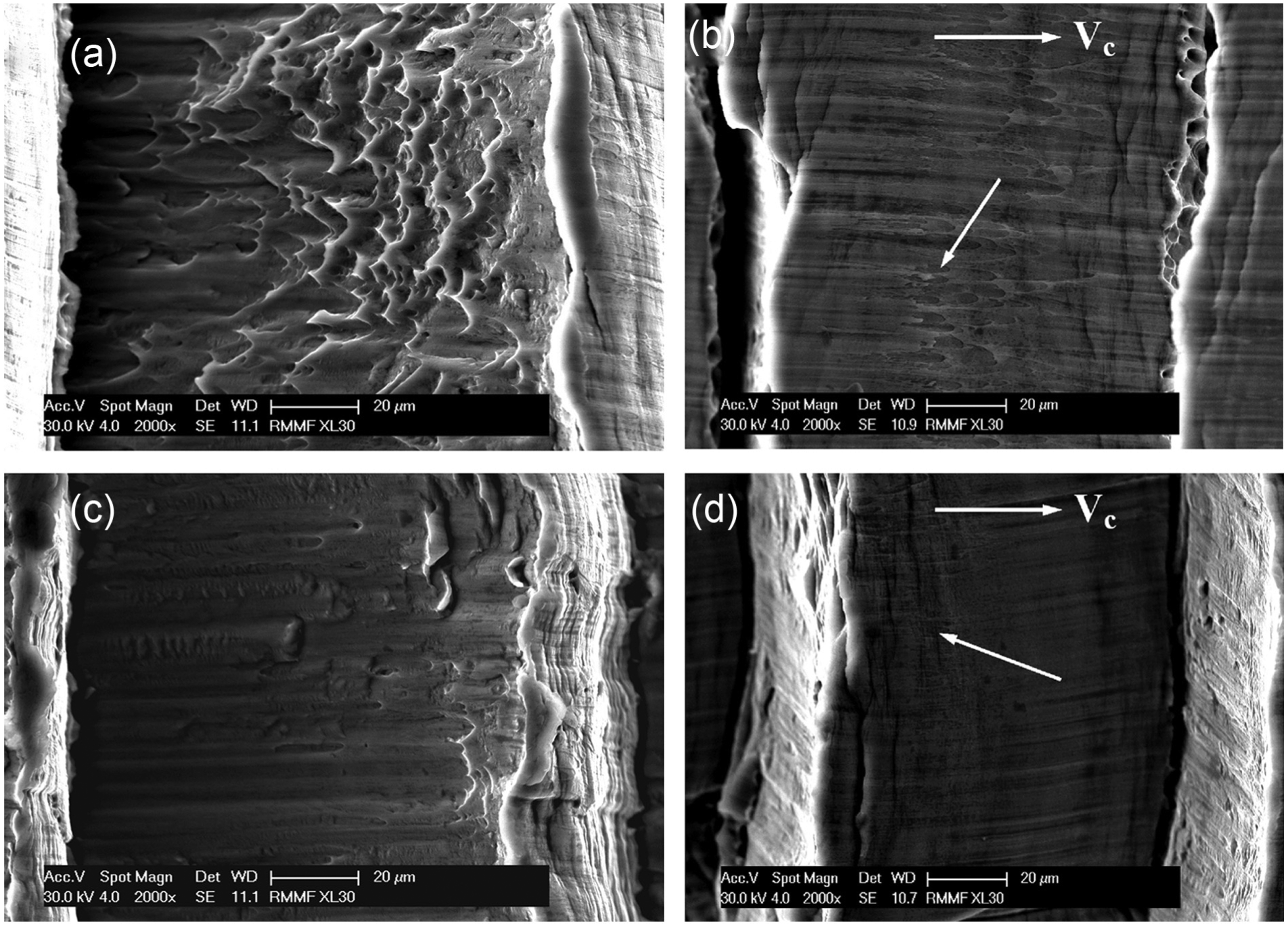
SEM photographs of (a) and (c) slipping surfaces, (b) and (d) undeformed surfaces of segmented chips made at cutting speed of 150 m/min. (a) and (b) are from the volume of material removed between 0 and 5.2 cm3; (c) and (d) are from the volume of material removed between 52.0 and 57.2 cm3. Vc is the chip velocity.
At the volume of material removed between 0 and 5.2 cm3, the upper part of the slipping surface of the chips shows a significant amount of dimples (see Figure 8(a)), which are the result of fracture due to plastic deformation during segmentation, while the undeformed surface of the chips as shown in Figure 8(b) is dominated by the sliding lines which were produced due to friction between the flank face of the tool and newly created chamfer surface of the workpiece in the previous revolution of the cut. Periodic rows of dimples were observed on the undeformed surfaces, one row of dimples on the undeformed surface in each segment as marked by arrows in Figure 8(b) and the surface of the dimple zone is lower than the surrounding sliding zone. This indicates that the chip was removed from workpiece through the growth of voids in the previous revolution of the cut; some of the dimples were not completely removed by the cutting tool because they are deeper than the feed at the location of the dimples. It should be noted that some sliding lines with shallow depth on the undeformed surface did not cross the row of dimples.
At the end of tool life with the volume of material removed between 52.0 and 57.2 cm3 at a cutting speed of 150 m/min, the deformation on the slipping surface shows a clear viscous behaviour (as shown in Figure 8(c)), similar to that observed in laser-assisted machining at low cutting speed, 22 which indicates that the temperature in the cutting zone is significantly higher before segmentation when cutting at the end of tool life compared to that when cutting with a new tool.
The range and size of the dimples on the undeformed surface of the chips that were produced with a worn tool at the volume of material removed between 52.0 and 57.2 cm3 were much smaller (as marked with an arrow in Figure 8(d)) compared to those produced by a new tool. It should be noted that some local damages (grooves as marked with C shown in Figure 7(b)) occurred on the undeformed surface when cutting with worn tool, which were produced on the chamfer surface by the chip built-up edge on the tool’s flank face in the previous cut. The built-up edge is more significant with an increase in the volume of material removed because of the increase in the cutting temperature which is attributed to an increase in friction and change in tool geometry due to tool wear.
Machined surface of the chip
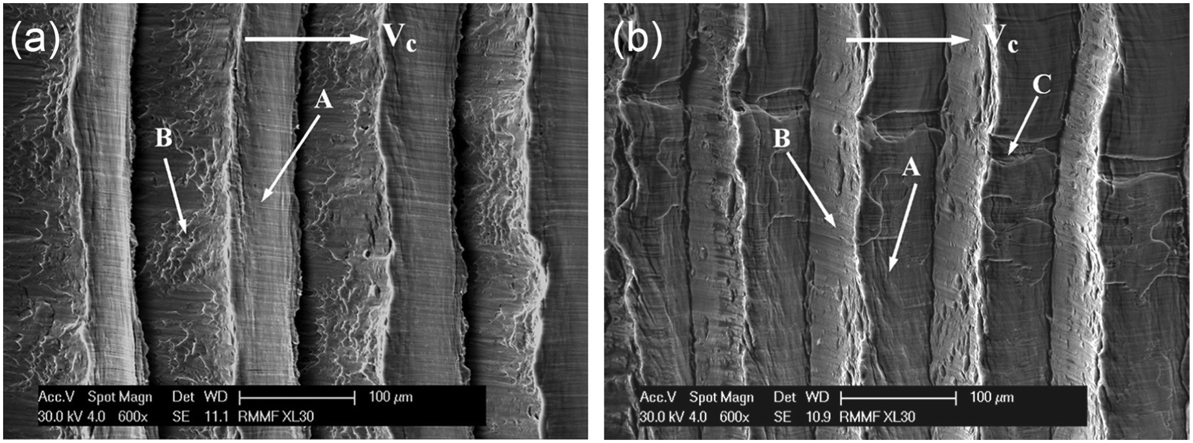
The machined surface of the chip is produced by sliding over the tool’s rake face after the chip is removed from the workpiece. SEM images of the machined surfaces of the chips made at a cutting speed of 150 m/min are shown in Figure 9.
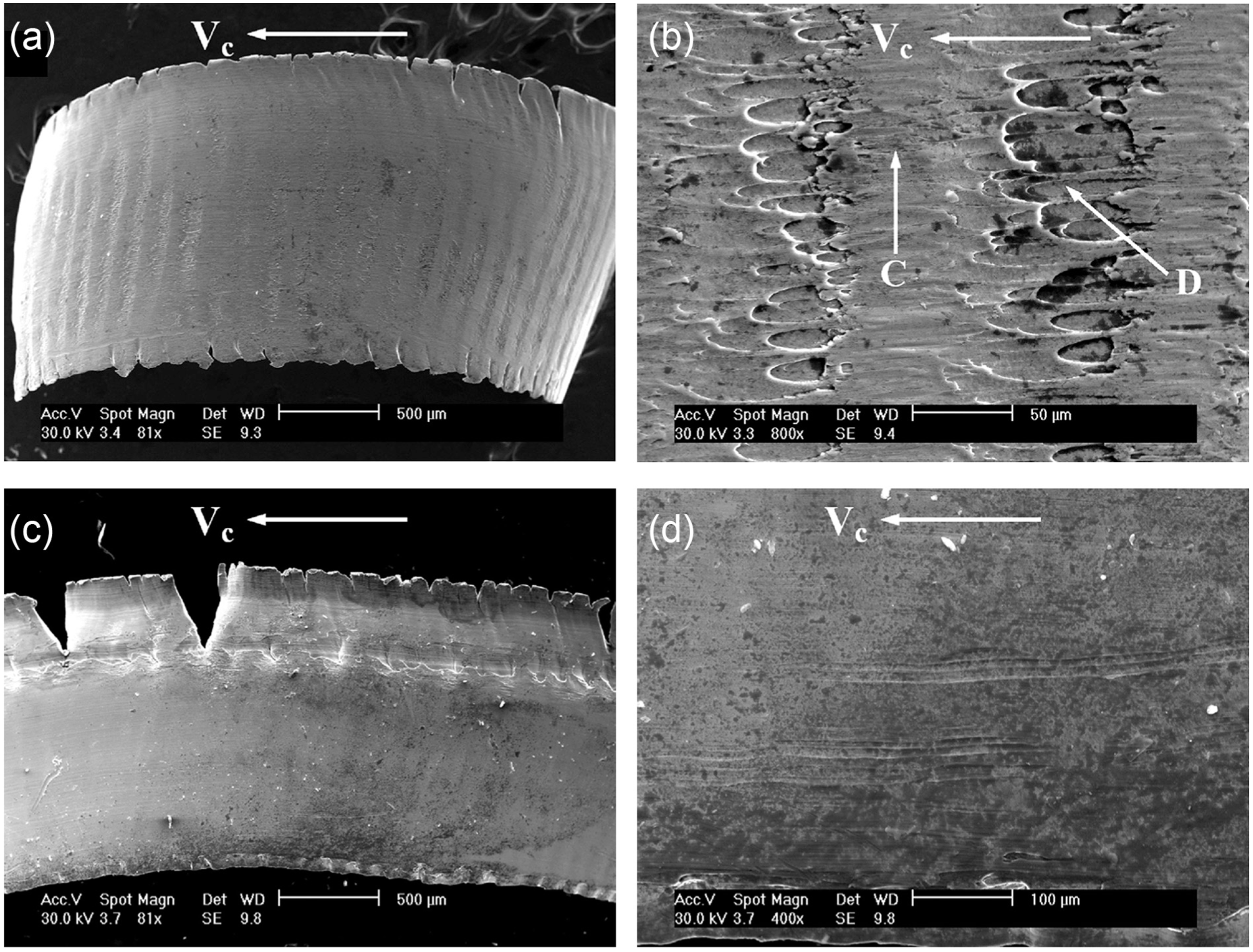
SEM photographs of the machined surfaces of chips made at a cutting speed of 150 m/min. The chips were produced with the volume of material removed (a) and (b) between 0 and 5.2 cm3 and (c) and (d) between 52.0 and 57.2 cm3. Vc is the chip velocity.
The machined surface of the chips made with a volume of material removed between 0 and 5.2 cm3 is characterized as a periodically distributed sliding region (marked with C in Figure 9(b)) and slipping region (marked with D in Figure 9(b)) along the length of the chip. The sliding region shows sliding lines created by the flow of chips over the tool’s rake face, whereas the surface on the slipping zone between two sliding zones shows clearly the plastic deformation dimples.
A significant amount of dark areas was observed inside the dimples in the slipping regions on the machined surfaces of the chips made with the volume of material removed between 0 and 5.2 cm3 (as shown in Figure 9(b)). EDS analysis shows that the dark areas are rich in carbon as shown in Figure 10.
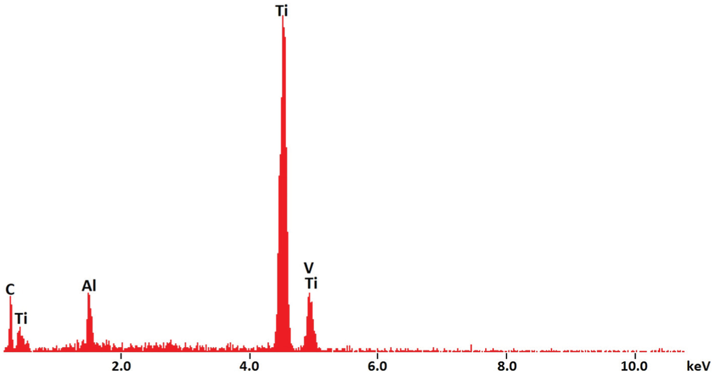
EDS spectrum for dark areas in Figure 9(b).
The machined surface of the chip produced by a worn tool at the end of its life with the volume of material removed between 52.0 and 57.2 cm3 (in Figure 9(c)) does not clearly show the periodic features, and the carbon-rich dark area is distributed across a large region (as shown in Figure 9(d)).
Discussion
Formation of periodic features in the chip
The periodic features of the segmented chip include the lamellar characteristics of the free surface and the periodic appearance of the plastic deformation dimples on both the undeformed surface and the machined surface of the chip in the direction of cutting speed. The latter two features become less significant with an increase in the volume of material removed due to the evolution of tool wear.
The dimples on both the undeformed surface and machined surface of the segmented chip appeared at the locations where the local surface is lower than the surrounding sliding regions as shown in Figures 8(b) and 9(b), respectively; the dimples are deeper and larger in the latter case as they are located at the valley point E of the wavy profile of the machined surface as shown in Figure 1. These dimples on both the undeformed surface and machined surface of the chip are elongated in the tool advancing directions against workpiece and chip compared with the dimples on the slipping surface (Figure 8(a)).
Barry et al. 5 observed the plastic deformation dimples on the machined surface of the segmented chip when machining Ti-6Al-4V alloy and believed that these dimples were formed as a result of periodic fracture of the weld between the chip and tool face due to the stick–slip nature of the chip movement over the tool rake face.
The plastic deformation dimples are formed as the result of growth/breakage of voids during fracture; the flow direction of the plastic deformation dimples on both the machined surface and undeformed surface of the chip is found against the direction of the chip velocity (Vc) over the tool’s rake face (or follow the direction of the cutting tool advancing, V), which indicates that the formation of periodical dimples on both surfaces is associated with the cutting tool travelling direction and chip segmentation.
The sliding lines on the undeformed surface and the machined surface of the segmented chip are produced as a result of the friction between the flank face of the cutting tool and newly formed chamfer surface in the previous revolution of the cut, the friction between the rake face of the tool and machined surface of the chip, respectively. Most of the sliding lines are found not to cross the periodic dimples on both the undeformed surface and machined surface of the chip, which implies that the regions of dimples do not contact the tool faces after they are formed because the surface of dimple regions are below the surrounding sliding regions as shown in Figures 8(b) and 9(b).
Adiabatic shear due to thermoplastic shear instability2,12,36 and periodic initiation and growth of cracks4,37 are the two dominant models in explaining the chip segmentation phenomenon; however, the authors find it difficult to explain the present observations of the segmented chips with the tool wear evolution and chip segmentation with laser beam preheating of the workpiece locally in front of the cutting tool. 22 Sun and colleagues22,38 proposed a model of chip segmentation as illustrated in Figure 11, which includes a cycle of (a) crack initiation and propagation along the cutting direction at point O, (b) fracture of the rigidly displaced chip along the plane B-B′ by shearing and (c) upsetting of the newly formed segment as cutting tool advances.
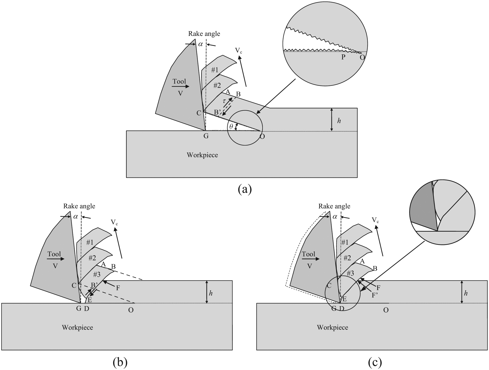
Sequence of chip segmentation for a cutting tool with a positive rake angle: (a) chip displacement along the rake face and crack propagation at point O along the cutting direction, (b) chip fracture and segmentation and (c) upsetting process. 38 Vc is the chip velocity and V is the cutting speed.
Instead of continuous shearing at the primary shear zone, a crack can initiate in front of the cutting edge and propagate along the cutting direction39–41 due to the increase in shear strength and resistance to plastic deformation of the workpiece material at the primary shear zone with high strain rate deformation during cutting. As the machine tool advances to point G as shown in Figure 11(a), the chip is lifted up as it is displaced over the tool rake face during which the tip of crack propagates to point O. Stress is built up in the chip as it is lifted up, and the fracture of the chip occurs when the stress reaches the compressive strength of the chip. A segment with two new surfaces (represented by B-F and D-E) with plastic deformation dimples are produced with the result of chip fracture as shown in Figure 11(b). B-F is the upper part of the slipping surface on the free surface of the chip and is produced as the result of point B shifting to intermediate valley point F, D-E is on the machined surface as the consequence of point B′ transforming to point D after the fracture/collapse of the rigidly displaced chip. Because of the bending D-E plane, it will not contact with the rake face of the cutting tool when the chip moves rapidly over the rake face during the cutting process; therefore, the dimples on the surface D-E remain as those shown in Figure 9(b).
The newly formed surface (repented by line D-E in Figure 11(b)) on the machined surface of the chip increases the length of the machined surface in a segment; hence, the chip geometric ratio (

Because the material is removed from the workpiece by crack propagation at point O, the two new surfaces created by the crack propagation, represented by C-O in the chip and G-O in the workpiece, respectively, are characterized with plastic deformation dimples (as shown in Figure 11(a)). The tip of the crack may propagate deeply into the workpiece with an increase in the open angle of crack (
During the upsetting process when the cutting edge moves from point G to point D, the newly formed segment #3 is pushed up, which moves the segment valley point from F to F′ as shown in Figure 11(c). The surface represented by line F-F′ is the lower part of the slipping surface and does not show plastic deformation dimples because it is produced as the result of the upsetting process.
When the cycle of next segmentation starts, the chip is lifted up by sliding along a line represented by point D against the tool rake face, which results in the formation of significant shear deformation at the intersection of the shear band with the machined surface (point D as shown in Figure 1).
Formation of carbon-rich region
Traces of carbon-rich areas have been observed on the surfaces of the chip. They appear in dark contrast in secondary electron image (SEI) using SEM as confirmed by EDS analysis in Figure 10. The carbon appears rich in the sliding lines on the undeformed surface and the sliding region on the machined surface (as shown in Figures 8(b) and 9(b)) of the chip due to its severe friction with the cutting edge on the flank face and rake face, respectively. The carbon is believed to be lost from tungsten carbide (WC) to form titanium carbide (TiC) on the surfaces of the chips which have been sliding against the tool faces when cutting with a WC/Co tool due to dissolution and diffusion mechanisms,29,30 and the carbon deficiency in WC results in the weakening and embrittlement of the cutting edge. 42
To the authors’ best knowledge, this is the first report that carbon-rich areas were observed in the dimples on the slipping surface, the undeformed surface and machined surface in the segmented chip when dry machining titanium alloys with a WC/Co tools as shown in Figure 12. The carbon-rich particles in the dimples on the slipping surface (Figure 12(a)) and the undeformed surface (Figure 12(b)) of the chips are much finer compared with the carbon-rich area in the dimples on the machined surface of the chips (Figure 12(c)).
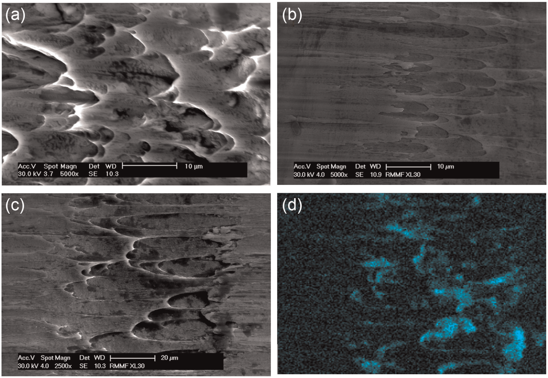
Dimples on (a) slipping surface, (b) undeformed surface and (c) machined surface of segmented chip made at a cutting speed of 150 m/min with volume of material removed between 0 and 5.2 cm3 and (d) the EDS elemental mapping of carbon for the machined surface (c).
Because the dimples on the slipping surface, undeformed surface and machined surface do not physically contact with the cutting tool face during and after they are formed, diffusion of carbon from the cutting tool to these regions cannot explain this phenomenon. The only possible source of carbon for the formation of carbon-rich regions is the carbon-rich particles in the gaseous state.
Emission of fine dust due to high cutting pressure during dry machining has been reported. 43 This dust may consist of carbon-rich (such as TiC) particles when the WC/Co tools are used. Since a significant amount of tool material is lost from the rake face as crater wear, 31 the carbon-rich particles are more likely to be removed from the tool–chip interface on the rake face of the cutting tool.
As shown in Figure 11(c), the chip is lifted up against the tool rake face from point D to point C by sliding on a small contact area around line D, which results in high stresses on the tool rake face. The TiC layer formed on the tool rake face between points C and D is removed in the form of particles due to severe abrasion. This explains why the titanium built-up layer is thinner at the tool–chip contact region adjacent to the cutting edge. 31 The large particles are entrapped in the gap in front of point D between the tool rake face and machined surface of the chip (represented by C-D-E in Figure 11(c)) and deposited there to form large carbon-rich areas in the dimples in the slipping region on the machined surface of the chip (as shown in Figure 12(c)). The small particles form smoke around the cutting zone and can be deposited in the dimple regions on the slipping surface and workpiece surface; the latter will be shown as the undeformed surface of the chip in the next revolution of the cut. The carbon-rich smoke around the cutting zone will be further investigated by spectroscopy in a follow-up publication.
Effect of tool wear on chip formation
Tools are progressively worn with an increase in the volume of material removed or cutting time, which leads to a gradual change in rake angle 31 and an increase in cutting temperature because of an increase in friction between the chip and the cutting tool. 33
The effect of average flank wear width on the geometric variables is shown in Figure 13(a) and (b). Dramatic change in slipping angle and chip thickness occurred when the average flank wear reached 0.185 mm; the strong correlation between the chip thickness and slipping angle with correlation coefficient of
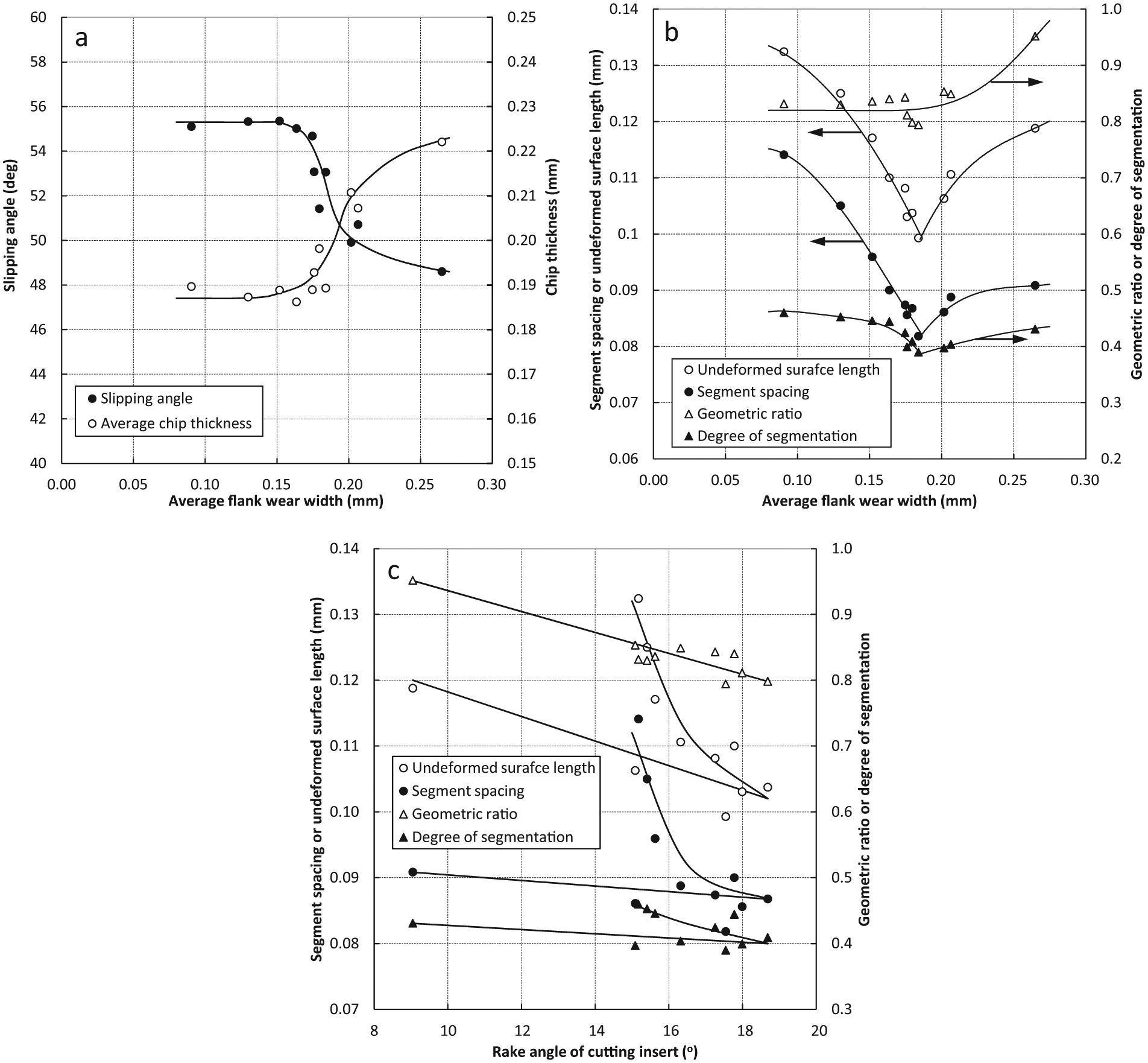
Geometric variables of the segmented chips as a function of the variation in (a) and (b) average flank wear width and (c) rake angle of cutting insert as a result of tool wear.
It is found that all the chip geometric variables generally decrease with an increase in rake angle of the cutting insert as shown in Figure 13(c). However, only geometric ratio of the chip is strongly correlated with the reduction in the rake angle with a correlation coefficient of
The temperature of the workpiece material before it enters the shear zone increases with tool wear because of the increasing friction between the worn tool and the workpiece at both rake face and flank face of the cutting tool. High temperatures enable the material to be deformed more easily at the primary zone; therefore, the level of chip lift-up and open angle at the tip of crack (
Chip formation is believed to almost completely follow the adiabatic shear process when cutting with the volume of material removed between 52.0 and 57.2 cm3 at a cutting speed of 150 m/min. Under this condition, the slipping surface is formed almost due to the upsetting of the material along the shear band at high temperature; hence, no plastic deformation dimple is observed on the slipping surface (as shown in Figure 8(c)); very small periodic dimples are produced on the undeformed surface (see Figure 8(d)) due to a reduction in open angle at the tip of crack (
Conclusion
The geometry of the segmented chip is significantly affected by an increase in the volume of material removed due to the evolution of tool wear. More significant shear deformation occurs inside the segment and on both the slipping surface and machined surface of the chips produced with a worn tool compared with the chips made with a sharp new tool.
With the average flank wear being greater than 0.185 mm, slipping angle dramatically decreases and chip thickness increases with an increase in flank wear. Strong correlation between the slipping angle and the average chip thickness is observed.
At the examined cutting conditions, the three geometric variables of the segmented chip, such as the undeformed surface length, segment spacing and degree of segmentation, show a clear two-stage variation with the evolution of average flank wear; they decrease with an increase in the flank wear width and reach the minimum values at the flank wear width of 0.185 mm following which they increase with an increase in the flank wear width; these changes correspond to the change in rake angle during the evolution of tool wear. However, the chip geometry ratio only increases when the average flank wear width is greater than 0.20 mm.
In addition to the lamellar characteristics on the free surface, the periodic appearance of plastic deformation dimples on both the undeformed surface and the machined surface is observed on the segmented chip made by a new tool and disappears or becomes less significant in the chip made by the worn tool at the end of its life.
The segmented chip is characterized by the plastic deformation dimples on the top of the slipping surface of the chip made by a new tool and smooth shearing on the whole slipping surface of the chip produced by the worn tool at the end of its life.
Traces of carbon-rich areas can be found in the plastic deformation dimples on the undeformed surface, the slipping surface and machined surface in the chip made by a new tool due to the removal of the TiC layer from the tool faces in the form of particles and on the machined surface homogenously over the chip made by the worn tool at the end of its life.
Chip segmentation is believed to be a cycle of (a) crack initiation and propagation along the cutting direction, (b) fracture of the rigidly displaced chip and (c) upsetting of the newly formed segment. The contribution of the first two processes which generate the plastic deformation dimples on the undeformed surface, the slipping surface and the machined surface is reduced and eventually eliminated with the evolution of tool wear due to the increase in the workpiece material temperature before it enters the shear zone.
Footnotes
Acknowledgements
The authors acknowledge the facilities, and the scientific and technical assistance, of the Australian Microscopy & Microanalysis Research Facility at the RMIT Microscopy & Microanalysis Facility, at RMIT University.
Declaration of conflicting interests
The author(s) declared no potential conflicts of interest with respect to the research, authorship and/or publication of this article.
Funding
The author(s) disclosed receipt of the following financial support for the research and/or authorship of this article: This work was supported by the Defence Materials Technology Centre (DMTC) and the Queensland Centre for Advanced Materials Processing and Manufacturing. The DMTC was established and is supported under the Australian Government’s Defence Future Capability Technology Centres Programme.