
Abstract
This work investigates the areal effect, a smoothing of the surface areal topography in measurements from optical instruments that arises from the use of discrete pixels. Two-dimensional and three-dimensional models for the process of acquiring areal topography data were developed and applied to three-dimensional reference surface textures of various traditional machined surfaces that were measured by an atomic force microscope. Sets of reference surface areal data were stitched by a three-dimensional stitching method prior to their use in simulations. Roughness parameters and cumulative power spectra of areal topography of the specimen surfaces measured by coherence scanning interferometry were calculated and compared to the results from the simulated profiles. The results from the simulated data profiles showed good agreement with profiles measured by a coherence scanning interferometry microscope. Finally, the relationship between the pixel size of the optical instruments and the resulting reliability of the high-frequency components of the acquired surface profiles was investigated with spectral analysis. Selection criteria for the magnification of the objective lens are proposed, which allow determination of the appropriate sensor spatial resolution for measurements based on the surface texture characteristics of the specimen.
Keywords
Introduction
Manufacturing and measurement have a very close relation. Especially, for ultra-precision manufacturing, the measurement process on the machined surface is essential. However, ultra-precision measurement needs a lot of time and effort. So, more efficient measurement process with an instruction manual, such as measurement handbook, can provide highly reliable measured results. The results can provide very important information for more precision and efficient machining process.
Surface texture measuring instruments can be classified into contact and non-contact types. 1 The traditionally used contact-type device uses a stylus to trace a specimen’s surface; this type is still the most widely used in most industrial fields. 2 Contact-type measurement has several advantages: (1) it is easy to use, and surfaces can be measured independently in dirty environments whereas non-contact methods can end up measuring surface contaminants in addition to the surface itself; (2) many commercial measuring products are available that have undergone extensive refinement; and (3) vast quantities of measurement data have been collected in industrial fields for the development of products.
However, contact instruments also have three disadvantages: (1) measurement error caused by the shape of the stylus tip,2–4 (2) plastic deformation of the sample surface at the point of contact due to the normal force of the stylus, 5 and (3) speed limits due to the need to maintain a stable contact state. 6 Optical surface measuring instruments have begun to attract attention due to their ability to take quick measurements that do not damage specimens’ surfaces. 2 However, optical instruments also have several drawbacks: (1) a sensor spatial resolution limit caused by diffraction, which is determined by the diameter of the aperture and the wavelength of the light, and resolution criteria used such as the Rayleigh criterion; (2) smoothing effects arising from the sensor spatial resolution or unit pixel size of the image sensor; (3) difficulty in measuring specimens of high aspect ratio; and (4) sensitivity to the optical characteristics of the measured surface. 7
In spite of these difficulties, through recent developments in optics technology, optical methods for surface texture measurement such as phase-shifting interferometry (PSI), coherence scanning interferometry (CSI), and laser scanning confocal microscopy (LSCM) are spreading rapidly.2,7 Hence, many studies have been conducted on optical measurements of surface topography. 8
In another direction, as manufacturing technology develops, freeform optical surfaces and micro-structured surfaces are spreading into various applications. 9 These freeform optical surfaces can overcome conventional optical limits such as diffraction limits, which have led to the development of nanolenses for ultra-high-resolution image acquisition. 10 Research in this direction is expected to improve three-dimensional (3D) optical instruments to the point where measurement resolution will be limited not by instruments’ optical resolutions but rather by smoothing effects arising from image pixel size.
Most optical instruments construct areal topography using optical information acquired from pixel areas on the specimen. Thus, the sensor spatial resolution of small-area measurements is limited by the pixel area. Optical instruments for surface topography that use image sensors, such as charge-coupled device (CCD) or complementary metal oxide semiconductor (CMOS) sensors, are similarly limited by unit pixel size. Though the pixel area on the specimen surface will become progressively smaller as pixel density increases, this areal effect will still limit the sensor spatial resolution. 11
A number of studies have investigated methods to enhance the reliability of the instrumental results; these methods have included analysis of the actual surface texture distortion due to the characteristics of the probe. For contact-type instruments, the geometric mechanism of the profile distortion caused by the contacting stylus has been investigated since the early 1970s. Radhakrishnan 12 calculated and analyzed the smoothing effect of the stylus using a digitized profile. McCool 13 investigated the nonlinear filtering effect due to the stylus radius on the basis of a distortion model. Mendeleyev 14 investigated the numerical relationships between stylus radius and roughness Rq. Church and Takacs 15 analyzed the spectral density of surface profiles. Yoshida and Tsukada 16 and Leach and Haitjema 17 researched wavelength limitations due to stylus tip radius and defined the critical wavelength to classify the usefulness of short-wavelength components. Lee and Cho 18 proposed a method to determine the optimal stylus tip radius considering surface texture characteristics based on the results of spectral analysis. Gallarda and Jain 19 proposed an imaging process model for interactions between an atomic force microscope (AFM) tip and the surface geometry from the viewpoint of morphological operations, although their model was effective only under some limiting assumptions about the probe shape. A method of nonlinear transformation to restore real surfaces using a measured image and a non-ideal tip has been proposed.20,21
For optical instruments, Bennett and Mattsson 22 obtained the power spectral density from measured surface texture data. They proposed criteria including spatial frequency bandwidth limits for comparison of various instruments such as AFMs, stylus instruments, and optical instruments. Other studies have suggested methods to reduce the variance of the power spectral density as estimated from measured surface texture.23,24
Based on this background, the following three objectives were established for this study:
Development and comparison of new two-dimensional (2D) and 3D models for profile measurement with optical probes.
Use of profile data of various machined surfaces obtained by AFM for simulated measurements to evaluate the reliability of profile measurements.
Investigation of the relationships between measuring conditions and the resulting characteristics of the acquired data profiles.
As mentioned above, similar studies on profile distortion in a contact instrument by the authors of this article were conducted.3,18 In this study, a similar research methodology is applied. In order to obtain profile data for the measurement simulations, various types of real machined surfaces were measured by an AFM. These original areal measurements contain higher frequency components that cannot be acquired by a typical optical surface texture measuring instrument. The areal measurement data sets were post-processed and stitched by 3D data stitching, for the evaluation of roughness. The assessment of surface texture was conducted according to sampling length, evaluation length, and sampling interval with International Organization for Standardization (ISO).
An efficient optical measurement condition to calculate the roughness parameters Ra and Rq can be presented based on these research results. Especially, this research results are expected to apply to high-precision machining process of an engine cylinder, a large telescope lens, a mirror, and to nano-machining by AFM. 25
ISO standards of surface texture by non-contact instruments
ISO regulates information and measurement standards for stylus instruments.26–28 However, since optical surface measuring instruments have become widespread, it has been recognized that expanded standards are needed. As a result, ISO technical committee (TC) 213 developed additional content for ISO 25178-6:2010, 29 which regulates measuring and analysis methods for surface textures, and new content has been added to the standards for measuring areal surface roughness using optical instruments such as phase-shifting interferometric microscopes, coherence scanning interferometers, and confocal microscopes. ISO/TS 16610-1:2006 30 also contains information on areal filters, which is applicable to areal topography with a conventional profile filter.
In addition to considering compatibility with the vast experience and accumulated data on the use of stylus instruments, it is very important to analyze results acquired by newer optical measuring instruments with conventional evaluation parameters such as Ra or Rq calculated based on line profile data.
2D and 3D measurement models of optical instruments
The images acquired by an optical lens and an image sensor experience distortion due to various physical effects. A key source of distortion is blurring, and there are three types of blur: motion blur due to the relative movement between the object and the optical system, optical blur due to imperfect focus, and a smoothing effect arising from the sensor spatial resolution limit of the image sensor’s pixel size (Figure 1). For assessing surface textures, blur can be reduced significantly by controlling the measurement environment and measurement processes. Various efforts are being made to investigate these blur phenomena in detail and to improve measurement conditions.31,32
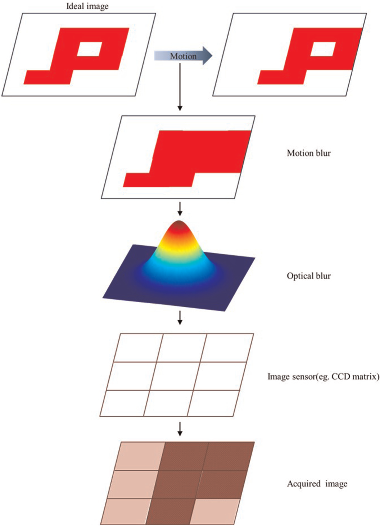
Model of the image formation process used for de-blurring.
Sensor spatial resolution is a very important property in obtaining precise surface texture data. Regardless whether the optical instrument uses a single photodiode or an image pickup device such as a CCD, the resolution of the instrument is limited by optical resolution such as Rayleigh criterion and Airy disk and by the size of the pixels used to describe the specimen surface. In most cases, the pixel size is smaller than the optical resolution, but special lenses are being developed to overcome the present limits of optical resolution. Therefore, the measuring accuracy of instruments will come to depend on pixel smoothing effects or averaging effect.
A typical measurement process model with an optical probe to simulate the distortion process of the surface profile is shown in Figure 2. In this proposed model, it is assumed that the specimen is a Lambertian surface. It was designed only for the analysis of the pixel size effects caused by the relationships between the surface texture properties and the characteristics of the optical path and optical parts in the optical instrument. Other noises caused by light scattering, diffraction, or probe positioning errors are not considered. As shown in Figure 2, the sensor spatial resolution of the optical surface texture measuring instrument is influenced by the areal pixel size on the measured specimen surface.
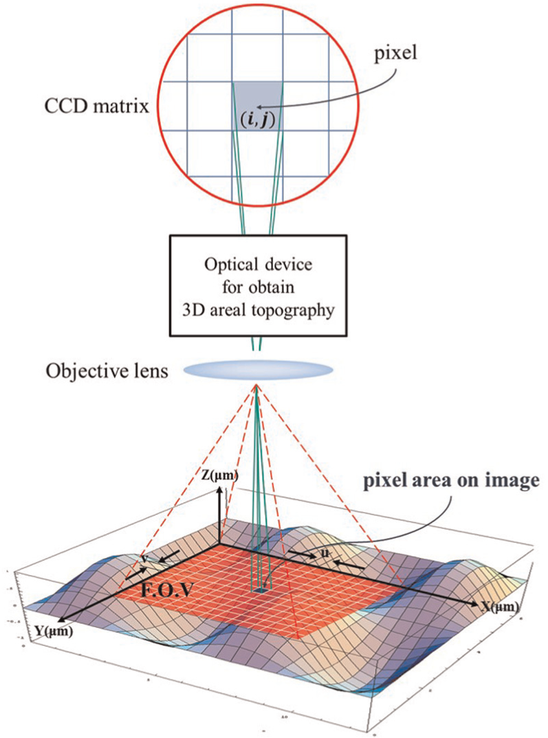
A geometric model of the measuring process.
The effect of smoothing or averaging on the measured profile is summarized in Figure 3. This optical filtration phenomenon arises from the unit pixel shape and size in the optical probe, whose principle is similar to that of the mechanical filtration effect that occurs in contact-based techniques due to the shape and size of the stylus tip when making an enveloped curve of the measured profile.
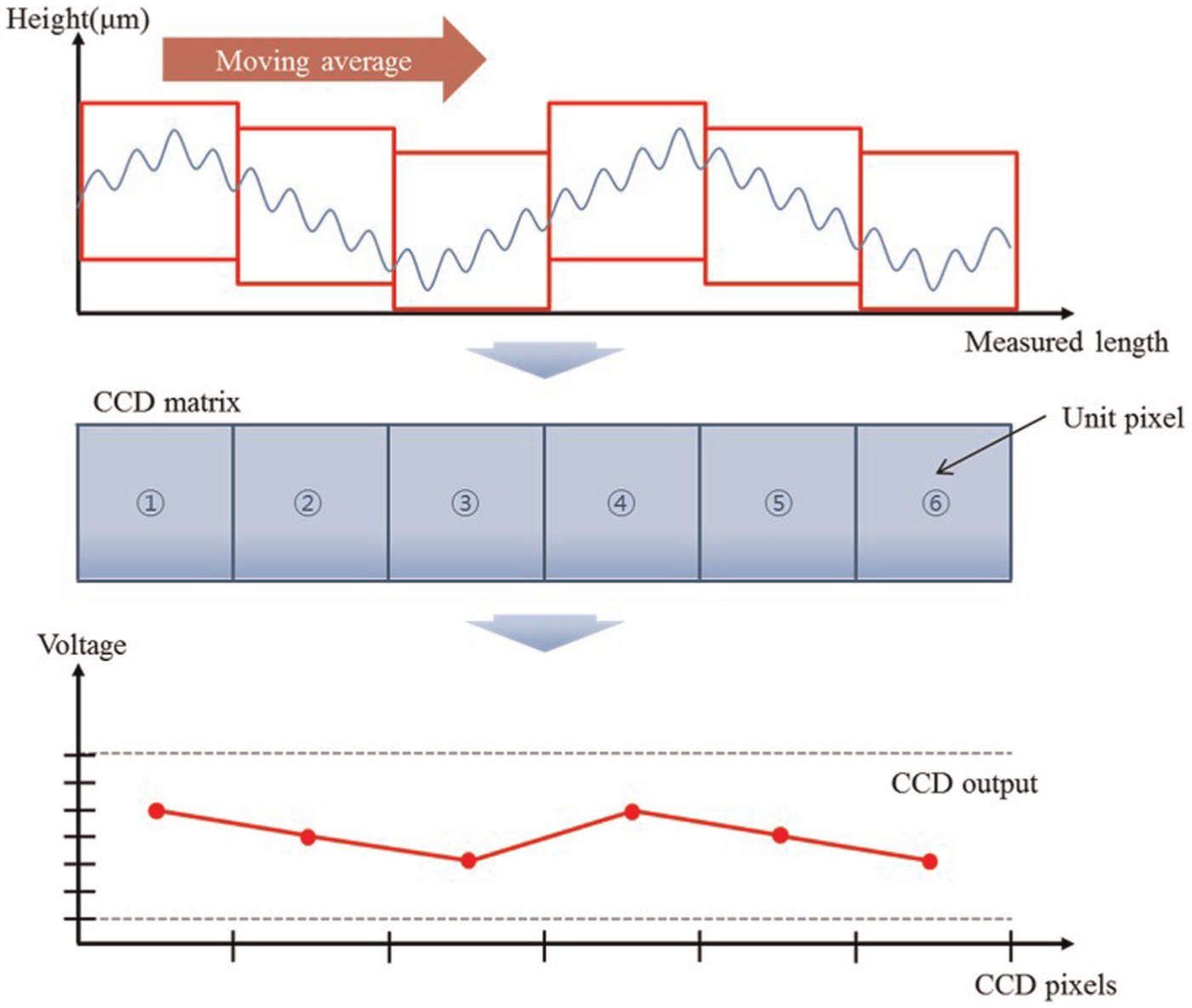
Effects of smoothing or averaging on the measured profile.
In fact, optical measurement using an image sensor cannot acquire micro-topographic information such as small peaks or valleys inside the unit beam spot on the specimen surface. Only an average value for a unit specimen surface area can be acquired by a unit pixel element. Careful 3D analysis is required to accurately investigate this optical filtration phenomenon.
As shown in Figure 4, smoothing effect is applied to the 3D simulation while only resampling process for decreasing the amount of the calculated data is done in the 2D simulation. To analyze the measured profiles obtained by an optical areal measuring instrument, 2D and 3D measuring process simulation models were developed using the following assumptions:
The pixels of the image sensor are ideally fabricated.
Other noises during measurement are sufficiently small that their effects can be ignored.
Only the light beam reflected from the specimen surface can reach the image sensor.
The light incident onto a unit pixel does not interfere with the incident light onto adjacent pixels.
2D and 3D measuring process simulation models.
According to the measuring process model, micro-topographic information can be obtained as a space grid on the specimen surface as shown in Figure 2. The process to generate the output at the corresponding spatial pixel from the micro-topographic information at the 3D surface is modeled as in equation (1). For each cell of the grid, the height value h(i, j) for the unit area (x, y) whose true height is z(x, y) can be obtained as the expectation value Eij [z(x, y)] calculated using the output value of the unit pixel p(i, j) on the CCD. Because the sensor spatial resolutions in the X- and Y-directions are equal for most optical instruments, the equation can be summarized briefly
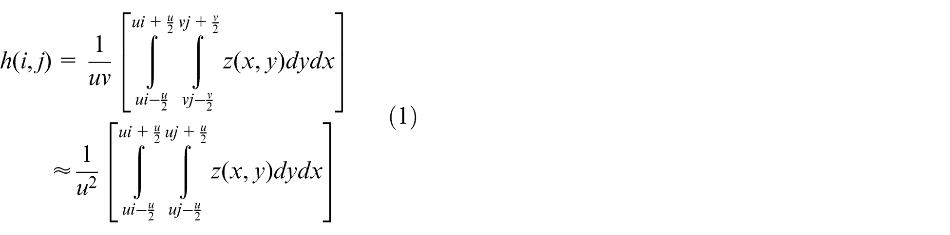
where (i, j) is the pixel at the ith row and jth column in the CCD matrix and u, v is the sensor spatial resolution (μm/pixel).
The mathematical model was applied to 3D surface texture data acquired from various machined surfaces by AFM. These simulated areal measurement results were then compared with the results of the 2D measurement simulation.
Surface profile data for simulation
Various studies have generated surface profiles for simulation in order to analyze the distortion of measured profiles. Thomas et al. 33 and Wu 34 noticed that machined surfaces have fractal characteristics, and they simulated a machined surface using these characteristics. Wu 35 generated a rough surface with Gaussian distortion, and Wu 36 and Manesh et al. 37 generated a surface topography with non-Gaussian distortion characteristics. Nemoto et al. 38 produced a random 3D topographic dataset on the basis of a 2D autoregressive model. However, none of these methods has overcome the limits of expressing 3D shape information from an actual machined surface. Because these methods were established to simulate the significant characteristics of the machined surface, high-frequency components of the generated areal topography may differ from those of the actual surface texture. To ensure the relevance and reliability of the proposed simulation, it is important for the generated areal surface topography to represent the original physical characteristics of the machined surface as precisely as possible.
Considering these limitations, the areal measurement data of the various machined surfaces used in this study were acquired by an AFM (Park Scientific Instruments, AutoProbe M5). The uncertainty level of AFM measurements is ±18 and ±1.6 nm at the 95% confidence level in the horizontal and vertical directions, respectively. 39 These uncertainties are very small compared to the resolution of the optical instrument that this article is targeting; despite this, measurement data by AFM may suffer from significant errors due to the scanner’s nonlinearities and hysteresis. Accordingly, AFM measurements were repeated three times or more, except for the null data. Root mean square values of the difference data between these repeated measurements were calculated to be 0.7 nm or less on average. These AFM areal measurement data provide more detailed surface texture information about higher frequency components for the proposed simulations.
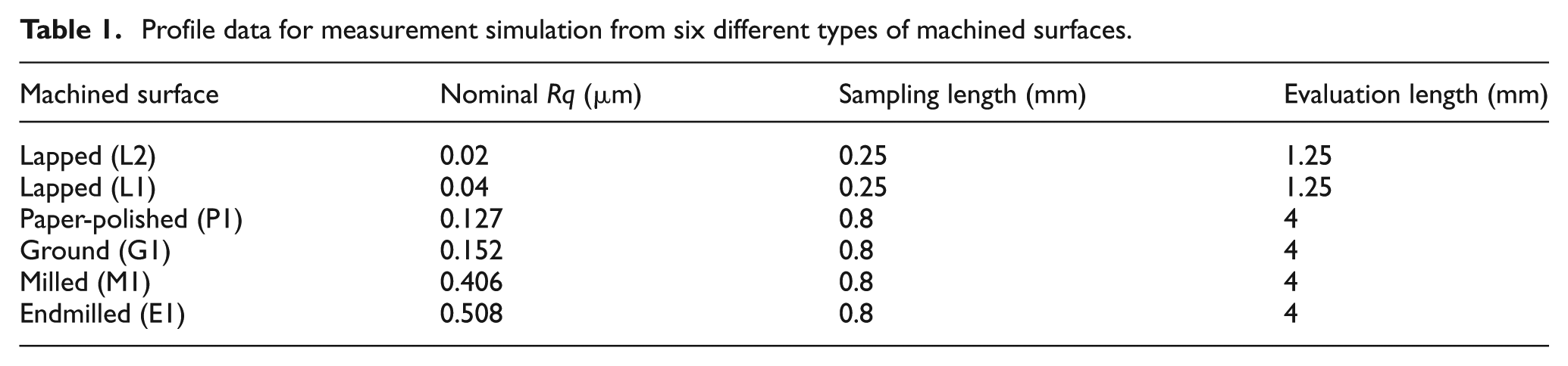
However, these profile data usually are not long enough to be sampled and used for the evaluation of roughness parameters according to ISO 4288:1996. 26 In this study, all the profile data measured by AFM were processed to satisfy the evaluation length by data stitching and merging, as shown in Figure 5, based on the least-squares method and correlation coefficients 40 of overlap areas. Spatial delays were calculated using the maximum value of the 2D normalized cross-correlation function for the data sets in the overlap area. Misalignment of the adjacent areal measurements was corrected using these values of spatial delays, and merged data were computed by applying a weighted average function on the two data areas that coexisted in the overlap area. The stitching error has been confirmed to be about 0.2 nm for the case in which 10 images are stitched by measured data; this stitching error is considered sufficiently small to avoid damaging the reference data. Finally, surface texture data for the simulations with a sensor spatial resolution of about 10 nm were generated using cubic spline interpolation. According to the process described above, six types of measured surface data were obtained from standard specimens (surface roughness standard; Nihon Kinzoku, Japan). The characteristics of surface texture data on six types of machined surfaces used for the simulation are shown in Table 1. The sampling length and the evaluation length are defined as size of the measuring data for the roughness assessment, according to the roughness of each specimen proposed in ISO4288:1996.
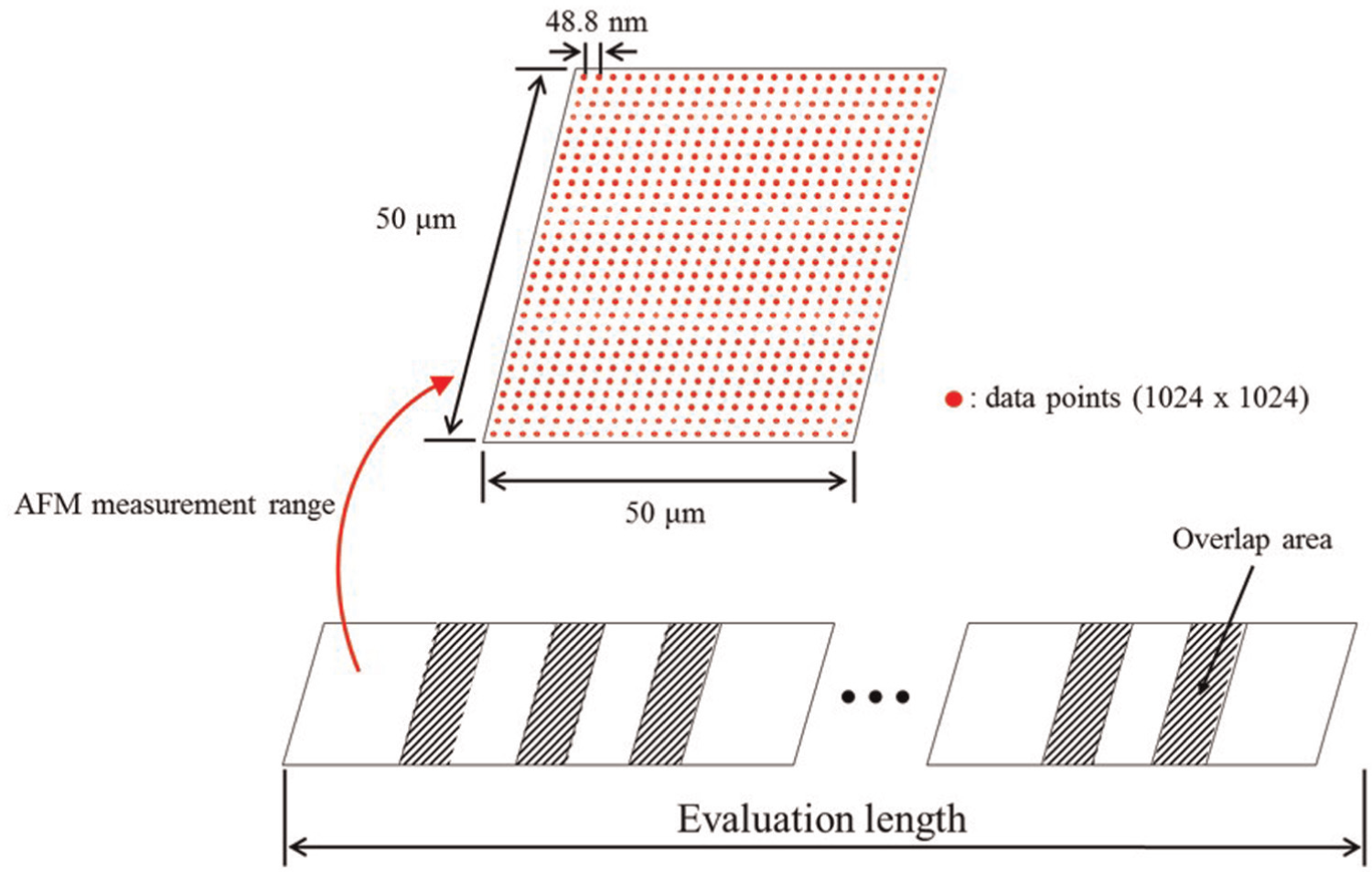
Stitching of the measured profiles by AFM to satisfy the evaluation length for Ra and Rq.
Profile data for measurement simulation from six different types of machined surfaces.
3D measurement simulation
Comparison of 2D and 3D simulation results
The 2D and 3D measurement simulations were performed using the six kinds of stitched areal measurement data obtained by AFM as explained above. Figure 6 shows the simulated 2D and 3D profiles obtained for the original L2 (lapped surface) profiles. The sensor spatial resolution for this measurement simulation is 250 nm. The difference between the 2D and 3D simulation results can be clearly seen in the figure. The 3D measurement model can more accurately simulate the information loss of small peaks and valleys projected onto a unit pixel.
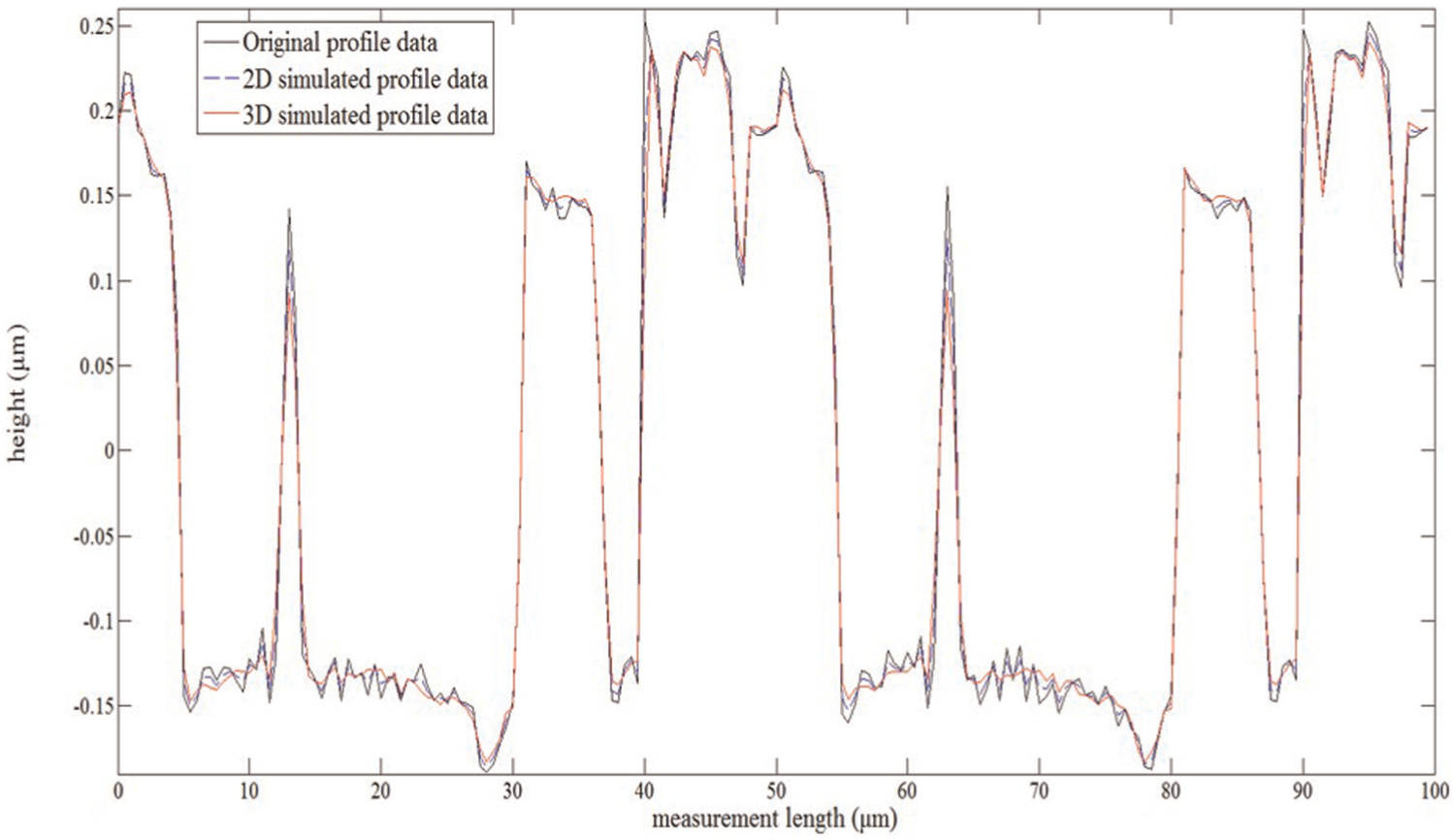
Measurement simulation results for L2 (sensor spatial resolution: 200 nm).
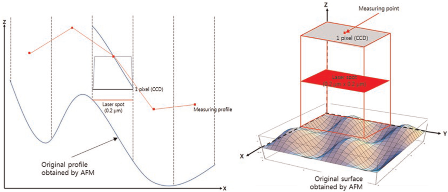
To investigate the different surface measurement outputs that would result from the use of an optical instrument, an anisotropic rough surface measurement was simulated as shown in Figure 7. In the figure, the blue grid represents the 3D surface texture obtained by AFM, while the green grid represents the pixel areas, with green points showing the measured values for the corresponding unit pixels. And the red line is a measured profile to calculate the surface roughness from the output of the optical instrument. Even though the specimen area corresponding to a single pixel is very small, it is confirmed that peaks or valleys exist within this unit beam spot.
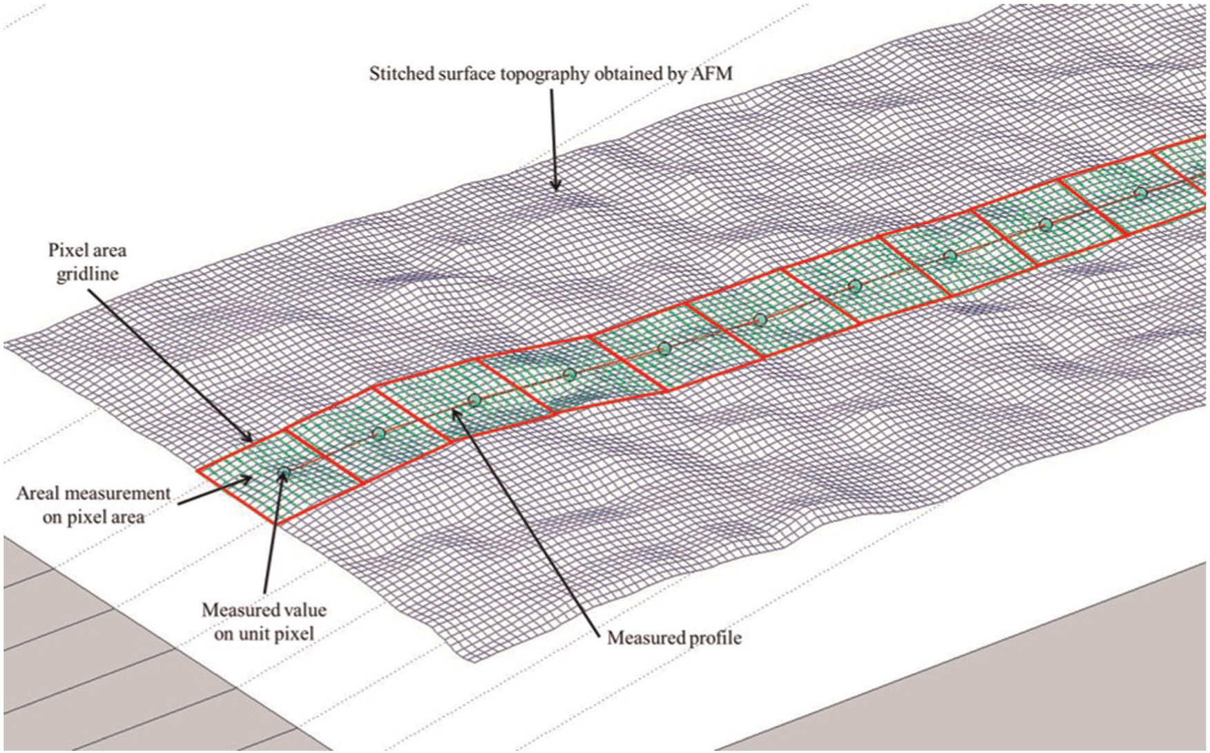
An example of a 3D surface measurement simulation for optical instruments using a CCD image sensor.
Both 2D and 3D optical measurement simulations were performed for the original six machined rough surface profiles. Table 2 shows the values of Ra and Rq evaluated from the simulated profiles according to ISO 4287:2000 for the six different types of profile data and for the various types of standard specimens. The difference between the results from the original surface data and the simulated data demonstrates that optical instruments may have measuring errors as a result of this profile data distortion. The roughness parameter errors of the simulated profiles can be obtained using equation (2) 18
Ra and Rq calculated from simulated measurement profiles (sensor spatial resolution: 200 nm).
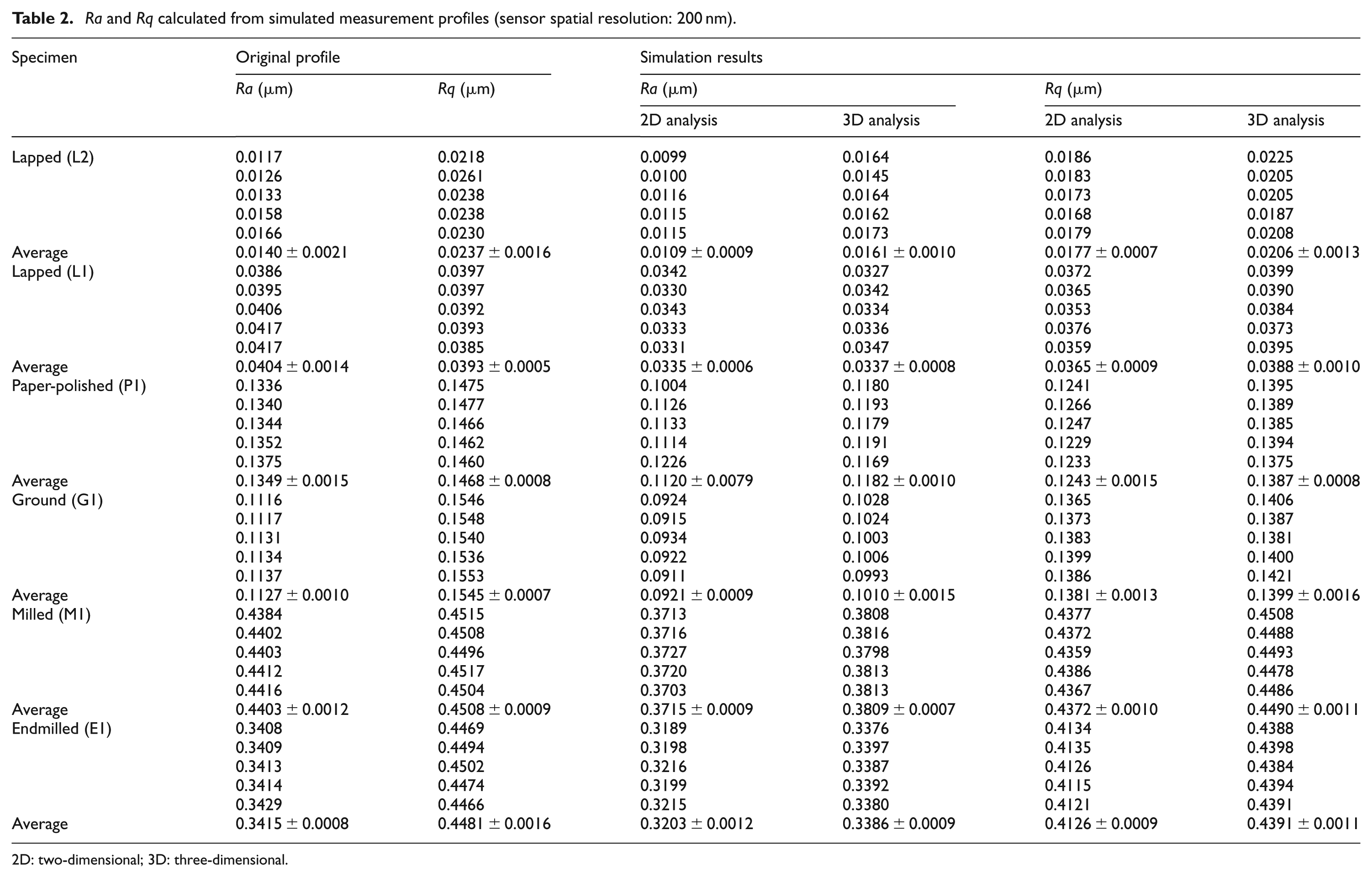
2D: two-dimensional; 3D: three-dimensional.
Figure 8 shows the roughness errors evaluated from the results shown in Table 2. Table 2 is a data to compare 2D analysis and 3D analysis using roughness parameters. Since the two simulation methods were done on the same specimen, the variability of Ra and Rq for the two methods has a good accordance. Therefore, it was checked that different methods bring a shift of average value but maintain the variance. The errors are 22.1% and 25.3% for Ra and Rq, respectively. However, even though the results of both of the 2D and 3D simulation methods reflect distortion effects, the resulting values are different. The maximum error differences in Ra and Rq are 7.1% and 12.2%, respectively. Considering these significant differences, it can be said that the 3D simulation method is more desirable despite its complexity and inconvenience.
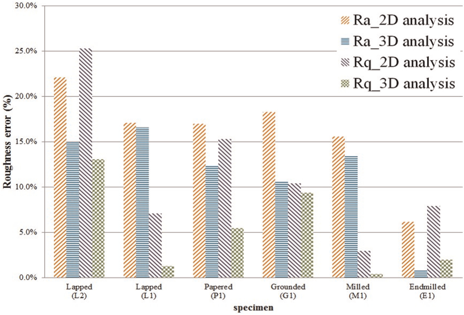
Relative roughness error with a sensor spatial resolution of 200 nm.
Comparison of 3D simulation results and empirically measured profiles
The standard specimens listed in Table 1 were measured again using the coherence scanning interferometer (NV-2000; Nano System, Korea). Measurements were taken using a 50× objective lens and at a sampling interval of 0.20 μm. These empirically measured profiles were also stitched and processed according to the regulations in ISO4288:1996 and then compared with the simulated results to verify the proposed 3D simulation method. Ideally, the actual measurements should be carried out at the same position where the original profile data were acquired by AFM; however, this is not practical. Thus, in this study, the average values of 300 measured results from 30 different points were calculated and compared so that statistically stable results could be obtained.
The measured surface profile data had uncertainty in the reproducibility of the measurements and the evaluations. Considering these uncertainty factors, standard uncertainty was assessed through analysis of variance (ANOVA) for each cause of uncertainty.41,42 The procedure of evaluating the associated uncertainty conformed to the law of propagation of uncertainty as given in the Guide to the Expression of Uncertainty in Measurement. The combined standard uncertainty is given in equation (3)
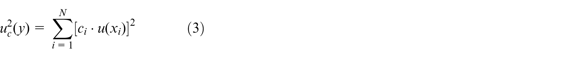
Here,
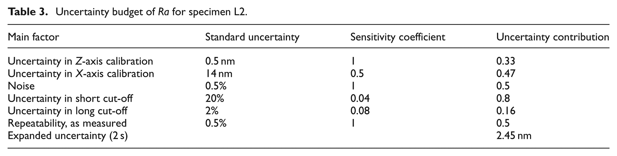
For example, the uncertainty budget of Ra for specimen L2 is shown in Table 3. For this case, the expected deviation is 0.03 nm, which corresponds to 0.02% in terms of Ra.
Uncertainty budget of Ra for specimen L2.
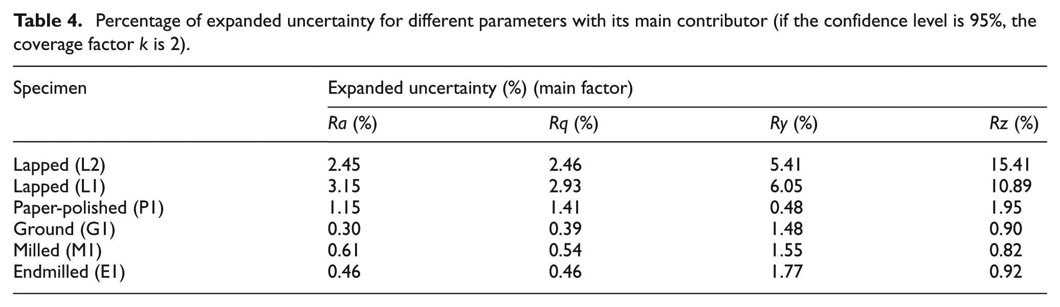
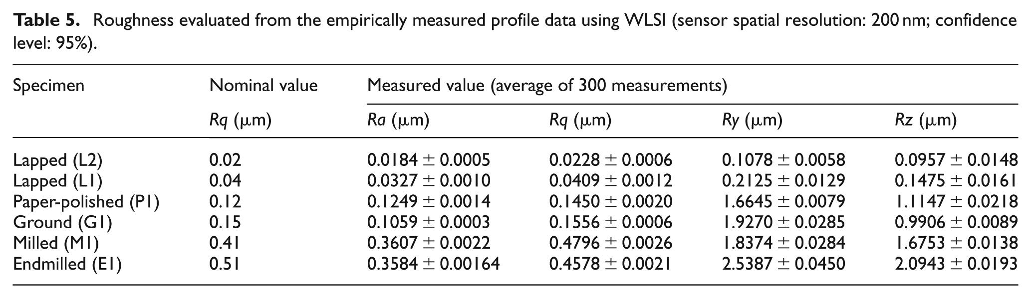
The expanded uncertainties of roughness parameters for each specimen are shown in Table 4, and the roughness parameter results obtained by applying the expanded uncertainties are shown in Table 5.
Percentage of expanded uncertainty for different parameters with its main contributor (if the confidence level is 95%, the coverage factor k is 2).
Roughness evaluated from the empirically measured profile data using WLSI (sensor spatial resolution: 200 nm; confidence level: 95%).
To quantitatively examine how accurately the proposed 3D method simulated the optical rough surface measurement, the results were compared as shown in Figure 9. The difference in the roughness between the results of the 3D simulated profiles and those of the empirically measured data from the white light scanning interferometry (WLSI) were less than 6.4% on average. Thus, it can be concluded that the proposed 3D method can accurately simulate actual optical measurements.
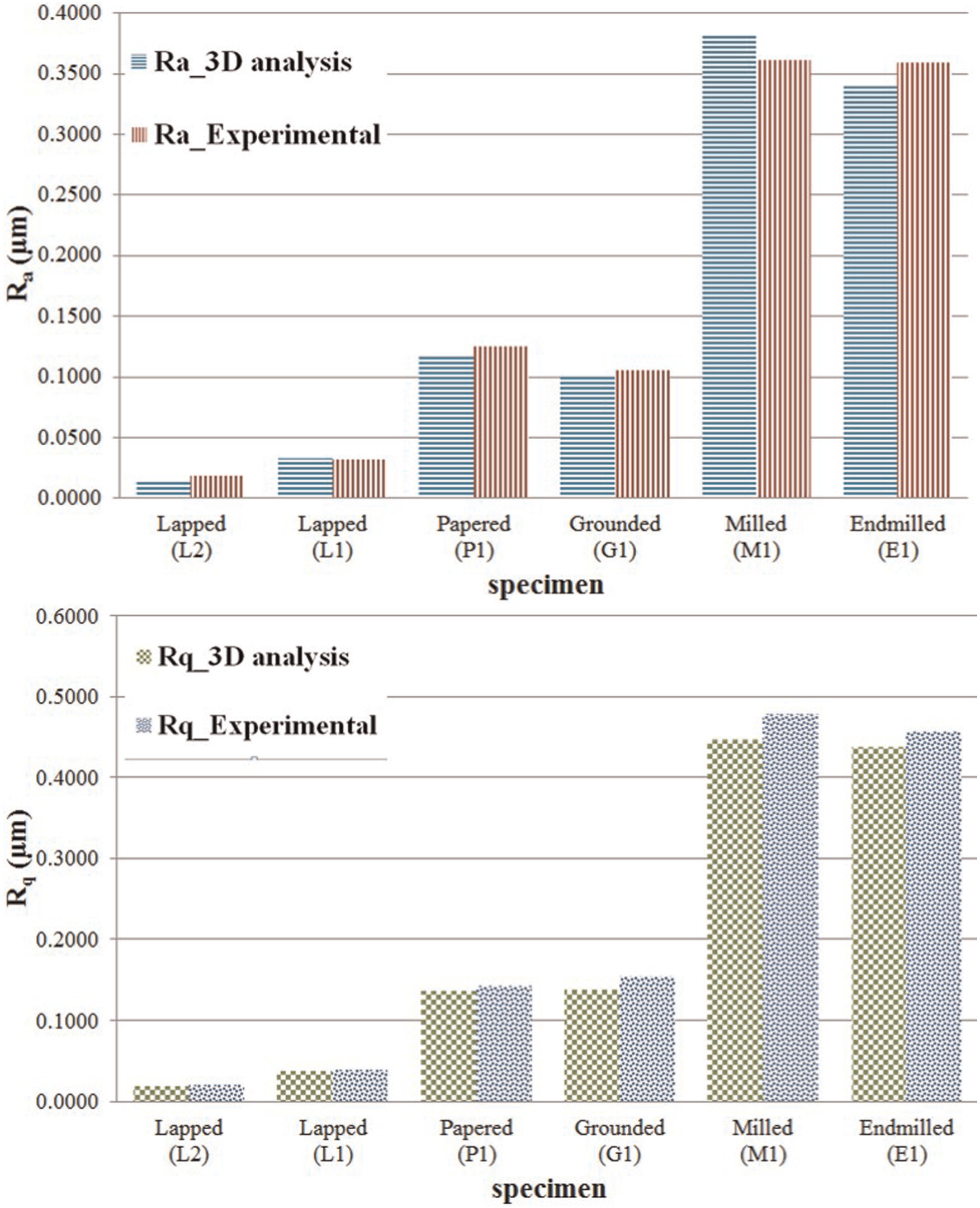
Roughness evaluated from the simulated profile data and the empirically measured profiles (sensor spatial resolution: 200 nm).
Cumulative spectral analysis
When the unit pixel area is larger than the critical wavelength, the shorter wavelength components of the measured surface texture become optically filtered out. This makes the obtained profile smoother and produces unwanted information losses on the shorter wavelength components; thus, the shorter wavelength components included in the measured profile are usually severely damaged and unreliable. To investigate these effects, a spectral analysis method was applied in this study. The critical wavelength is named as short-wavelength limit (SWL) in this article. The critical spatial frequency can then be determined as the reciprocal of the SWL.18,43
The SWL of the measured profile
The normalized cumulative power spectra are computed and examined to determine the frequency compositional distortion of the measurement profile caused by the size of the unit pixel. The power spectra of the simulated profile data are combined and normalized from the base wavelength to the Nyquist wavelength. As mentioned earlier, short-wavelength components are seriously affected by the distortion effect and thus are not reliable. Lin et al. 43 took into consideration the observation that the aliasing effect in measured data is based on areal spectral analysis. They also proposed the concept of the SWL for determining the proper frequency bandwidth. One criterion for measuring bandwidth uses the point where the cumulative spectral power reaches 95% of the total power for measured data. Pawlus and Chetwynd 44 proposed a maximum sampling interval selected by finding the smallest frequency to include 95% of the power for the measured honed cylinder profile. Lee and Cho 18 applied the SWL for a machined profile measured by a stylus-type instrument. They also proposed selection criteria for the stylus tip radius based on surface characteristics. And Giusca and Leach 45 proposed a method to calibrate areal surface measuring instruments using a sinusoidal grid as well as a method for determining the lateral period limit.
Based on this research, wavelength components shorter than the point at which the cumulative power becomes nearly 95% of the total power can be regarded as effective and not severely damaged.3,18,46 In this article, the wavelength at this point is also adopted as the SWL to ensure the reliability of the measured profile. As an example, for the paper-polished specimen (P1), the normalized cumulative power spectra of the simulated 2D and 3D measurement profiles were calculated and are shown in Figure 10 along with their SWLs. The SWL becomes larger as the sensor spatial resolution increases.
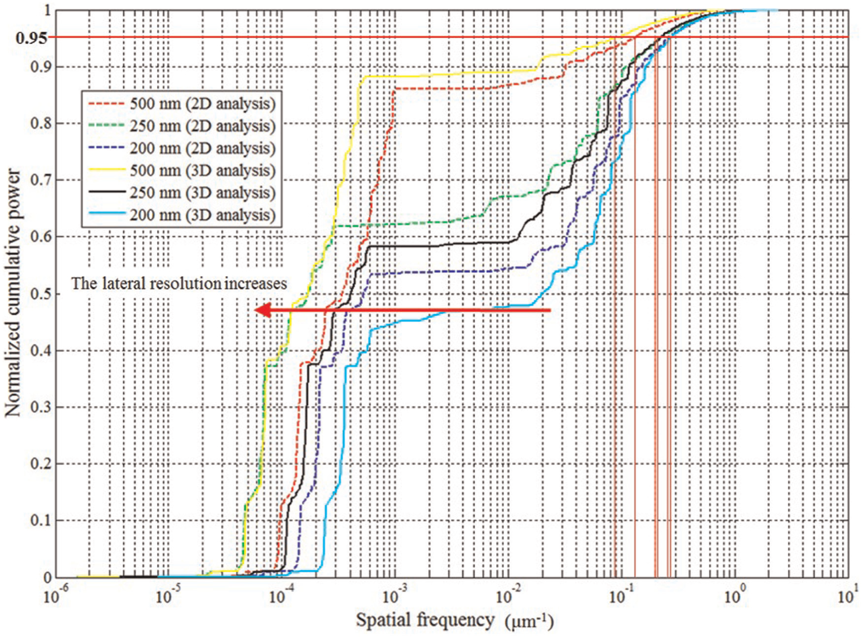
Normalized cumulative power spectra (specimen: paper-polished (P1)).
For all profiles tested above, the amplitude spectra of wavelength components shorter than the SWL declined sharply as the wavelength was decreased. Based on this observation, these shorter wavelength components can be regarded as noise or components with minute amplitudes that can be ignored. This is similar to the results previously published by researchers who studied profile distortion by a stylus tip probe.3,18
The SWL values computed from the 3D simulated profiles of the six types of machined surfaces were plotted according to the sensor spatial resolution as shown in Figure 10. For all types of analyzed profiles, SWLs became longer in proportion to the sensor spatial resolution. Table 6 shows the SWL calculated from all specimens for the sensor spatial resolutions of 0.20, 0.25, 0.50, and 2.00 μm.
SWL calculated from the simulated profiles.
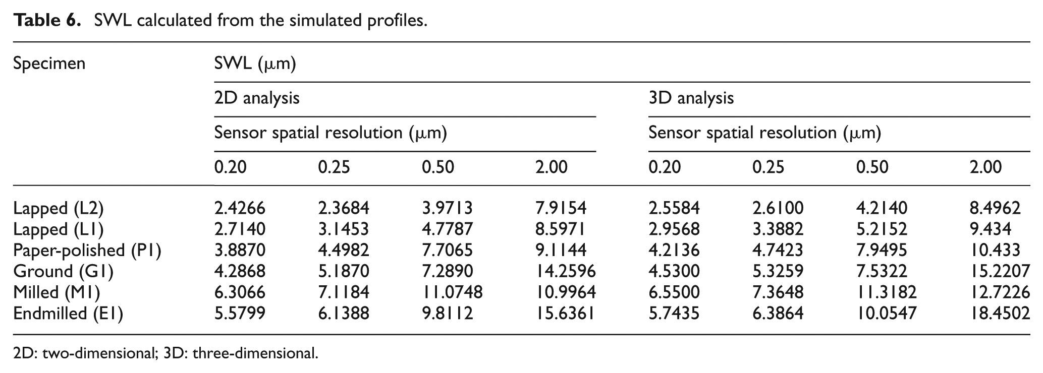
2D: two-dimensional; 3D: three-dimensional.
The relationship between the roughness Rq and the SWL of the available wave components according to the width of pixel area
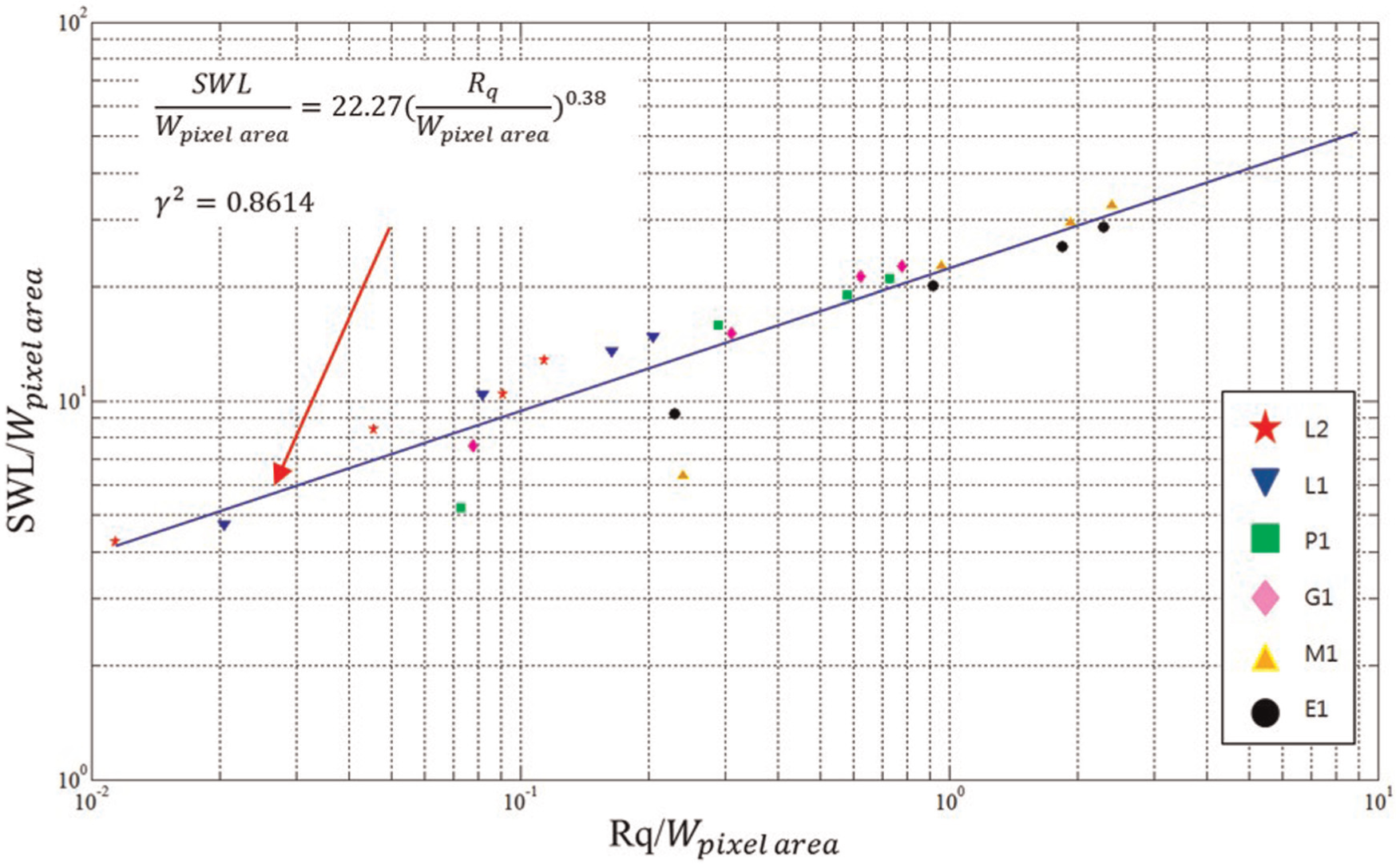
Rq and SWL according to the sensor spatial resolution of the optical instrument.
A numerical fitting by equation (4) was calculated from the analysis of Rq,

As mentioned previously, the empirically measured profile data used for the simulations were obtained from the rough surfaces of standard specimens so that machined surfaces with typical finishes could be investigated. The simulation results can thus be useful for measuring machined surfaces that are lapped, paper-polished, ground, milled, or endmilled and whose nominal Rq values are between 0.02 and 0.51 μm.
Comparison between contact and the non-contact instruments using SWL
Because a vast amount of experimental data have been gathered using traditional contact instruments, it is important to compare the results of optical and stylus instruments. However, such comparisons can be difficult. Herein, the frequency characteristics of the measured profiles are examined using SWL.
The areal measurements from the stylus instrument were first generated by simulation using the same method reported by Lee and Cho. 18 The simulated profiles were generated according to ISO using a stylus of 2 μm tip radius and sampling at 250 nm intervals. SWLs for the profiles from the stylus instrument were computed from these simulated profiles. Optical measurement profiles were also prepared by simulations of 3D optical measurements using the same sampling interval, calculating SWLs from the simulated results. The results are shown in Figure 12. When the sampling intervals were the same, the optical instrument had a 19.5% shorter SWL on average. This means that if there is not a significant amount of scattering or diffraction during the optical measurement, an optical instrument is more accurate than a stylus instrument.
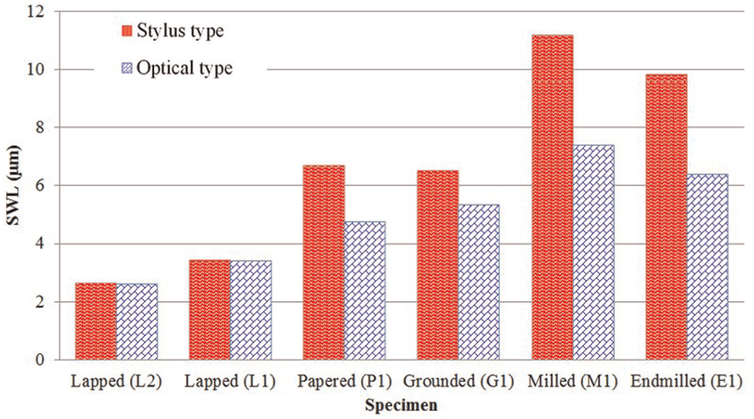
SWLs of the profiles from optical and stylus instruments (optical instrument: 250 nm resolution; stylus instrument: 250 nm sampling interval, 2 μm stylus tip radius).
SWLs were also calculated for the case in which the tip diameter of the stylus instrument was equal to the diameter of the unit reflecting area of the optical instruments (Figure 13). The sampling interval was the same size as the diameter of the stylus tip. The SWLs of the stylus instrument were shorter than those of the optical instrument by about 47%. This assumes that the stylus instrument obtains profile data by contacting points between the spherical stylus tip and the specimen surface during tracing.
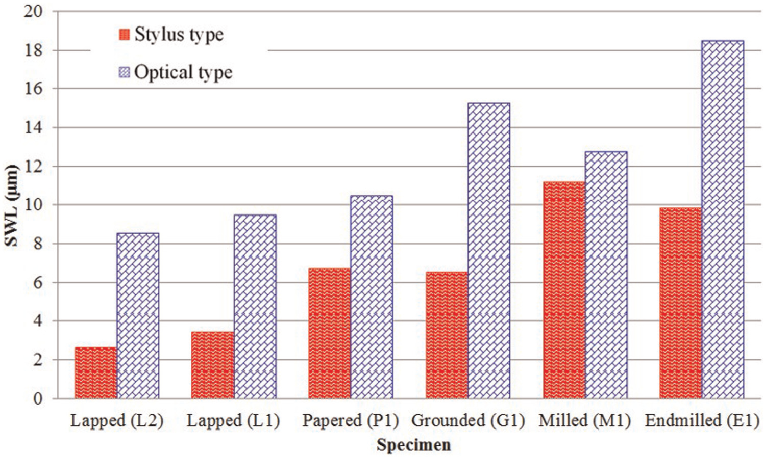
SWLs of the profiles obtained by optical and stylus instruments (optical instrument: 2 μm resolution; stylus instrument: 250 nm sampling interval, 2 μm stylus tip radius).
Because the SWLs for the stylus and optical instruments appear different under different conditions, it is difficult to say which instrument type produces less distortion. However, these results may be used for selecting either instrument type or for setting efficient measuring conditions such as magnification and sampling interval.
SWL and the sensor spatial resolution of optical instruments
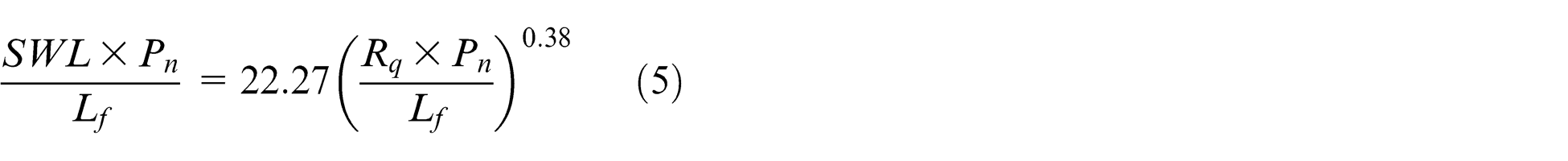
For stylus instruments, the ISO3274:1996 standard suggests simple criteria for selecting the stylus tip size based on the cut-off wavelength. However, in the case of an optical instrument, the sampling interval and the unit light reflecting on an area of the specimen surface are determined according to the magnification of the objective lens. Surface texture is an important property for the tribological and optical characteristics of high-quality machined components, and therefore more effective and reasonable methods are needed for selecting the measurement conditions. The sensor spatial resolution of optical instruments could be selected based on the frequency characteristics of measured profiles using equation (4).
As an example, when measuring a milled rough surface (M1) using a stylus instrument, a recommended stylus tip radius and sampling length can be obtained from ISO4288:1996 and ISO3274:1996 if only the profile height or the irregularity in the surface roughness is considered. However, if using an optical instrument with a sensor spatial resolution of 500 nm for surface measurement, there is no information describing the proper measurement conditions. When measuring high-frequency characteristics of a rough surface, inappropriate objective lens magnification setting may severely distort the high-frequency components of the measured profile. For this case, an SWL of 10.78 μm is calculated from equation (4). This means that if profile data are acquired from a milled surface (M1) according to the ISO recommendations, its higher frequency components at wavelengths shorter than 10.78 μm will not be reliable.
For correct evaluation and precise analysis of rough surfaces including high-frequency components, measurement should be carried out with an objective lens of higher magnification. In this case, if one selects the shortest wavelength of the high-frequency components of the machined rough surface to be analyzed, then one can determine the appropriate sensor spatial resolution of the optical instrument from equation (4) by using the Rq of the specimen surface and the selected shortest wavelength.
Equation (4) was estimated statistically from test specimens, but this method is difficult to apply to all types of machined surfaces. However, this technique provides a simple and easy way to estimate SWL. If needed, more reliable results could be obtained by using additional test results from more appropriate specimens.
The roughness values of the specimen surfaces used for equation (4) and for determining the filter and evaluation length can be estimated by using the values provided by the specimen maker, visual inspection, a control specimen for roughness comparison, and an analysis of the total surface profile orbit graph as recommended in ISO4288:1996.
The unit reflection area size on the measured specimen surface can be calculated using the field of view (FOV) and the resolution of the image sensor. If the image sensor’s pixels are assumed to be square, Pn is the number of the pixel for a column of image sensors, and Lf is the horizontal length of the FOV, then Lf = Wpixel area × Pn ; then, equation (5) can be derived from equation (4) as follows
Because optical instruments usually use one image sensor, the sensor spatial resolution and Pn are fixed for a particular instrument. Hence, the FOV horizontal length Lf can also be determined from equation (5). This equation may be used for selecting an instrument or to set efficient measuring conditions such as FOV or the magnification of the objective lens.
The range and sampling interval of the measured data are very important for calculating the roughness parameters. If a proper measuring condition is not maintained, the calculated roughness parameters cannot be reliable. However, knowing and keeping a proper measuring condition is usually very difficult. In many cases, too much or too little data are acquired and wrong roughness parameter values are obtained. It is expected that this research results can provide the proper measuring condition varying by the precision level of the machined surface.
Conclusion
A new 3D measurement simulation method for optical instruments was developed and its performance was evaluated. This method can be used to determine the effective wavelength component band of a measured surface profile; based on the pixel size of the optical instruments, spectral analysis is used to investigate the reliability of the high-frequency components of the acquired surface profiles. Proposed selection criteria for the magnification of the objective lens allow determination of the appropriate sensor spatial resolution for measurements based on the surface texture characteristics of the specimen.
Footnotes
Declaration of conflicting interests
The authors declare that there is no conflict of interest.
Funding
This work was supported by the Technology Innovation Program (or State-of-the-Art Research Equipment Innovation Program, 10038752) funded by the Ministry of Knowledge Economy of Korea.