
Abstract
Microchannels are primarily used in biomedical devices and microfluidic applications. Fabrication of microchannels has always been a tough task using conventional manufacturing technologies. Various types of materials are in use for fabricating microchannels in different types of applications including metals, polymers and ceramics. A number of methods are in use for fabricating different types of microchannels. These processes include both conventional and nonconventional fabrication techniques such as micromilling, lithography, embossing processes and laser ablation processing. During the recent years, some hybrid techniques have also been developed for fabrication of microchannels. This survey of various literatures reveals a broad spectrum of different processes used for fabricating microchannels. Currently, laser micromachining has been evolved as a potential technology for fabricating microchannels. Laser processing has been proved to be the most time efficient and clean. In this article, fabrication processes for creating microchannels have been reviewed with special emphasis on laser micromachining. This article mostly addresses the fabrication techniques for creating surface microchannels.
Introduction
Fabrication of microchannels is an important aspect in the context of development of microfluidic devices. A number of fabrication techniques have been developed and adopted during the years for different types of applications and materials. These processes include conventional time-consuming technologies such as photolithography, 1 etching 2 and ultrafast femtosecond laser processing. 3 Depending on the applications of microchannel-based devices, different types of materials are preferred. The ever-increasing demand of these microchannel-based devices has also led to the development of several other hybrid techniques to manufacture microchannels in efficient and effective way.
Basically, microchannels are created on polymeric, glass, silicon as well as on metallic substrates. While the most of the polymeric and glass substrates are used in biomedical and chemical devices, the silicon-based substrates and metallic substrates are used for electronics and mechanical engineering–related applications. However, fabricating these microchannels on such substrates in large numbers has always been a difficult task for manufacturers because of the precision required in such products. 4 Lack of suitable technologies for fabricating these devices has hindered the further development of microchannel-based devices. New methods for faster and cheaper production of these devices must be explored for sustainable development in this area. 5
Microchannels and their applications
The shape, size and structures of microchannel vary with different kinds of applications. While most of the microfluidic channels involve high aspect ratio, 6 low aspect ratio channels are also not uncommon in applications such as particle separation devices. 7 In this article, channels having any of the dimensions in micron range (1–999 µm) have been considered as microchannels. The method of fabrication also plays an important role. Microchannels are mostly (except micromilling) fabricated by nonconventional methods.
Microchannels with different cross sections have been fabricated over the years. Most common cross sections include rectangular microchannels, square microchannels, 8 circular microchannels, 9 half circular microchannels, 8 U-shape microchannels and Gaussian beam shape microchannels. 4 Except circular cross-sectional microchannels, all other types of microchannels are fabricated at the surface of the base material. Circular microchannels are generally fabricated inside the material through bulk of it. A thickness of few microns is generally leftover above the circular cross-sectional microchannels along the length for optical and viewing transparency. 9
Microchannel applications can be divided broadly into three main categories: (1) biological applications, (2) chemical applications and (3) electronics and mechanical engineering–related applications. Introduction of miniaturized gas chromatographs and inkjet printer nozzles has led the introduction of microfluidics and these can be considered as one of the foremost developed microchannel-based devices. 10 Later many applications have evolved over the years. For most of the microfluidic applications, the material properties that are important are molecular adsorption, optical properties, machinability, surface charge, electroosmotic flow mobility, electrical and thermal conductivity and many others. 8 Electroosmotic flow is the most common method to introduce flow in microfluidic systems. The study of electroosmotic flow on polymers etched by different processes 11 indicates that both the fabrication method and the material itself affect the electroosmotic flow. Some of the most geometrically simple microchannels can be utilized in making fuel cells which comprise single or double T-junctions. 12
DNA analysis utilizes little more complex networks of microchannel, very similar to networks involved in biosensors. The typical dimensions involved in most of such devices are of the order of 100 µm. 8 Micro total analysis system (µ-TAS) is a platform which has changed the room size laboratory to a laboratory built on a chip. The first TAS device application was a capillary electrophoresis (CE) device and has been widely discussed. 13 Microchannel heat sink is used for cooling the microelectronic chips. These heat sinks are much more efficient and effective than their counterpart devices which are based on forced air flow. Microchannel heat sink consists of large number of microchannels having dimensions of 200 µm × 400 µm × 10 mm. 14 These microchannel heat sinks with different inlet and outlet arrangements of the shapes of U, D, N, V, I and S have been evaluated and concluded that heat sink with inlet and outlet arrangements in V shapes offer the best results. These shapes refer to passage in which cooling fluid flows.
The concept of cooling of electronic chips was first introduced by Tuckerman and Pease. 15 It has been observed that both the geometry of microchannels and substrate materials affect the performance of microchannel heat sinks. 16 The efficiency of solar photovoltaic (PV) cells can also be improved using microchannel-based cooling. 17 Artificial vascular network is used to study the cell responses 18 utilizing fluid dynamics. It is also used to perform biomedical imaging 19 and to transport nutrients and oxygen to cells in artificially manufactured tissues. 20
Materials
Different kinds of materials have been in use for different microchannel-based devices. These materials can be divided into the following three main categories.
Polymeric and glass substrates
In the last few years, microfluidic devices have been started to be manufactured on polymeric substrates instead of silicon and glass substrates mainly because of their low cost. 6 The low cost also allows them to be manufactured as a disposable device. The foremost important polymeric materials for microfluidic devices are polymethyl methacrylate (PMMA) 21 and polydimethyl siloxane (PDMS). 22 In recent years, PMMA has come up as a solution to wide range of microfluidic devices because of its low cost and associated easier fabricating methods. PMMA is perfectly transparent and is used as a substitute for glass. It is often used as a drug delivery system material, implants and possesses high biocompatibility. 23 It also produces lesser amount of heat-affected zone (HAZ) when compared to other polymer materials such as polycarbonate (PC) and polypropylene (PP) when processed under laser processing methods. 24 The threshold energy for PP and polyethylene (PE) is higher than that of PMMA when machined with excimer laser. This is due to the fact that they are dense in packing, have strong interatomic bonds and are resistant to ultraviolet (UV) radiation. 25 The microfluidic channels on PMMA can also be manufactured precisely using hot embossing. 26 PMMA has been found to be most easily fabricated substrate materials using advanced femtosecond laser processing. 23
PDMS microchannel is also been in use extensively for different microfluidic devices. PDMS is also cheap when compared to silicon and quartz and optically transparent from 230 to 700 nm wavelength and permeable to gases suitable for biological applications. The microchannels having sizes of 150–300 µm have been etched for fabricating microfluidic systems. 27 Manifold design of PDMS has been used for microfluidic valves having width of 5 µm and depth of 3 µm. 5
Some other polymeric materials have also been studied such as PC, 28 polystyrene (PS) 29 and polyethylene terephthalate (PET). 30 Some authors have also studied cyclic olefin polymers such as Topas 31 or Zeonor. 32 Polymers offer high chemical resistance and good optical properties besides offering a range of possibilities for functionalization and are cheap to process. 33 Waddell et al. 34 examined PMMA, polyvinyl chloride (PVC), polyethylene terephthalate glycol (PETG) and PC and have noted differences among the ablated features that appear to be material dependent. For example, ablated structures in PMMA had a rougher surface and exhibited more cracking as compared with those in PETG, PC and PVC. These differences were thought to be a result of the light absorption properties of the material at the ablation wavelength, which dictate whether thermal or chemical changes dominate the ablation process.
Fabricating microchannels on glass poses a big challenge for conventional fabricating techniques. The process requires a series of steps. This makes the whole process cost to become significant. 8 However, fabricating microchannels on glass substrates is a time-consuming process. However, because of high degree of transparency, inertness to most substances and ability to sustain higher temperature make it first choice for most of the microfluidic device. 35
Metallic substrates
The area in which metallic microchannels have gained considerable attention is its utilization as a cooling device in numerous applications related to mechanical and electronics engineering. The ever-growing demand of rejecting heat at faster rates and trends toward miniaturization of cooling products has led to development of tremendous research in this area. 36 Microtechnology-based energy and chemical systems (MECS) are used to increase the heat and mass transfer rate in heat exchangers by employing microscale features inside the devices to improve their surface area-to-volume ratio. It is also desirable to perform many endothermic and exothermic reactions on such metallic substrates and temperatures can reach as high as 650 °C. 37 Therefore, the conventional metals such as stainless steel are less preferred for MECS devices. 38 Typical MECS devices include gasoline steam reforming, gas turbine recuperation, flue gas desulphurization and mobile engine heat recovery, requiring temperatures above 650 °C in corrosive environments. 39 Many alloys, ceramics and superalloys have been tested, but they are expensive. 40 In this way, metal aluminides have been used as alternative material. Metal aluminides offer high degree of resistance to high-temperature oxidation. 41 This is because of the inherent property of the aluminum (Al) contained in the aluminides to form protective oxide layers (Al2O3). Nickel aluminide (NiAl) is of particular interest because of its high melting temperature (>1600 °C). 39
There are also areas where temperature rarely exceeds 150 °C such as electronic components. In such situations, it is not very uncommon to use conventional materials such as stainless steel in such devices. One such device, that is, a counterflow heat exchanger, made of stainless steel has been studied by Paulraj et al. 42 Using conventional materials also boasts of low fabrication cost associated with it. Indium phosphide (InP) and aluminum are also used in microchannel-based heat sinks because of their low thermal resistance which allows them to dissipate heat in excess of 1000 W/cm2. 43
Semiconductors, ceramics and composites
Most of the early developments in microchannel-based applications were based on silicon 44 and were originally developed for integrated circuit (IC) industry. 27 The high-speed digital circuits are required to be cooled at faster rate for performing better with millions of logic gates built over it. For cooling of such devices, either forced air convection technology or liquid-based microchannel technology is used. However, liquid cooling has been proved to be far much efficient than forced air convection cooling. 45 Silicon is not only used for microelectronic devices but also applications such as fuel cells. 46 Apart from silicon, quartz is also widely used as a substrate material for several microchannel-based devices. Quartz is sometimes more suitable than silicon for these purposes because it is (1) chemically inert and stable, (2) optically transparent, (3) cheaper than silicon and (4) a good electrical insulator. 47 Gallium nitride (GaN) is another important semiconductor material which has attracted considerable interest over recent years because of wide band gap and can be used in various optical devices including light emitting diode (LED) and laser diode. 48
Photostructured glass ceramic (Foturan®) has also been used in three-dimensional (3D) microfluidic devices. 49 Photostructured glass ceramic was developed by Schott Glaswerke 50 and is optically transparent to human eyes. It has been specially developed for 3D microfluidic devices. In recent years, ceramic-based heat exchangers have also been investigated. Although the high manufacturing cost associated with ceramic heat exchangers often pose a challenge, some new fabrication technologies have been developed in recent times for manufacturing of ceramic-based heat exchangers. Pressure laminated integrated structure (PLIS) method developed by Kee et al. 51 offers a cost-effective solution for such ceramic-based devices.
Methods of fabricating microchannels
The ability to coax a wide variety of materials into even smaller device is based on progress in micromachining and other fabrication techniques. To date, different types of fabrication methods for different types of materials and applications have been studied by different researchers across the world and the list is very exhaustive. Although there are some methods such as lithography and laser micromachining which have been discussed widely, there are some methods that are very uncommon and very few literatures are available. Most of the reports on polymer micromachining for microfluidic devices were patented and not published in open literatures for quite sometimes in early development. 52 In the following sections, some of the most used fabrication processes have been discussed briefly.
Micro-mechanical cutting
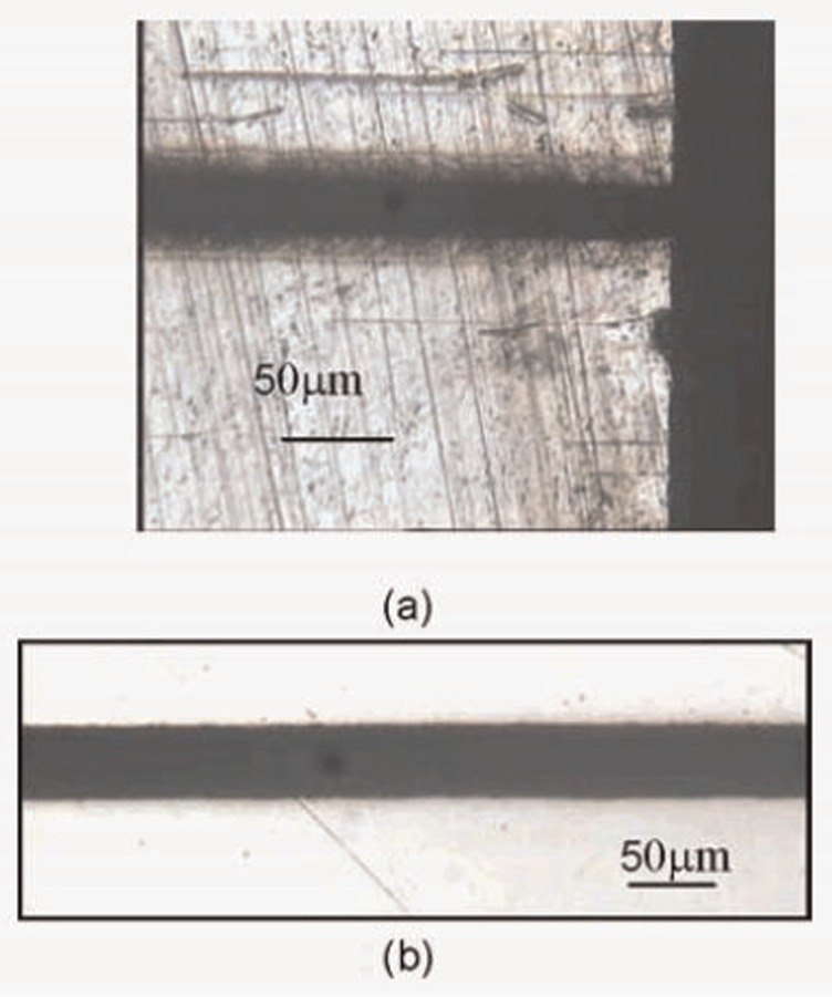
With the advent of high-precision machining, mechanical microcutting has emerged as a key technology for creating microchannels. The mechanical microcutting process is particularly suitable for fabricating individual personalized components rather than large batch size, which is largely indispensable for the current market situations. With high level of machining accuracy of ultra-precision machine tools, good surface finish and form accuracy can be achieved. The high machining speed of microcutting is another advantage over micro manufacturing technologies. Moreover, it can fabricate a large number of materials, such as steel, aluminum, brass, plastics and polymers. Unlike micro-laser beam machining and lithographic techniques, it does not require a very expensive setup, which enables the fabrication of miniatures at an economically reasonable cost. 53 Micromilling and micro turning are the two most used mechanical cutting processes. Recently, multicutter-based micromilling process has been studied 54 and found to be more economic and faster when compared to other contemporary micromachining processes. Figure 1 shows the microchannels machined using multicutter milling machine. In this process, composite cutting tool has been used and the depths of the microchannels were found to have inconsistency in depth. Also, it has been observed that the corners were not sharp instead curved which may result in creating void during sealing or bonding process. Microchannels have also been slotted on stainless steel using thin slotting cutters and top burr height was found to be predominantly controlled by feed and cutting speed, and the top burr width was strongly influenced by cutting depth, feed and cutting speed. 55 The significant disadvantages of mechanical cutting processes are wear of cutting tool, generation of cracks due to mechanical stress and long processing time.
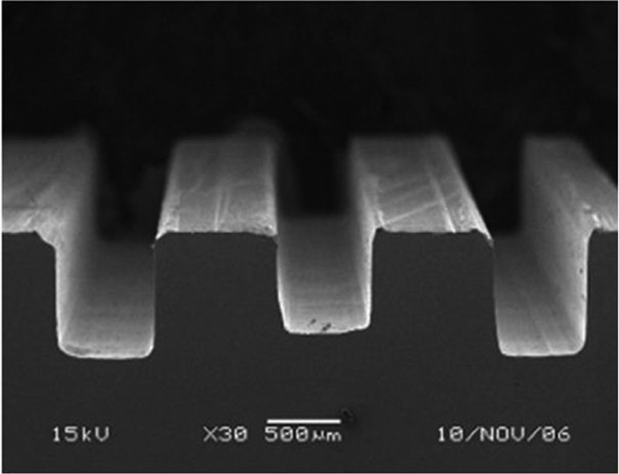
Multicutter milled microchannels.
Wet and dry etching
Etching is the most widely used subtractive technique for micromachining. Etching can be described as pattern transfer by chemical/physical removal of material from a substrate, often in a pattern defined by a protective mask layer such as a resist or an oxide. 56 In dry etching, surface is etched in the gas or vapor phase, physically by ion bombardment, chemically by a chemical reaction through a reactive species at the surface or by combined physical or chemical mechanisms. Sometimes a combination of wet and dry etching has also been used as a tool for micromachining. 57 Wet etching technique results in non-parallel walls on glass surface and as the channel etches deeper, the walls are also etched. Electrochemical etching in any acid/solution is dependent on etchant concentration as well as etching time. 58 Alternatively, dry etching techniques such as powder blasting 59 and plasma or deep reactive ion etching 60 have been proved to be much more effective technique than wet etching. Synchrotron radiation stimulated etching has been performed on a PDMS base material to etch patterns having lateral dimensions as precise as 21–24 µm and 32–35 µm by varying pattern mask sizes. 2 Etching is also used as a secondary process in various microchannel fabrication methods. 61
Wet chemical etching has been found to be suitable for metallic substrates that react well with chemicals. Dry etching has been mostly utilized for glass and polymer base materials due to requirements of lower reactive energy. 56
Lithography
Lithography is one of the major fabrication techniques used to fabricate microchannels. Lithography enables to fabricate many different types of topography which is hard to be generated using other fabrication techniques. Yao et al. 1 demonstrated a simple lithography technique to fabricate microchannels using simple processing steps as spin coating, baking, exposing and development. They fabricated the precise microchannels of different cross sections having dimensions of 10 µm × 7 µm × 200 µm and 4 µm × 1.8 µm × 1200 µm.
The most widely used form of lithography is photolithography. In the microchannel fabricating industries, pattern transfer from mask onto thin films is done majorly by photolithography. Lithography-based simple approach has been adopted by Abdelgawad et al. 9 for fabricating circular microchannels on PDMS of various diameters ranging from 5 to 200 µm in diameter. Pal and Sato 62 developed and demonstrated a fabrication method for various shapes of microfluidic channels and microstructures in one-step photolithography. Soft lithography has been used to create microchannels on PDMS. In this process, PDMS is cured over a patterned photoresist on the surface of a silicon wafer. 63 The cured PDMS is then removed and then joined to a glass surface to create closed microchannels. A significant benefit of using this fabrication technique is that the polymers can be easily bonded to each other or to glass or plastic substrate using conformal contact. 8 Disadvantages using soft lithography based on PDMS include the following: (1) shrinkage during cutting ranges to more than 1% and swelling also takes place due to nonpolar solvents such as toluene and hexane, (2) softness of the substrate material limits the achievable aspect ratio through sagging and (3) deformation of the soft elastomeric stamps. 64
In recent times, X-ray lithography has also been used to create polymer microchannels. 65 In contrast with ion-beam lithography and electron beam lithography, X-ray lithography does not require the presence of vacuum and clean room facilities, which makes this process cheaper and faster. 66 The majority of PDMS-based microchannels have been widely fabricated using this process. 67 PMMA absorbs most of the X-rays and is therefore best suited to be manufactured using this method. This process can produce high aspect ratio microchannels in PMMA. 8
Microchannel-based devices often possess requirements with respect to materials, geometry, aspect ratio, dimensions, shape, accuracy of microstructures and number of parts that cannot be fulfilled by mainstream machining processes. LIGA (German abbreviation for Lithography, Galvanoformung (electroplating) and Abformung (Molding)) enables the precise manufacturing of high aspect ratio microchannels ranging from 100–1000 µm. 53 LIGA exploits all the advantages of X-ray lithography. It involves high-energy X-rays and galvanizing techniques to fill the mold by a metal. LIGA enables new building materials and a wider dynamic range of dimensions and shapes.
Embossing and imprinting
For the first time, embossing technique for replicating microstructures was applied in the Institute for Microstructure technology of Forschungszentrum Karlsruhe during 1990s as a secondary process of LIGA. 68 In the course of due time, this technique has been developed to be independent technique for microfeature fabrication. The embossing technology that is particularly useful in replication process generally involves high degree of temperature equivalent to polymer molding temperature and therefore called hot embossing.
For imprinting on plastic substrates, wires are also used. In recent studies, silicon stamp has been found to be better imprinting tool for the fabrication of microchannel-based devices. A drawing of the channels using a computer-aided design (CAD) tool is replicated to a photomask for fabricating silicon stamp. If the required features have sizes more than 20 µm, a high-contrast resolution transparency is used instead of photomask. 69 A silicon micromachined wafer can also be used to create stamp out of metal. 70 A metal electroform, made of nickel, is produced using micromachined silicon wafer as the master. The first electroform will be a mirror image of the master, while the second electroform will be replica of the original master.
To fabricate a microchannel by using either embossing or imprinting, generally a cleaned plastic material is dried and placed over the silicon stamp or metal stamp. The embossing load, temperature and embossing time significantly affect the accuracy of microchannel width and depth. 71 The plastic material along with the stamp is then placed in a hydraulic press and a force is applied for sometime typically less than 10 min. Imprinting can also be carried out at room temperature and very high mechanical pressure or vice versa, that is, at high temperature and low mechanical pressure. Imprinting at very high pressure significantly reduces the fabrication time and also increases the life of substrate material. 72 However, when imprinting at very high pressure, the microchannel characteristics are dependent on parameters such as pressure, contact time and room temperature. Many common plastics have been successfully imprinted or hot embossed with excellent device-to-device reproducibility. These include PS, PETG, PMMA, PVC and PC. 65
Injection molding
Injection molding as a technique for fabricating microstructures was developed due to the low fabrication cost and the associated molding technique is called as micromolding technique. Micromolding technique is also called precision molding technique because of its high-precision output. 73 The injection unit of micro injection molding machine consists of various sub-devices such as heater, injection piston, shut-off valve, extrusion screw, dosing sleeve, nozzles and sprues. 74
Injection molding, which was developed for the fabrication of macro-, medium- and large-scale fabrication, has been adopted for the necessities of micro-component fabrication by different researchers. Researchers at ACLARA (ACLARA Biosciences Inc, CA, USA) were the first to use injection molding technique for fabricating microchannels. 70 In the injection process, the chosen polymer is required to have low viscosity and good contact with the mold walls to produce well-defined features. The parameters that affect the quality of microchannels in injection molding process include mold temperature and relaxation of polymer after release. By suitably adjusting and optimizing the processing time, temperature and relaxation behavior of polymer, the microchannel parts can be produced with high precision. Injection molding has been used to produce microchannels out of different polymers such as PC 75 and PMMA. 70 The major disadvantage of injection molding is the presence of weld lines in the fabrication of complex parts. Weld lines occur as the mold gets filled. The presence of weld line causes reduction in strength of macro 76 as well as micro parts. 77 The foremost advantage of using injection molding process when compared to imprinting or hot embossing is that preformed elements can be embedded into plastic during the process. 8 Matteucci et al. 78 utilized the method for fabricating multi-level microfluidic chips by means of silicon dry etching, electroplating and injection molding for applications in the fields of electrochemistry, cell trapping and DNA elongation. The chips ranged in sizes of channel depths between 100 nm and 100 µm and depth-to-width aspect ratios ranged between 1/200 and 2.
Other methods
There are various other techniques that have been developed over the years by different researchers but not widely available in the literatures. Guerin et al. 79 used SU-8 photoresist for realization of high aspect ratio microchannels to be used in thermal flow sensors using Mask and Fill process. Papautsky et al. 80 fabricated microchannels of different dimensions on top of silicon and glass substrates. The length of these microchannels ranged from 0.5 to 12.75 mm and width from 20 µm to 1.5 mm. The height of the microchannel varied from 5 to 100 µm. At this low temperature (<110 °C), IC-compatible process for fabrication of metallic microchannels uses a variety of electroformed metals. This process involves spin coating of the molding wall in addition to standard lithography technique. Electrospinning has also been used by Vempati and Natarajan 81 to create polymer microtubes and microchannels. In their method, they have the technique to selectively wash the electrospun fiber. Noh et al. 82 presented the idea of fabricating parylene microchannels using micromolding technique. This method consists of Si mold fabrication and then parylene deposition on Si mold and stainless steel sheet. It also involves thermal bonding of two parylene deposits. Lin et al. 83 described a low-cost and fast prototyping process for fabrication of microfluidic channels on soda-lime glasses. In this method, they used AZ4620 positive photoresist instead of expensive polysilicon nitride layer as an etch mask which avoids serious peeling problems. A microfluidic channel with a depth of 35.95 ± 0.39 µm is formed after 40 min buffered oxide etching (BOE) in an ultrasonic bath. The resulting channel has a smooth profile with a surface roughness of less than 45.95 ± 7.96 Å. Kee et al. 51 fabricated ceramic-based micro-heat exchanger based on microchannels using PLIS method. In this method, ceramic powders are mixed with appropriate binders and microchannels are formed using hydraulic press. Although the channel has inconsistency in depth, the process appears to be very simple and cost-effective. Hakamada et al. 84 fabricated microchannels on copper substrates using spacer method. In this method, pores of the size of micrometers are obtained, by the removal of spacers, without bonding. Substitution of strings with a diameter of the order of micrometers for the spacer particles may make it possible to fabricate microchannel structures in metal bodies. Lee et al. 85 described the use of low-energy ion-beam etching to fabricate high aspect ratio microchannels in number of fluoropolymers including polytetrafluoroethylene (PTFE), Teflon®, Tefzel® and fluoroethylenepropylene (FEP). Plasma etching has been used for creating microchannels in polymer substrates by Rossier et al. 86
Laser-evolved microchanneling
As far as process complexity is concerned, laser-associated microchannel fabrication processes are most simple in nature with capability of generating almost every shape of microstructures. Laser processing is very versatile, takes minimum amount of time and can be used on almost every type of substrate material. In most of the cases, the material removal phenomenon is heat dependent; the processing must be optimized for getting the best possible result. Laser processing of microchannels has evolved recently and has been studied by different researchers. In most of the researches, either neodymium-doped yttrium aluminum garnet (Nd:YAG)4,87 or excimer laser 88 has been used. A few researchers have also used CO2 lasers for fabricating microchannels. 89 Most of the laser fabricating processes involve either one or maximum two steps only; they do not require clean room facilities. They do not require the preparation of mask, such as in photolithographic process or etching process. There are numerous advantages of using lasers as microchanneling tool over other processes. Laser-based processes are environmentally clean, scrapless and based on simple-to-operate techniques. With the use of appropriate kind of laser, almost every kind of material including metals, nonmetals and ceramic can easily be cut into almost any shape. It also covers a wide range of operations such as drilling, engraving, scribing, joining, microstructuring and surface modification which can be used to fabricate the whole device in its entirety. 35
In the most basic sense, material ablation phenomenon is caused by a laser beam striking the surface. The energy of the photons in laser beams varies depending on the wavelength of the laser. While the photons of shorter wavelength laser contain higher amount of energy, the photons of higher wavelength contain lower amount of energy. This is one of the reasons that shorter wavelength laser beams are in greater use than higher wavelength laser beam since they can be utilized to cut transparent materials such as glass and quartz. The shorter UV wavelength (193, 266, 355 nm) laser beams are found to be more suitable for ablation of Si or SiO2 than longer infrared (IR) wavelength (usually 1064 nm) laser beams from the study of absorption coefficient of these materials. 90 However, thin SiO2 films also possess a good degree of absorption at 10 µm wavelength and had been studied by various authors. 91 Recently, microfabrication using laser-assisted photopolymerization technique has enabled the microfeatures as small as 120 nm on urethane acrylate monomer. 92
In the market, there are different kinds of laser sources available producing wavelengths ranging from deep UV (157 nm) to IR (10 µm) and pulse durations from microseconds to femtoseconds.
UV laser microchanneling
Excimer lasers and higher harmonics Nd:YAG laser are the most used UV laser micromachining devices. Although the fundamental wavelength of Nd:YAG laser is 1064 nm, the wavelength can be varied using harmonic generators. Since the photons of UV lasers carry very high energy, the material ablation takes place by means of electronic excitations which causes the ionization by breaking chemical bonds between the atoms. In most of the cases, the thermal damages such as HAZ, burrs and redeposition of ablated material get reduced considerably. This kind of material removal phenomenon is termed as cold ablation or photoablation. 93 However, in actual practice the material removal phenomenon has been found to be composed of photoablation as well as thermal ablation depending on the material type. Most of the polymers undergo photoablation as well as thermal ablation. 94
UV lasers require specially designed optics, beam delivery and diagnosis. Excimer lasers often require mask to produce microchannels in order to selectively etch the surface. 95 Most of the UV lasers and excimer lasers have been specially used for polymeric material. Most of the polymeric materials are extremely heat sensitive. The UV laser has higher absorption and lower HAZ than lasers of higher wavelength.
Many researchers have used UV laser micromachining technique to create microchannels. Heng et al. 88 fabricated microfluidic channels on 1.5-mm-thick PMMA using 248-nm excimer laser direct writing technique and evaluated the effect of laser fluence on depth and surface roughness of the channel. They concluded that higher laser fluence increases both the channel depth and surface roughness and therefore must be optimized. For enhancing the surface roughness, excimer laser polishing has been applied and found that if irradiation time exceeds to certain threshold value of time, the tenuous stripes appear to begin on the surface resulting in poorer surface finish. Yu et al. 96 utilized a third harmonic Nd:YAG lasers (355 nm) for rapid processing of freeform multilayered microstructure. They realized UV laser–assisted lithography technique for the processing of photosensitive polymer such as SU-8. Kitsara et al. 97 also utilized the UV-based lithography for fabrication of microchannels on epoxy-based resists. Fernandez-Pradas et al. 49 utilized the third harmonic Nd:YAG laser (355 nm) for successfully fabricating the microchannels on photostructurable glass ceramic. They also performed thermal treatment process and chemical etching after the laser ablation process. Waddell et al. 34 used a pulsed KrF excimer laser of 248 nm wavelength and pulse duration of 7 ns in different atmospheric conditions to create microchannels on PMMA substrates. It has been found that the surface morphology of the ablated region is dependent on the temporal profile, the spatial profile and the wavelength of the laser pulse. The longer the laser pulse duration, the greater the fluence required to ablate the substrate. This is because the ablation of the surface is a function of the energy deposited per unit time. 98 Cycloolefin copolymer (COC) microchannels were fabricated by Sabbert et al. 99 using ArF excimer laser (193 nm).
IR laser microchanneling
Nd:YAG lasers, fiber lasers and CO2 lasers are most widely used lasers in this category. Most often the original wavelength of Nd:YAG laser in IR range is 1064 nm and CO2 laser falls in the category of mid-IR range having wavelength of 10640 nm. Lasers belonging to 1064 nm wavelength such as Nd:YAG and fiber lasers are especially suitable for metallic components and generally used with metals and semiconductors. However, CO2 laser (10,640 nm) has been found to be mostly used with polymers and organic materials because of its better absorptivity with such materials.
Microchannel with flat wall and herringbone ridges on 660 µm thick silicon was fabricated by Lim et al. 87 They fabricated multiple-level microchannels having constant depth of 125 µm and widths of 250, 200, 160 and 125 µm using a high brightness diode-pumped Nd:YAG laser. The whole operation was carried out in open air without the use of assisting gases. Hong et al. 89 used high-speed CO2 laser built for scribing purpose in fabricating PMMA-based microfluidic devices using unfocused laser beam (Figure 2). Karazi et al. 100 fabricated internal microchannels on PMMA using Nd:YVO4 laser and concluded that micromachining cost is inversely proportional to translation speed and plays a major role in determining the operating cost while laser power as well as pulse repetition frequency also play a significant role in determining operation cost. Kam and Majumder 95 used a Q-switched Nd:YAG laser for fabricating microchannels on silicon for biomedical applications. After the process, to clean up the debris chemical etching process has been applied using hydrogen fluoride (HF) and nitric acid (HNO3).
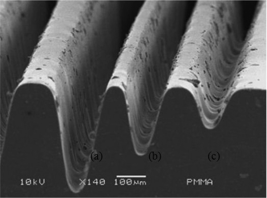
SEM image of PMMA substrate with channels of different depths produced by unfocused laser beam (k = 20 mm) with constant laser power of 4 W and scanning speeds of (a) 80 mm/s, (b) 120 mm/s and (c) 150 mm/s, respectively.
In a recent research at Technical University of Denmark (DTU), 101 CO2 laser has been used to fabricate microfluidic structures on PMMA substrates. The ablated channel depth was between 100 and 300 µm and width was around 250 µm. The surface roughness was found to be around 1–2 µm. They also suggested that surface roughness and rugged appearance could have been improved by thermal annealing without altering the channel shape; the advantage of having smooth surface is that it minimizes the light scattering phenomenon helping in optical detection process in microfluidic channels. Apart from PMMA, PC has also been used, 102 to fabricate low-cost disposable devices using a CO2 laser. Cheng et al. 103 experimented on PMMA with varying aspect ratios of microchannels. The widths of microchannel varied from 100 to 900 µm and the aspect ratio to be kept around 7. They stated that around thousands of devices can be produced in a day using one system, and therefore mass production can be done easily without investing big amounts of money.
Microchanneling by short and ultrashort pulse laser
With the advent of femtosecond lasers, the cut quality characteristics of microchannels have been much improved. As the pulse duration is extremely small, the peak power of more than 15 GW can be reached. 104 When the intensity of the pulse incident on a target exceeds 1013 W/cm2, the ablation process enters a new regime that is no longer initiated by the presence of a very small number (e.g. 0, 1, 2) of free electrons trapped in defects and impurities within the ablation zone. 105 Instead, it starts from a large bath of valance electrons stripped off atoms via Zener tunneling (this is not multiphoton ionization (MPI)). 106 At such a small pulsewidth, the nonlinear absorption of the material becomes important for every material whether it is opaque or transparent to the associated wavelength of the laser.
The material ablation is the result of combination of two kinds of phenomenon thermal vaporization and Coulomb explosion depending on laser wavelength, pulse duration and number of pulses. 107 Coulomb explosion is a way of gentle ablation which occurs at near-threshold pulse energy and produces very fine surface quality with approximately no evidence of melt zone. In this phenomenon, the high-energy ultrashort pulses evacuate the electrons from the workpiece, and therefore a region of positively charged ions is formed. Due to these positively charged ions, the ejection of the near surface layer takes place due to electrostatic repulsion. Coulomb explosion takes place when pulsewidth ranges between 10 ps and 10 fs. 93 Coulomb explosion has found to be specially dominating in initial stages. However, after a certain time gap, the material removal phenomenon becomes dominated by thermal vaporization. The thermal vaporization phenomenon is found to be more dominant when the number of pulses is more. 108 Of the three main kinds of material, that is, semiconductor, metals and dielectrics, the material removal process in dielectrics is mainly dominated by Coulomb explosion phenomenon. However, it is not a major factor in metals and semiconductors. 109 The exact physics behind material removal in femtosecond lasers is still pretty complex and varies with material to material as well as change in parameters. 110
The vibrational modes, or phonons, of a material (the mechanism by which heat diffuses) take a finite amount of time to build up. Femtosecond pulses engage materials as true impulses in the sense that the material cannot respond fast enough to diffuse appreciable heat. After the ionization saturates, hydrodynamic expansion of the plasma (material ejection) carries away nearly 100% of the initial laser energy. Nothing is left to heat the surrounding material.
Femtosecond laser processing has proved to be the most efficient and successful technique to create microchannels as far as repeatability of dimensions and quality of microchannels is concerned. The fabricated microchannels are found to be HAZ free, free from thermal cracks and remain clog-free. 107 Using femtosecond laser processing, an optical circuit structure can be directly printed and fabricated on optically transparent materials. It is also possible to build 3D structures. 111 Day and Gu 112 fabricated a PMMA microchannel of circular cross section using femtosecond laser pulses having pulse duration of 80 fs having diameter ranging from 8 to 20 µm. After the laser machining, the samples were annealed on a hotplate above the glass transition temperature of the material. Nakashima et al. 48 fabricated 3D hollow microchannels on gallium nitride (GaN) using a femtosecond laser. They etched the microchannels in wet as well as dry conditions. They fabricated craters as small as 510 nm. Maselli et al. 61 also fabricated the circular microchannels in fused silica using femtosecond laser having astigmatically shaped beam and chemical etching. Kuršelis et al. 113 studied the phenomenon of femtosecond laser micromachining of grooves in stainless steel. Farson et al. 3 fabricated internal microchannels on PMMA for use in biomedical devices. They carried out the experiments to successfully fabricate the clog-free microchannels having diameter sizes ranging from 2 to 20 µm and lengths of 12 mm. The femtosecond laser irradiation can be improved by following a chemical etching (Femtosecond laser irradiation followed by chemical etching; FLICE) technology; however, this fabricating process is accompanied with extra access structure that may have side effects on microdevices’ function or microfluidic performance. 114
Laser microchanneling in different environments
Over the years, various kinds of laser processing have been studied. Laser processing under different environments has always been a point of continuous discussion in recent researches. Various kinds of assisting gases use to help in removal of redepository materials on the surface as well as to reduce the HAZ and sputtering. Apart from gases, liquids including different chemicals and water have also been studied by some researchers. Plasma and shock waves are formed near the target surface in high-intensity laser processing in a gas environment. The material removal takes place due to optical breakdown. 115 However, material removal phenomenon under liquid is quite different and complex. The liquid limits the expansion of plasmas around the target surface, and therefore the pressure induced due to recoil pressure increases manifold. The bubbles are formed continuously by the formed plasmas which affect the entire target surface. When the target is immersed in a liquid medium, the incompressible liquid limits laser plasma to expand externally and thereby recoil pressure caused by the shock wave of plasma increases toward the target. 116
A few researchers investigated the laser fabrication process with different environments during the material ablation process while a few have used the environment after the process in order to create clean, clog-free 3D structures. Laser processing in underwater condition was first studied by Ageev 117 to study the material ablation phenomenon during emission spectroscopy. The use of underwater processing has eliminated the use of workpiece after cleaning which is generally done by ultrasonic bath. 118 During the laser ablation process, the debris is carried away due to thermal convection and bubble movements during the process. However, this effect is visible only when the laser pulse duration is short, that is, nanoseconds and femtoseconds. If the pulse duration is larger than 100 µs, the debris are not eliminated. 119 Laser lights having wavelength in the green region (532 nm) are most transparent to water. The light, when processed through water, ablates the material via vaporization and plasma formation. 120 Choo et al. 121 compared the excimer laser micromachining phenomenon in air and under water for silicon wafers. They observed the absence of thermal damage in case of underwater micromachining while significant amount of thermal damage has been observed in case of open air machining. The presence of liquid layer carries away the debris and acts as a cooling agent minimizing the HAZ and molten material. Figure 3 shows the difference in quality of microchannels etched on PMMA by direct laser ablation in the water and open air. The width as well as the depth of the channel were kept around 300 µm to suit the requirement of the number of microfluidic devices. From the figure, it can be concluded that in the presence of water, the cut quality characteristics are much more improved than in open air. It leads to significant reduction in burr formation and HAZ on the surface of the substrate. The water level has been kept at 1 mm during the experiment. 4 In this research, Nd:YAG laser having 1064 nm wavelength has been used and the material thickness has been taken as 4 mm, usually suitable for biomedical applications.
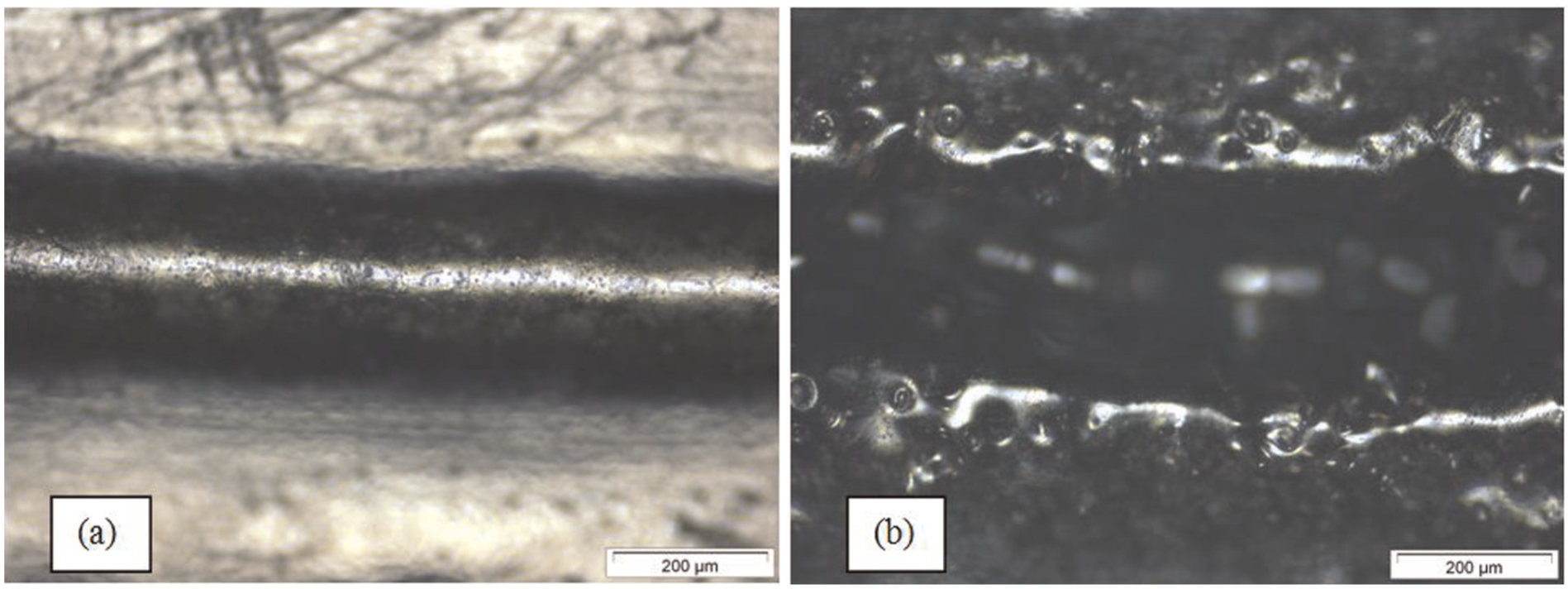
Microscopic view of microchannels created in (a) underwater processing and (b) open air processing. 4
Microdrilling on Pyrex® glasses are crucial for microfluidic devices. High aspect ratio holes were drilled and studied by Chung and Lin. 122 The liquid-assisted laser drilling has found to be free from cracks and scorches. Water-assisted laser processing has been specially suited for continuous wave lasers such as CO2 where the material ablation phenomenon is purely thermal in nature. Muhammad et al. 123 compared the wet and dry fiber laser profile cutting of 316L stainless steel tubes having 200 µm wall thickness and 4 mm diameter. Wet cutting resulted in zero back wall damage of the tubes which is a major problem in open air processing. They further reported the absence of dross and HAZ in wet laser processing. Water has been used as a cooling media. Wee et al. 124 conducted micromachining test on silicon wafer to be used in electronic and biomedical devices. The experiments were carried out in open air and under flowing water conditions using 355 nm AVIA-X laser (Figure 4). Underwater drilling has been proved to produce less taper in holes than in open air drilling because of efficient material removal in the presence of water. However, the surface irradiated in case of open air has been found to be smoother than in underwater conditions possibly because of trapping of plasma into water and bubbles which further ablates the surface of the target material. The flowing water augments the ablation efficiency and produces spatter free holes. It has also been observed that ablated materials get redeposited at the points where bubbles have been formed. The presence of inflowing water has also found to increase the ablation rate by decreasing the beam blocking elements and removing material redeposition during simultaneous drilling on soda-lime glass in femtosecond laser ablation. 125 Underwater micromachining of thin nitinol sheet has been carried out by Muhammad and Li 126 using Ti:sapphire, 800 nm laser of 100 fs pulsewidth. The resulting surface has been found to be free from spatters, HAZ, debris and burrs around the cutting surface.
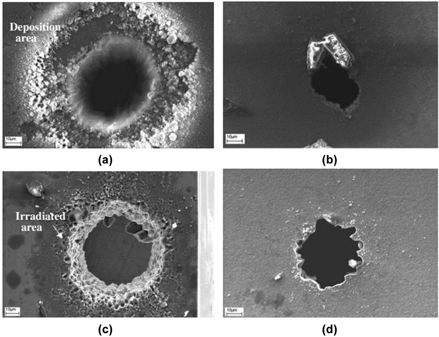
Entrance and exit holes for air and water drilling at a scan speed of 0.5 mm/s: (a) entrance hole, (b) exit hole in air drilling, (c) entrance hole and (d) exit hole under water drilling.
Chang and Molian 25 investigated PMMA, PE and PP micromachining using excimer laser of 193 nm to compare the open air machining, in ethanol and methyl alcohol. In PP and PE, the material removal takes place layer by layer by maintaining homogeneity. The PMMA etches faster in the presence of methanol and ethyl alcohol. Li and Achara 127 used the salt solution as a cutting environment media for stainless steel. With the use of salt solution, the material ablation rate has been improved by 300%. The cut quality characteristics have also been improved by reduction in the HAZ and recast layers around the microchannels (Figure 5). Nakashima et al., 48 at Riken, Japan, used the hydrochloric acid (HCl) solution as a cooling media in etching the single-crystal GaN by a femtosecond laser. They also made a comparison of the process in which the GaN was etched in HCl solution under femtosecond laser processing to a two-step wet chemical etching–assisted laser micromachining process. They concluded that the two-step process in which first the femtosecond laser beam has been utilized in open air and then the substrate is etched in HCl solution results in improper shape. While the machining in HCl environment results in high-quality ablation, the shape gets distorted in two-step etching process. Saponification as a chemical treatment has been used to increase the electroosmotic flow and carboxylate ions inside the PET microchannels to be used for DNA analysis. 128 Kam and Majumder 95 studied the effects of inert gas (argon) during fabrication of microfluidic process on silicon wafers. Argon, being an inert gas, improves the surface quality by effectively removing the molten material out of microchannels. Channel quality was further enhanced by performing wet chemical etching process using HF and HNO3 as chemical etchants.
Comparison of laser-machined grooves in (a) open air and (b) salt solution.
Future trend and research issues
Fabricating microchannels on different materials is a challenging task. To meet required precision in geometry of microchannels, a considerable amount of research is needed. The use of microchannels in various devices has brought a revolution in terms of cost, innovation and efficiency. This allows the easy portability of device and to build many devices on a single platform (lab on a chip). Therefore, a significant amount of research is needed to develop the microchannel fabricating techniques in most efficient way. A summary of all the above-discussed methods has been provided in Tables 1 and 2 depending on the kinds of application, materials, advantages and disadvantages.
Summary of microchannel fabrication methods with their advantages and disadvantages.
Summary of laser-evolved microchannel fabrication methods with their advantages and disadvantages.
UV: ultraviolet; IR: infrared; PMMA: polymethyl methacrylate.
Microchannels have been fabricated on different types of substrates over the years. Polymers top the list as far as most wide use is concerned. However, fabricating microchannels on polymers has always been a tough task for manufacturers because of its brittle nature and uncontrolled fracture. Metals on the other hand does not offer all the required properties such as nonreactive nature and optical transparency, therefore, cannot be used in all the applications though fabricating microchannels on metals is considered to be easier than polymers. Since silicon has a very high thermal conductivity, any thermal-based fabrication process does not specially suit the sensitive devices because the absorbed heat reduces its sensitivity. Some authors have also studied the ceramics and semiconductor materials, but the higher input costs associated with these materials restrict their usage. Therefore, significant amount of research is required to develop materials which are cost-effective and easier to fabricate. This will enable the innovations to take place at a faster pace.
Fabricating microchannels using conventional technologies such as photolithography and etching takes a lot of time and often restricts the production of microchannel-based devices en masse. The difficulty in these processes also limits the flexibility and size of fabrication. Multiple steps, alignments and exposure make these processes costlier and time-consuming. With the advent of maskless photolithography process 129 the required time consumption has been reduced, but the process has not been automatized fully and successful fabrication depends on manufacturer’s skills and experience. Again in most of the lithography-based processes, there is always a need to do post-processing such as wet etching and other chemical treatments in order to fabricate channels of high resolutions, which further add to the cost of fabrication. Embossing and imprinting processes require the need of replicating the microfeatures on a stamp which gradually wears out resulting in improper channel dimensions. Further fabricating these replicating devices requires the need of photolithography which again increases the cost of manufacture to manifold. Different other types of hybrid fabrication technologies have been used by different researchers. However, the lack of standardization of these processes does not make them a manufacturer’s first choice. Further significant development is required in order to achieve the required precision.
Microchannel fabrication using laser is a recent trend and offers solution to many problems. The ease of fabrication, minimum time consumption and cheapness of the process make it the most preferred choice. However, the damages occurring due to its thermal nature cannot be ignored. Sometimes, the surface gets damaged in an undefined manner so that it cannot be used for the purpose it was built for. Burr formations and HAZ also limit the use of lasers in fabricating microchannels. Therefore, process parameters must be optimized in order to get quality microchannels. Furthermore, a lot of research is needed to reduce the thermal surface damage by altering the process or by using some post-processing. The use of mechanical cutting processes such as micromilling is also gaining reputation in the area of microdevice manufacturing because of its ability to cut any material that can be machined. Furthermore, the energy consumption of such processes is much less when compared to other nonconventional processes. In spite of several advantages associated with mechanical cutting processes, the micromilling approach is not fully understood and there is minimum experience pool in industry for its introduction. 130
Footnotes
Declaration of conflicting interests
The authors declare that there is no conflict of interest.
Funding
The authors acknowledge the financial support of the Department of Science and Technology, Government of India, for providing INSPIRE fellowship to one of the authors for pursuing research.