
Abstract
In this study, a study has been conducted on fabrication and control of different grain sizes of micro features fabricated by ultrasonic-assisted jet electrodeposition process using pulsed current power supply. At the present time, grain sizes have been controlled to improve the mechanical properties of fabricated micro features. The centre of attention of the study is application of pulsed power supply on the developed ultrasonic-assisted jet electrodeposition set-up, which involves pulsed current application between nozzle (electrolyte) and work surface in ultrasonic-assisted jet electrodeposition process instead of direct current application. The impacts of frequency and duty cycle on the grain size, nanomechanical properties and microhardness of fabricated micro features have been studied. It is experimentally observed that the pulsed current ultrasonic-assisted jet electrodeposition process has the capability to fabricate nano-sized grain micro parts and yields better mechanical properties as compared to those obtainable using direct current ultrasonic-assisted jet electrodeposition process.
Keywords
Introduction
Present-day requirements of modern world community have encouraged manufacturers to change from macro fabrication to micro fabrication. The modern developments in various sectors such as automobiles, aviation, space, electronics and computers (printed circuit boards), optics, biomedical and surgical (medical tools) instruments have forced reduction of instrument sizes. The strict controls for environmental issues with better reliability and design have also minimized the equipment size. There is a demand for metallic microstructures with relatively small thickness (i.e. 10–1000 µm). 1 This has resulted in greater need of suitable micro manufacturing techniques.
Chemical-based micro fabrication is one domain for manufacturing of micro features. Chemical-oriented processes have the competence to fabricate highly precise features/structures at comparative lower expenditure. 2 There are chemical-oriented conventional well-established processes such as LIGA (German acronym of lithography, electroplating and moulding) and photo-electroforming for micro manufacturing. 2 The current thinking in this direction is to combine the LIGA process with developments in surface micromachining to permit the fabrication of complex three-dimensional (3D) microstructures using a reliable process. 3 These processes are slow, costly and also involve hazardous chemicals for etching the masks during fabrication. 1 Vaezi et al. 4 have specified 3D micro-additive manufacturing techniques as a separate class of fabrication techniques for manufacturing of functional and 3D microcomponents/assemblies. They also classified 3D micro-additive manufacturing techniques into three groups: scalable micro-additive manufacturing systems, 3D direct writing and hybrid processes. Hybrid processes were further classified into two groups as electrochemical fabrication and shape deposition modelling. Under electrochemical-based fabrication techniques, in the recent times, high-speed selective jet electrodeposition (HSSJE) 5 and ultrasonic acoustic liquid manipulation–assisted electrodeposition (UALMAE) 1 are in the developmental stage for speedy, less expensive and less perilous fabrication method.
Selective jet electrodeposition was developed by Fletcher and Oliver 5 in 1972. This method was evolved to electroplate the substrate surface in particular chosen pattern. This method has been further developed as HSSJE to fabricate micro features by Dover et al. 6 and Kunieda et al. 7 HSSJE involves impingement of electrolyte jet in cathode surface. 6 Electrolyte jet was used to flow current by maintaining the voltage difference between nozzle opening and substrate. This resulted into deposition at the impingement region due to reduction of metal ions of electrolyte. The relative motion was maintained between work surface and impinged jet in a specific pattern to fabricate the feature through layer-by-layer deposition. 6
When ultrasonic vibration is given to fluid, it starts travelling through the fluid as ultrasonic sound waves of high frequency (above 20 kHz). 1 When these waves travel through the fluid or solid, amplitude of vibration reduced due to absorption of vibration energy by fluid. This absorbed energy resulted in streaming of fluid. The acoustic energy, when used to move liquid, manipulate liquid surfaces and propel buoyant objects, is known as acoustic liquid manipulation (ALM). 8 In electroplating, ALM was used by Gadkari and Nayfeh 1 for fabrication of micro features. The tank dipped electrodeposition process ceased to cause required deposition after some time of starting the process. This phenomenon took place due to the formation of thick ion-exhausted layer over workpiece, which resulted in reduced supply of metal ions needed for proper deposition. The small supply of metal ions at a very slow rate was also caused by diffusion. Gadkari and Nayfeh 1 and Oeftering and Denofrio 9 used ALM to inject streams of fresh ions from electrolyte to specific areas of workpiece and continued the electrodeposition process at a faster rate only in the focused regions.
HSSJE and UALMAE are two different chemical-based processes, having different principles of selective deposition. For the first time, these processes were combined and studied by Von Gutfeld et al. 10 as acoustic-assisted jet plating. Their process involved ultrasonic acoustic waves inside the jet. Their results showed improved morphology of deposited structure without significant impact on deposition rate. Rajput et al. 11 developed ultrasonic-assisted jet electrodeposition (UAJE) process for fabrication of micro features. UAJE process is a combination of HSSJE and UALMAE processes, in which ultrasonic vibrations are used to set up acoustic waves inside the jet and can be used for fabrication of better morphological and accurate micro parts/features. 11 Ultrasonic waves inside the jet create complicated non-linear interaction precisely upon the substrate, which causes homogeneous deposition all along impingement zone, and result in more homogeneous and dimensionally stable feature with the absence of edge effect. 11
Mechanical, tribological and chemical properties of micro features used in micro systems are very important for better performance of the part. It is evident that the nano range grain size significantly affects mechanical, physical and chemical properties. 12 Chemical-based processes involving electrodeposition have the capability to fabricate nano-sized grain products. Electrodeposition process with pulse current supply has been used to produce nanocrystalline metals, alloys and composites. 12 Therefore, pulse power supply may be used with UAJE process to get nano-sized grains in micro parts. This study focuses on the study of pulsed current supply UAJE process and properties of nanocrystalline micro features produced by this method. The scanning electron micrograph (SEM) images have been taken to study the grain size of micro parts. The nanomechanical property of these micro parts has been studied by plotting force–displacement diagram using atomic force microscopy (AFM) technique. AFM has also been done to study the surface unevenness. Microhardness has also been measured at different grain size depositions.
Pulsed current UAJE set-up fabrication and experimentation
In this work, nozzle assembly (shown in Figure 1) has been used to form an electrolyte jet. An ultrasonic horn is attached to one end of the nozzle assembly to transfer vibration to the electrolyte. The nozzle assembly has been utilized to develop experimental set-up for UAJE and pulsed current supply UAJE. A pulse power supply has been attached between nozzle opening and work surface. This section deals with details of nozzle assembly, experimental set-up with pulsed power supply, selection of process parameters and experimental procedure.
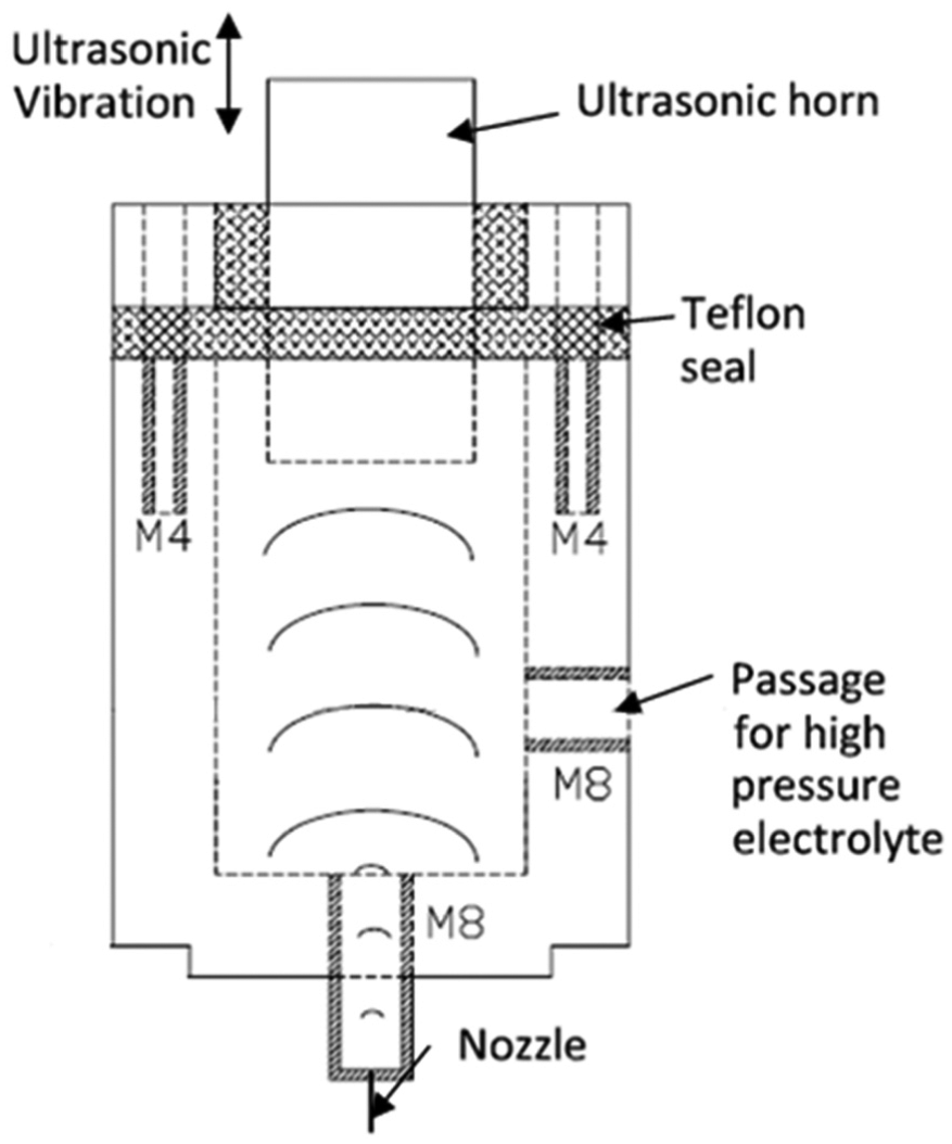
Block diagram of nozzle assembly.
Details of experimental set-up
The deposition, required to form the feature with jet electrodeposition process, is caused by the current flowing through jet. The current is produced by application of voltage across the jet (between nozzle and substrate) using a pulsed power source. The current flowing through electrolyte jet is a function of voltage, concentration of ions in electrolyte solution and inter electrode gap (gap between anode and cathode). The ultrasonic acoustic waves within the jet enhance uniform distribution of ions at deposition zone. These waves hit at deposition surface and are thrown back. The waves intermix with the new arriving waves as shown in Figure 2. These phenomena result into enhanced uniform deposition at impingement zone. 1
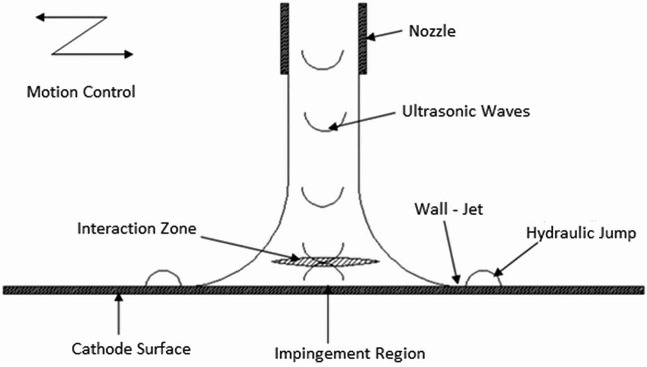
Schematic representation of the high-speed selective jet electrodeposition process with acoustic streaming.
The vibrations also cause pressure variation in its path and are being transferred to the nozzle opening and effect is being observed visually as change in jet speed and jet profile. This variation helps to achieve uniform deposition on substrate. Therefore, the nozzle has been used with ultrasonic horn, which is assembled, as shown in Figure 1. The nozzle is made up of stainless steel, which has three openings. In one opening, ultrasonic horn is fitted. The distance between vibrating surface of ultrasonic horn and nozzle opening was maintained at ∼75 mm. The other two openings are given for the flow of pressurized electrolyte. Electrolyte enters inside the nozzle from side opening of 4 mm diameter, placed at 15 mm below the vibrating surface of horn. The vibrating surface had 20 mm diameter and arranged coaxially (Figure 1) inside the electrolyte chamber of nozzle assembly of 30 mm diameter. Electrolyte comes out as jet from the other opening of 137 µm. The electrolyte jet is used to fabricate the feature by scanning the substrate. The details of ultrasonic vibration unit are given in Table 1.
Details of ultrasonic vibration generator unit.

The pulsed current to UAJE set-up has been supplied by a pulsed power supply (Model-SM5074; Make-Scientific Mes-Technik Pvt. Ltd, India, Indor-452015). The set-up mainly composed of an ultrasonic vibration generator unit, nozzle and substrate. Other components of set-up are electrolyte tank, compressor and 2.5-axis computer-controlled slides. The schematic diagram is shown in Figure 3 and the actual image of set-up is shown in Figure 4(a) and (b). Nozzle opening is attached to positive terminal of pulsed power supply to make it anode. Negative output is attached to workpiece (cathode). Output of compressor is attached to electrolyte tank. Electrolyte tank is connected to nozzle assembly for providing pressurized (2 bar) electrolyte. Substrate is held on the slides (x- and y-axis computer-controlled and z-axis manually operated). During the experimentation, only x–y slides were given motion and z-axis (gap between work surface and nozzle opening) was kept static.
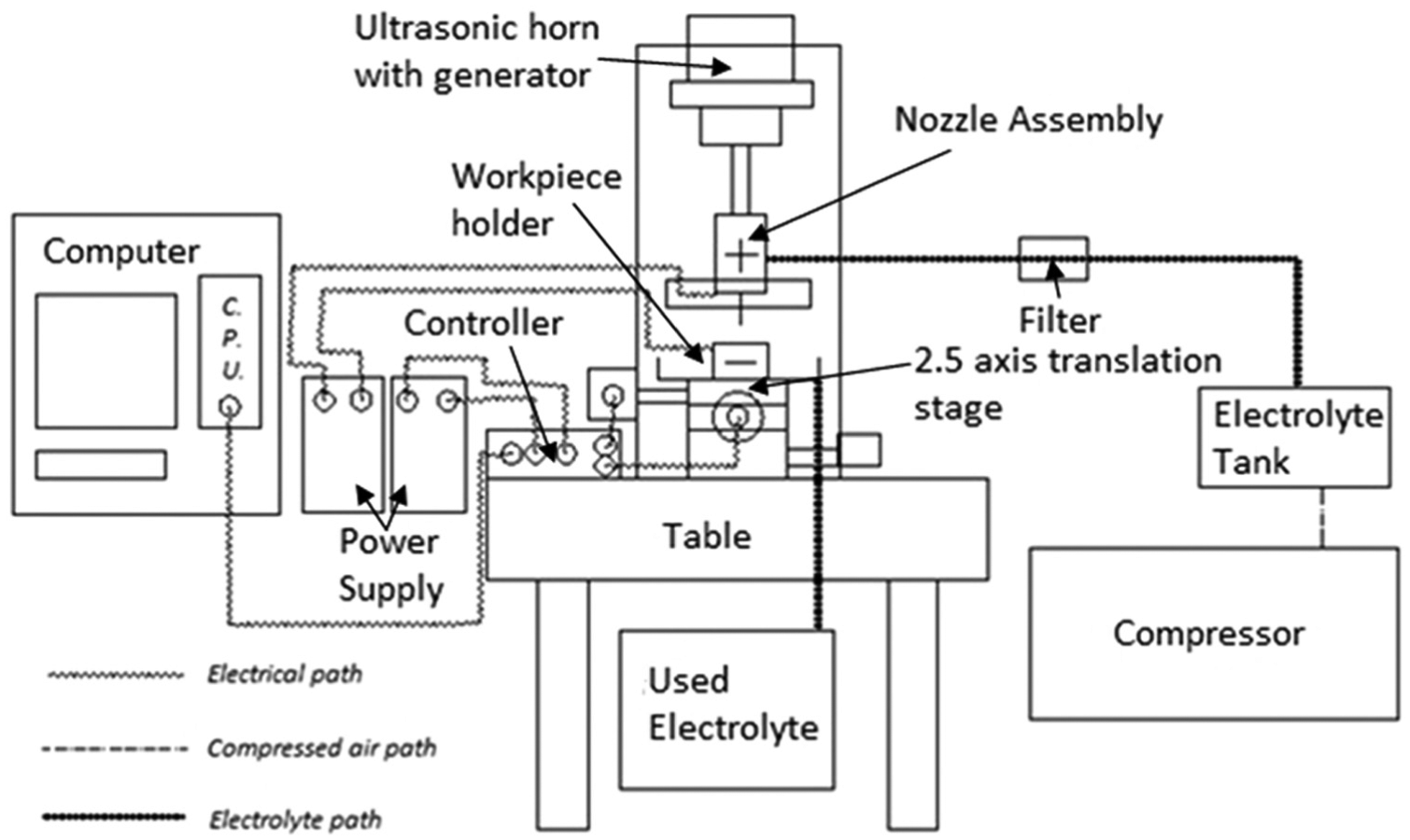
Schematic diagram of UAJE set-up.
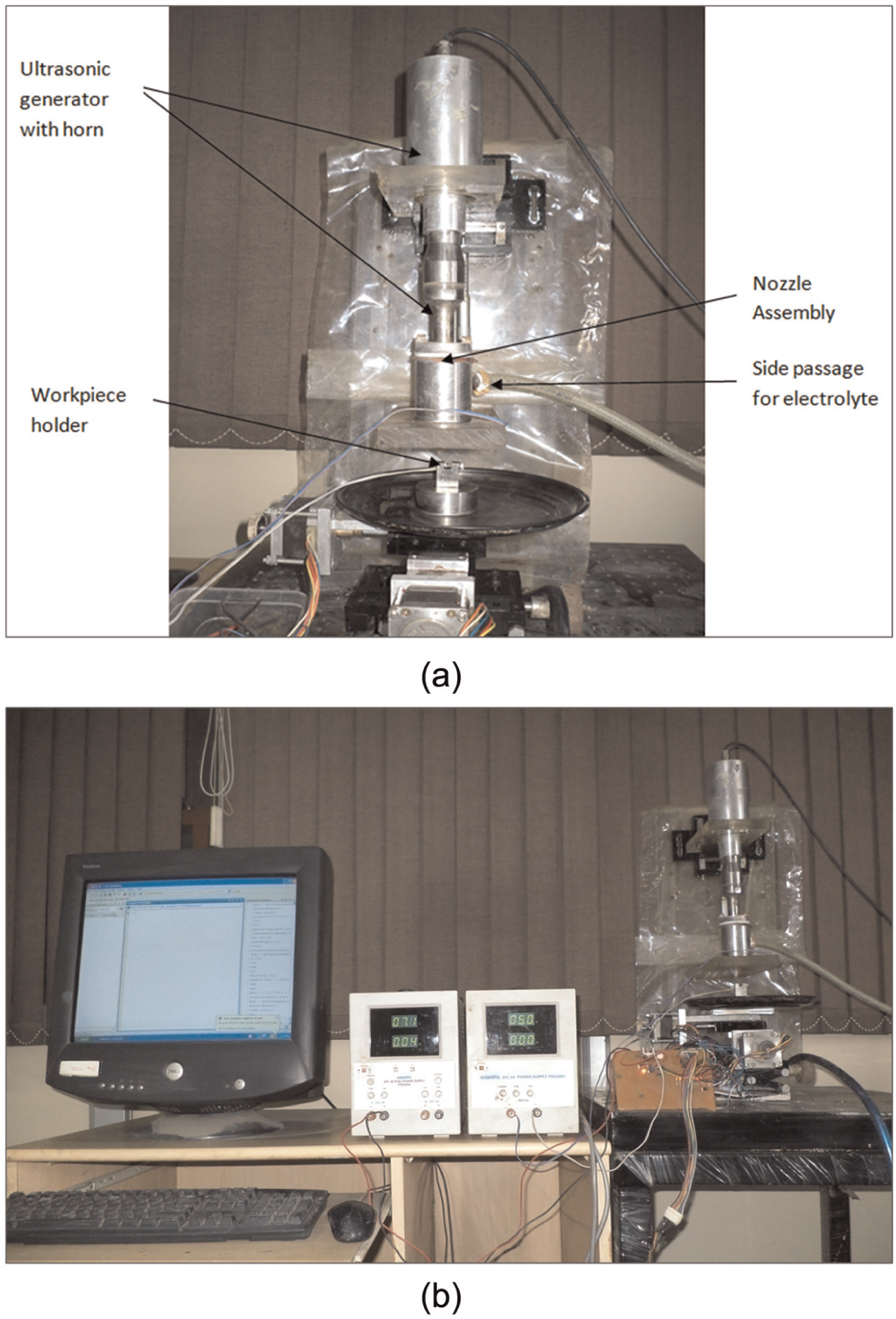
Picture of ultrasonic-assisted jet electrodeposition set-up: (a) nozzle assembly of UAJE set-up and (b) UAJE set-up.
Activation of nozzle and substrate as anode and cathode causes flow of current through the jet. Pulsed waveform power is supplied to anode and cathode. Ultrasonic vibrations (at 20 kHz) are given to electrolyte through horn of ultrasonic generator unit. These vibrations travel through electrolyte as longitudinal waves and reach to the substrate from jet. The amplitude of ultrasonic vibrations at the end of ultrasonic horn was registered at surface from which vibrations are transmitted to electrolyte, as shown in Figure 5, by a Fast Fourier Transform (FFT) analyser (Model-2200; Make-Diagnostic Instruments, US) at 720 W power of ultrasonic unit. The transducer of FFT analyser was attached to the vibrating surface, which measured the acceleration of the vibrating end, and was converted to amplitude of the vibrations as a function of time, as shown in Figure 5. Pressurized air is supplied to electrolyte tank by the compressor. The high pressure air is utilized to provide pressurized electrolyte to the nozzle. The high-pressure electrolyte is ejected through nozzle opening. The ejected electrolyte forms a jet when it comes out from opening.
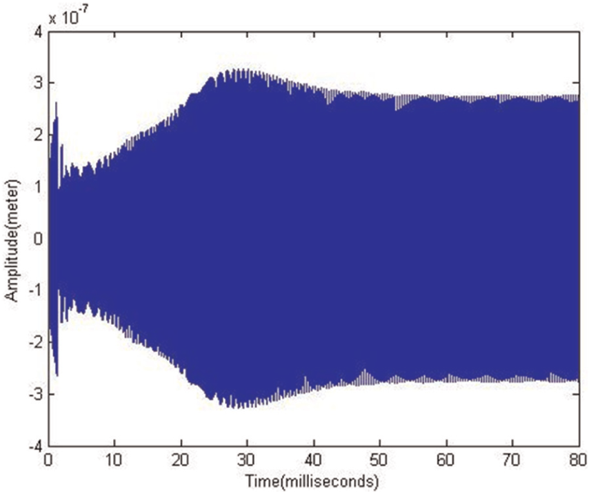
Ultrasonic vibrations (at 20 kHz) transmitted to electrolyte at nozzle assembly.
Experimentation
Pulse current deposition may control the size of the microstructure (grain size) of deposited metal or alloys more effectively by varying the pulse frequency (f), the pulse length, that is, current on time (ton), time between two pluses, that is, current off time (toff) and duty cycle (θ). 13 The frequency (f) and duty cycle (θ) in terms of pulse length, that is, current on time (ton), time between two pluses, that is, current off time (toff), are given in equations (1) and (2)


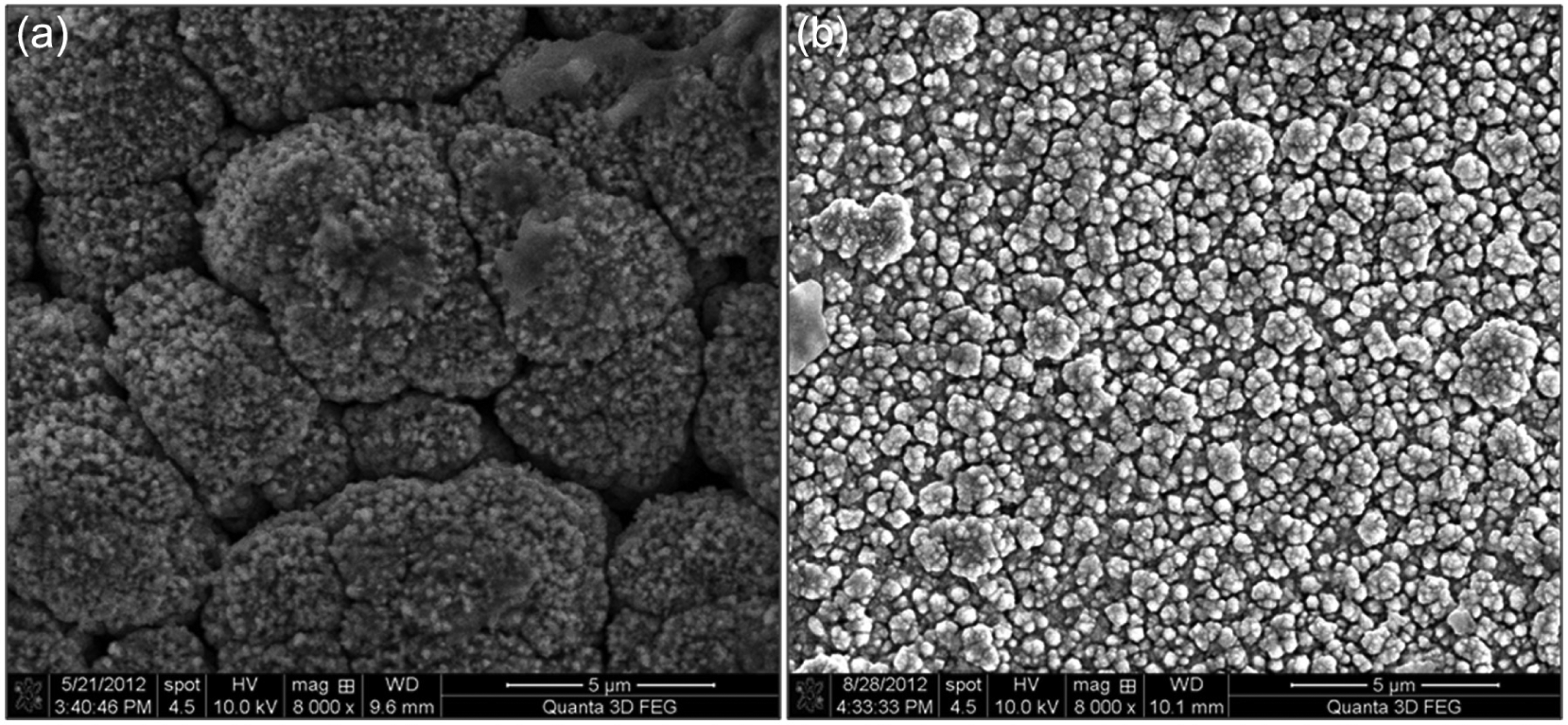
From equations (1) and (2), it is clear that by varying the frequency and duty cycle, current on time and current off time can be controlled. Therefore, frequency and duty cycle were selected as controllable process parameters for the experiments. The frequency was varied between 647 and 1354 Hz. The duty cycle was kept in between 10% and 22%. The parameters were selected on the basis of the literature 13 and pilot experiments so that it could produce nano-sized grains. Other parameters such as voltage, concentration of metallic ions, that is, CuSO4·5H2O, pulse on time of ultrasonic vibrations and gap between nozzle and substrate were kept constant (values are given in Table 2) for pulsed current UAJE experiments. A square profile micro part has been shown in Figure 6, 11 which is fabricated by continuous direct current UAJE. Similar features are fabricated to get the optimum values of the constant parameters (Table 2) for maximum accuracy and deposition rate. 11 The manufacturing time for the pulsed current UAJE process was kept constant for 120 min on the basis of pilot experiments. Micro parts were manufactured by moving the jet relatively to substrate surface in square shape of 500 µm side. The path is scanned for 120 times to achieve thickness of part. The scanned path has been shown in Figure 7(a). Figure 7(b)–(d) shows the SEM micrographs of fabricated features. The corresponding parameters of these fabricated features are given in Table 3.
Parameters kept constant during the experimentation.
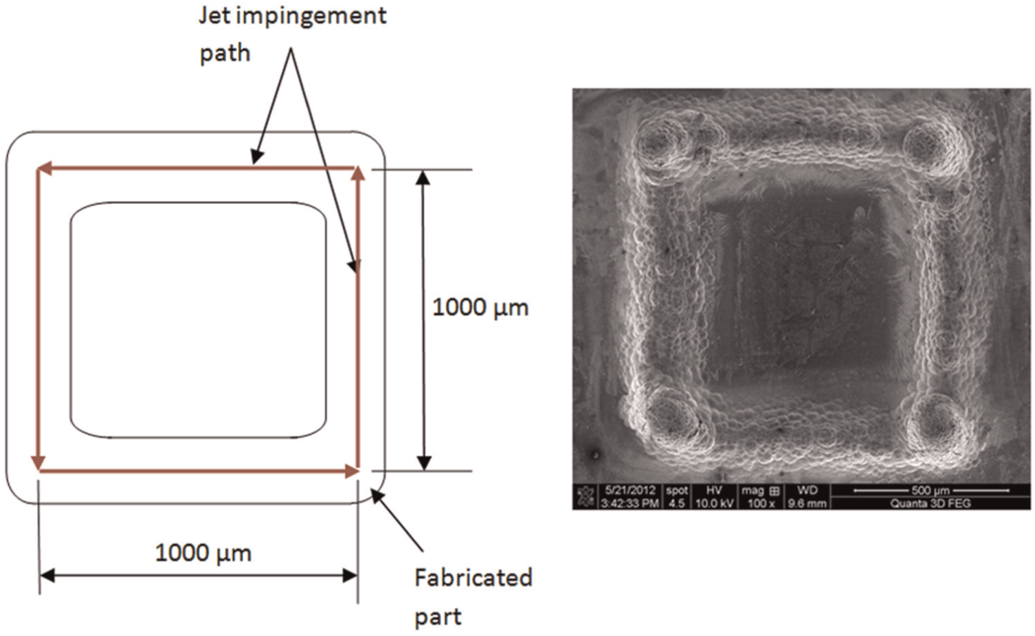
Micro feature built by direct current UAJE process at 7 V, 0.6 s, 19 g/L and 1.5 mm. 11
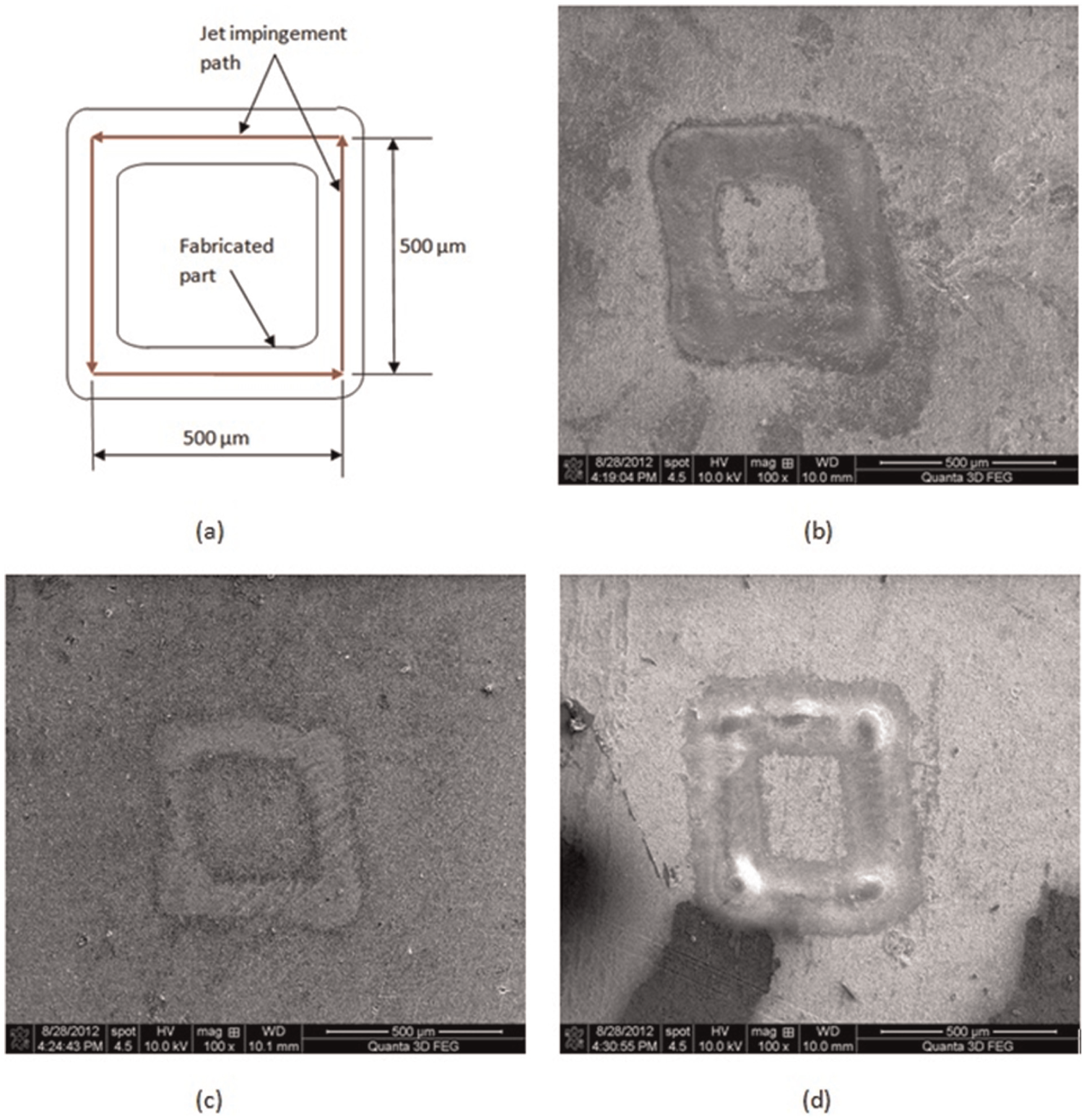
Micro features fabricated by pulsed current UAJE process and scanned path of jet over substrate: (a) path of jet relative to work surface and (b–d) fabricated features at different parametric conditions of pulsed current UAJE process.
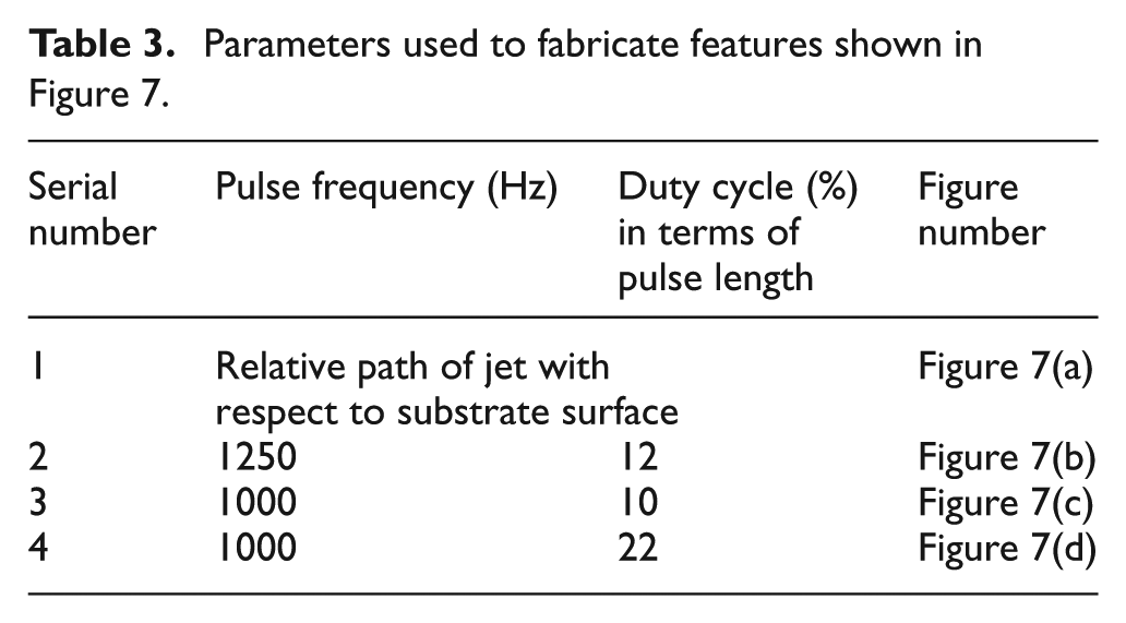
Parameters used to fabricate features shown in Figure 7.
Quanta 3D FEG machine has been used to capture the SEM images of fabricated features and their grain structure. The grains of micro features, which have been fabricated by pulsed current and direct current supply, are compared at 8000× magnification, and it is shown in Figure 8. The grains of features, which have been fabricated by pulsed current supply, are shown in Figure 9. The direct current UAJE resulted into micro-sized grains, whereas the pulsed current UAJE can be utilized to produce nano-sized grain micro features. The size (nano-sized grains) of the grain is found to be varying with frequency and duty cycle. AFM images are also used for characterization of the surface morphology of deposited feature, as shown in Figure 10. It has been found that the features created by pulsed current UAJE have better upper (layer) surface morphology than the direct current UAJE. Surface smoothness of the pulse supply deposits was found to be better than direct current supply deposits due to the higher instantaneous current density by pulse supply. 13 The force–displacement curves have been plotted for surface of fabricated micro parts using AFM technique for studying the nanomechanical properties. The AFM cantilevers were calibrated for their sensitivity against the sapphire sample. The obtained properties of fabricated samples were found to vary according to the grain size. The microhardness of the part was measured by depositing 1-mm-thick layer over substrate at different parametric conditions similar to those which are utilized for fabrication of micro parts. The deposited layer was then polished and microhardness was measured. It was found different for distinct grain sizes produced at different parametric conditions. The details of the nanomechanical testing and microhardness studies are given in the next section.
Grain structure of micro features fabricated at 8000× by (a) direct current UAJE process and (b) pulsed current UAJE process (at 750 Hz and 12%).
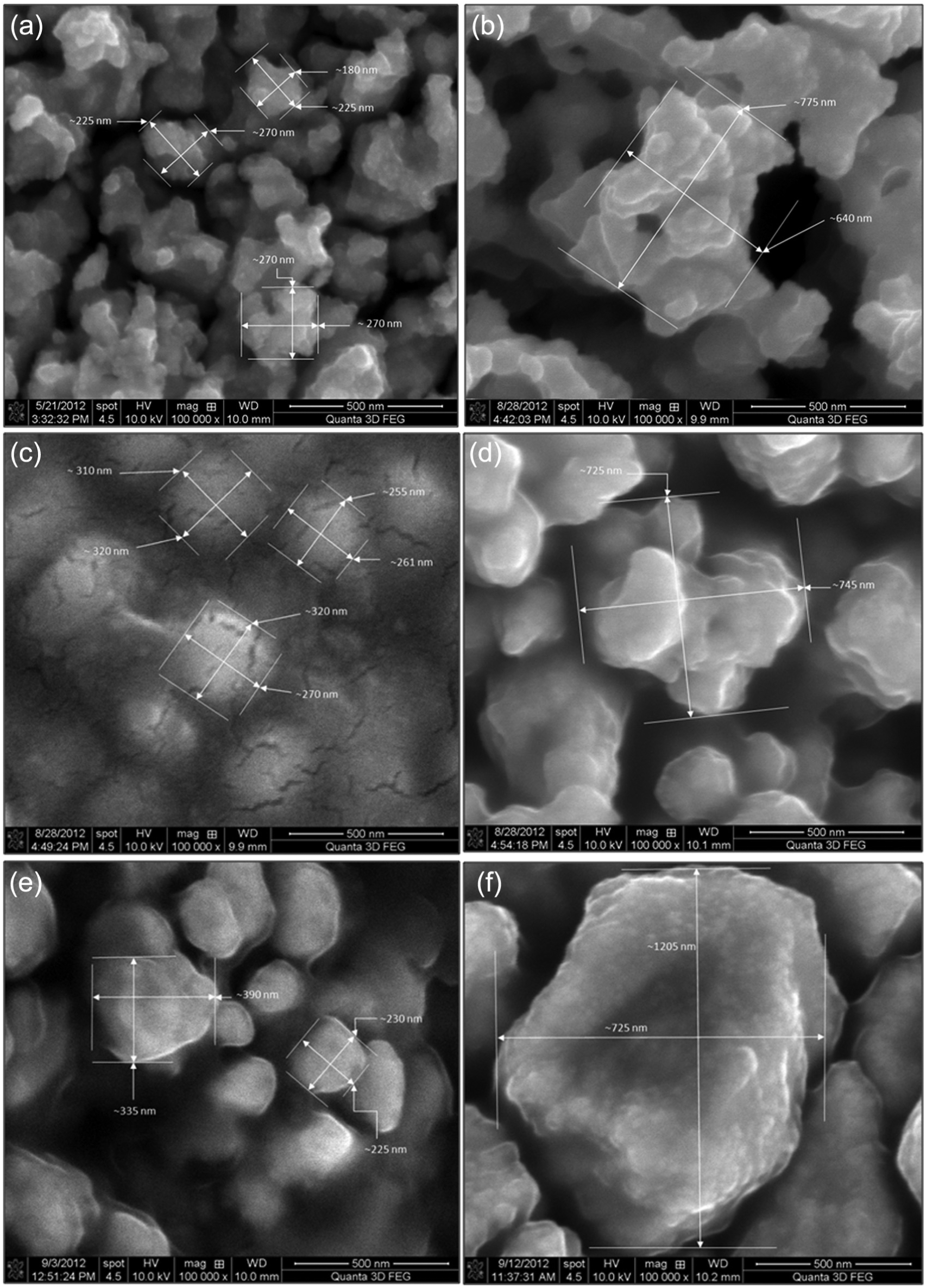
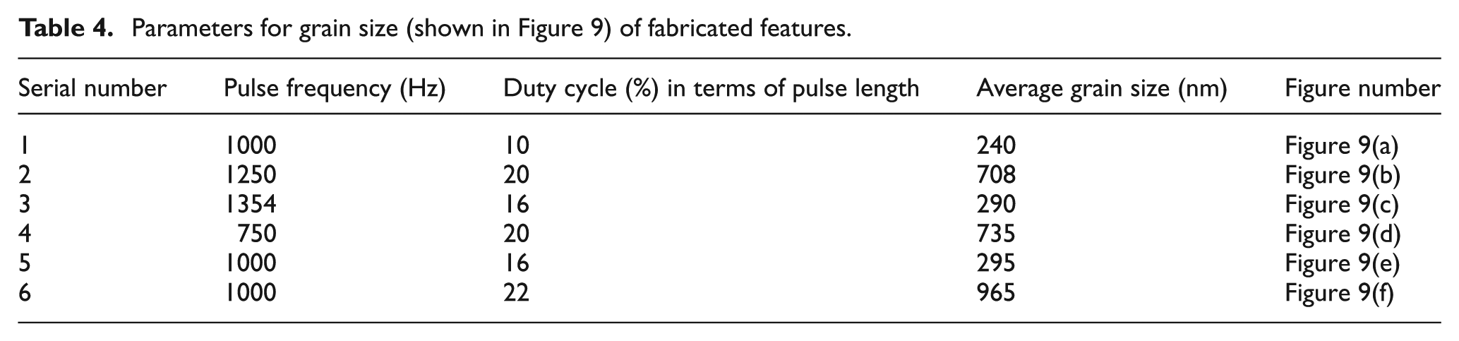
Grain structure of fabricated features at different parametric conditions at 100,000× (corresponding process parameters are presented in Table 4).
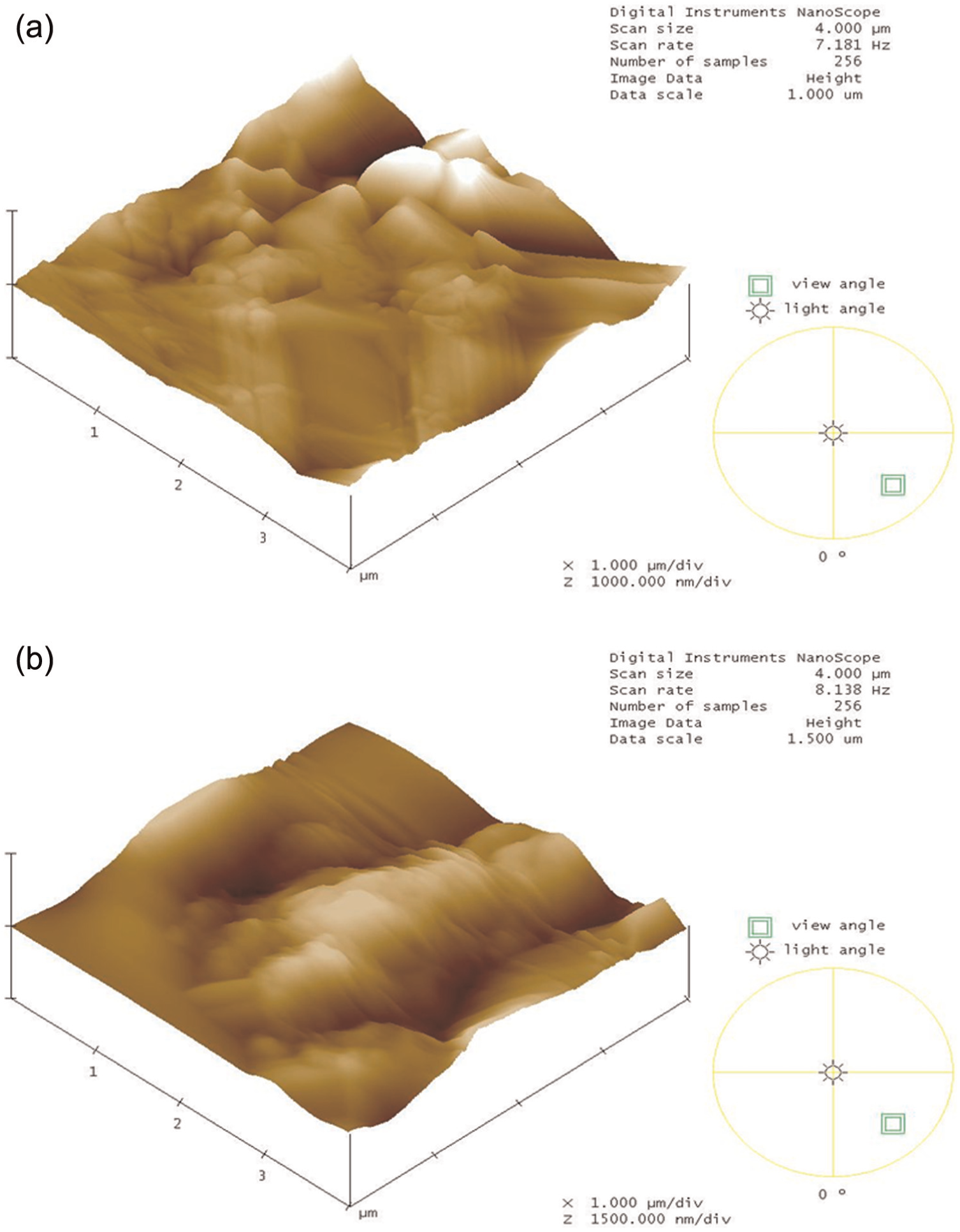
AFM images: (a) direct current UAJE depositions and (b) pulsed current UAJE depositions at frequency = 1356 Hz, duty cycle = 16%.
Results and discussion
Impact of process parameters on grain size
The SEM images of grain size obtained by the process are shown in Figure 9 and the corresponding parameters are presented in Table 4. The variation in grain size with process parameters is presented in Figure 11(a) and (b). The grain size is found to vary from 240 to 965 nm in pulsed current supply UAJE fabricated parts. The difference between grain sizes of micro parts fabricated by direct current and pulsed current supply UAJE process is depicted in Figure 8, and it has been found that the increase in frequency causes decrease in grain size. It is evident from equation (1) that the increase in frequency results in decreased current on time. The current flows between nozzle and workpiece result in chemical reduction of Cu++ ions (of electrolyte). Cu++ ions are deposited as copper 14 at substrate (workpiece).
Parameters for grain size (shown in Figure 9) of fabricated features.
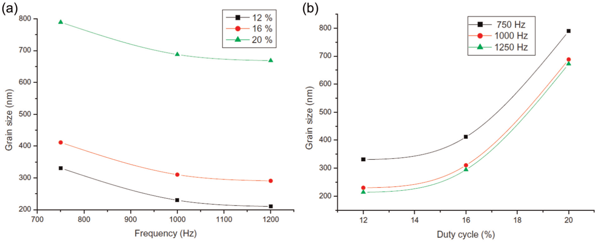
(a) Distribution of grain size with frequency and (b) variation in grain size with duty cycle.
The deposition of nano grains by pulsed electrodeposition depends on two fundamental processes: (1) the nucleation rate and (2) the growth of existing grains. 15 High nucleation rate and slow growth of existing grains are suitable conditions to cause fine grain deposits. The nucleation rate depends on the current density and pulse on time (ton). The current density was kept constant by keeping the voltage, gap and concentration fixed. The growth rate also depends on the current density and pulse on time (ton) as well as on the time between two pulses (toff). The important controllable parameters in pulsed current UAJE to produce nano-sized grain micro features are pulse on time (ton) and the time between two pulses (toff).
The pulse on time (ton) determines the number of ions that are deposited during a pulse, 15 which controls the size of grain. From equation (1), it is evident that the increase in frequency results in decreased current on time, that is, ton. This favours a condition of reduced number of ions to form nuclei and grain and results in fine grain deposits. Pulse off time (toff) is the time between two pulses. In this time period, the grain growth and nucleation on the substrate stop. This is the time gap, which stops deposition process and controls the repetition (formation of new nuclei) 15 of process. The deposition process again starts by the next coming pulse. This controls the nucleation rate. The ions are deposited as new nuclei rather than incorporated into existing crystals and then ultra-fine-grained deposits are obtained. 13
Duty cycle has been represented in percentage in this study. According to equation (2) on increasing the duty cycle, current on time (ton) of a pulse also increases. This favours for more ion deposition at cathode during single pulse, which results in increased size of grains, as shown in Figure 11(b).
The micro feature fabricated by pulsed current supply UAJE was found more even, regular and uniform than micro feature fabricated by direct current UAJE. The AFM images of top surface of features, fabricated by direct current supply UAJE and pulsed current supply UAJE, are shown in Figure 10(a) and (b). In pulsed current supply electrodeposition process, higher current density is obtained due to reduced thickness of diffusion layer. 16 Diffusion layer is positive ion depleted layer, formed over cathode due to reduction reaction of ions. Particles having same charge apply repelling force to each other and intensity of force increases with decrease in distance between them. 17 Small diffusion layer favours more uniform distribution due to the increased intensity of repelling force caused by high density of ions over the substrate surface. This allows the discharge sites and deposition to be more uniformly distributed 18 and results in better finish of fabricated micro feature.
Impact of process parameters on force–displacement curve
The force–displacement diagram of micro features, fabricated by pulsed current UAJE process at different parametric conditions, is shown in Figure 12(a)–(c). In this technique, the probe of AFM system is moved over the fabricated surface. When the tip of probe reaches sufficiently near to the surface, the tip suddenly attaches to work surface by bending towards the surface due to the cohesive forces acting between the tip and the surface. At this condition, the force acting on the cantilever is attractive that is represented as negative force on the graph. The tip probe is subsequently moved further towards the surface. At a point, the deflection becomes negative to 0. The tip of probe is pressed again towards the fabricated sample. As the tip is pressed deep into the deposited material, the probe’s cantilever flexes. The amount of cantilever flexion for a given amount of downward tip movement gives an indication of the material’s resistance. At this time, the deflection force is found positive. The resistance force has been measured by the cantilever’s deflection. The contact force is defined by equation (3)

where k is the spring constant of cantilever and ΔZ is the distance from where cantilever starts flexing, which represents cantilever motion during the pressing of tip. The cantilever is extended till the maximum set value of deflection is achieved. The tip is pulled back and the corresponding force is measured. The cantilever again bends due to the holding up of the tip by the surface attraction (cohesive forces) in the opposite direction. It is also represented as negative force on the graph. As tip cantilever further bends, tip finally breaks free of surface attraction. After this, no further contact is obtained between the tip and the surface. The complete force–displacement behaviour has been shown pictorially in Figure 12. It is found that the generated surface, which has smaller grain size, produced greater amount of resistive force against probe tip motion as the grain size is a major parameter affecting grain boundary hardening. 13 Smaller gain size parts have better resistance towards indentation at nano level. It shows that hardness at nano level increases and elasticity reduces with decrease in grain size. This is found to be in compliance with Hall–Petch relationship, that is, nanocrystalline materials are expected to exhibit higher strength than their microcrystalline counterpart. 13 Nanocrystalline materials have more grain boundaries than the microcrystalline materials. These grain boundaries make nanocrystalline materials of higher strength due to restriction of motion of crystal defects and dislocations and results in higher hardness and lessened softness of deposited micro features.
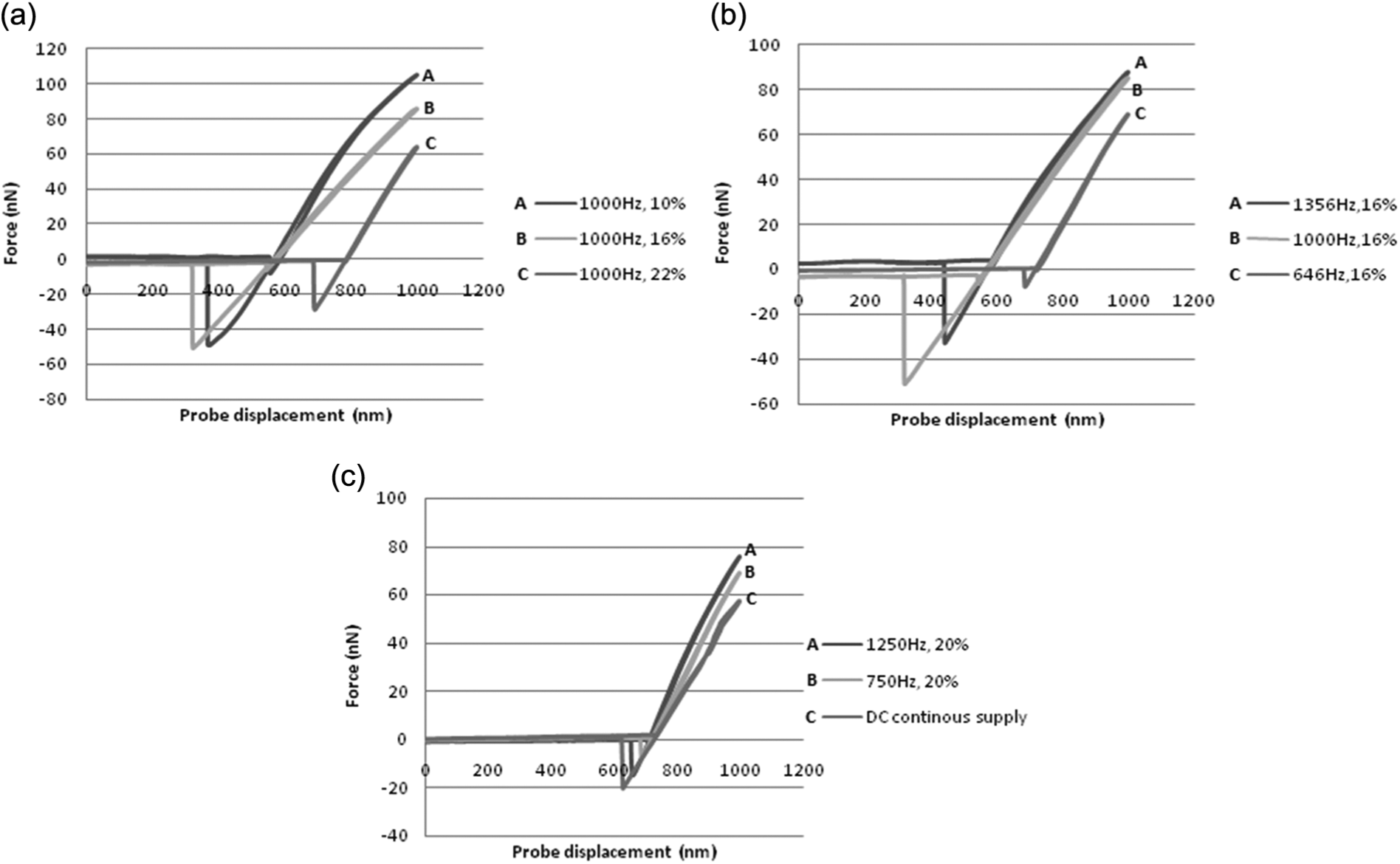
Force–displacement curves of fabricated surfaces at different parametric conditions.
Impact of process parameters on microhardness
Microhardness of fabricated samples has been measured, which are of different grain sizes. The variation in microhardness is shown in Figure 13. It has been found that the parts having smaller grain size have higher microhardness in comparison to the comparatively large grain parts (micro size grain). A nano-sized grain micro feature has higher microhardness than a micro-sized grain micro feature. 13 The key mechanism for grain refinement strengthening is that the dislocations are blocked by grain boundaries, and thus, it enhances the resistance to plastic deformation. 13
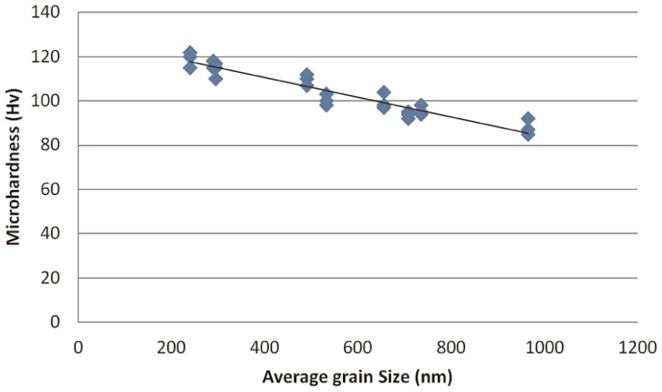
Microhardness variation with grain size.
Conclusion
Nano-sized grain and micro-sized grain features have been successfully fabricated using pulsed current UAJE and direct current UAJE processes, respectively. The fabricated parts have grain size in the range of 240–4000 nm. The desired grain size can be achieved by properly controlling frequency and duty cycle of pulsed current UAJE process. This enables to control the mechanical properties of fabricated parts. It has been found that nano-sized grain micro parts have greater resistance to indentation as compared to micro-sized grain micro parts at nano level. Thus, nanocrystalline micro features have superior nanomechanical properties. These properties are important for the potential application of micro features in devices such as microelectromechanical systems (MEMS), micro gear systems, orthogonal reflection optics systems and other micromechanical systems. The microhardness of fabricated parts also varied according to grain size, and it has been found varying from 122 to 80 Hv as per the grain size. Mechanical properties of the nano-sized grain (pulsed current UAJE fabricated) micro feature are markedly superior to those of the micro-sized grain (direct current UAJE) micro feature.
Footnotes
Acknowledgements
The authors gratefully acknowledge the support provided by council of scientific and industrial research (CSIR), New Delhi, India, for carrying out this study.
Declaration of conflicting interests
The authors declare that there is no conflict of interest.
Funding
The financial assistance to carry out this study was obtained from the Indian Institute of Technology Delhi.