
Abstract
Poor chip breakage causes problems in machining of low-lead brass. To improve chip breakage, finite element model simulations were implemented in cutting tool design. Finite element model simulations enable high number of experiments that would be expensive and slow to perform by conventional cutting tests. Compression tests and cutting experiments under different temperatures and strain rates were performed for lead-free brass, to acquire material parameters for the finite element model. It was observed that the coupled effect of thermal softening and rate sensitivity of the material was difficult to take into account with the existing material model. Furthermore, it was found that there are no reported material models that can take rate sensitivity–temperature coupling into account. This was counteracted by fitting the model with least square method to the stress–strain data at the cutting temperature, although this causes error in simulations with temperatures higher or lower than the supposed cutting temperature. Nevertheless, the simulated results proved accurate enough to model the chip breakage. Based on the simulations and experiments, the use of a positive rake angle, high cutting speed and low cutting feed rate improve chip breakage from continuous chip to a chip of average length of 4 mm.
Introduction
Health and environmental issues are growing concerns for companies and governmental decisions. In the United States, the state of California has banned plumbing products containing lead more than 0.25%. 1 The restriction took effect on 1 January 2010 despite the opposition of The Plumbing Manufacturers Institute. 2 Exposure to lead is a commonly known major health hazard, as it can cause anaemia and provoke other health issues. 3 The restriction affects especially brass components, which are typically machined from cast billets. Typical cast brass alloys with good machinability contain lead between 1.5% and 3%. 4 Some companies have decided to substitute lead with bismuth, although there are references according to which bismuth could also be toxic.5,6 Finnish faucet and plumbing industry has decided to use lead-free brass (<0.25 Pb%) in their production. The decision has caused difficulties in machining, especially because poor chip breakage of lead-free casting brass causes jamming of the machine tool and bad-quality products because the chips are tearing the final product. This article studies chip breakage of lead-free brass in machining operations with the help of finite element simulations and extensive material characterization. The goal of this study is to develop a method for cutting lead-free brass products without generating continuous chip.
In previous research by Laakso, 7 finite element modelling of cutting was evaluated by comparing simulated results to experimental data acquired for stainless steel, carbon steel and aluminium in different machining processes. Simulation software used in the study were Third Wave Systems AdvantEdge and Parametric Forming Technologies Deform. Although it was concluded that simulations generally give fair approximation (<30% error in cutting forces), the qualitative behaviour of cutting simulations is in line with experimental results. Therefore, it is reasonable to assume that simulations can predict the effect of different cutting parameters to chip breakage accurately enough. From the study, it was concluded that the material model has the most significant impact on accuracy apart from the geometrical accuracy of the tool and the friction model. Other studies report similar results. Yen et al. studied the effect of tool geometry on cutting forces and temperature. Good correlation between experimental and simulated forces was found with different cutting edge radiuses. The error in the forces was between 5% and 13%. The cutting force increases as the radius increases. Temperature was concluded to be directly proportional to amount of plastic deformation, which is directly proportional to tool edge radius. Therefore, temperature is proportional to cutting force. 8 Mackerle9,10 has listed research articles about finite element simulations of metal cutting from 1976 to 2002 in his bibliography review. Childs included upper yield stress to power law material model. It was concluded that for steels, the effect of upper yield stress is significant, and the standard error in cutting, which is underestimated cutting force in simulations, was not found when using the improved model.11,12 This implicates that other material phenomenon such as temperature and rate sensitivity coupling considered to be negligible in metal cutting could prove to be significant factor in simulation accuracy. Coupled effect of rate sensitivity and temperature was reported in the studies by Suery and Baudelet 13 and Jiang et al., 14 but it was not emphasized how important the effect is on machining. Also, as discussed in the study by Childs, 15 the friction in cutting process does not follow the Coulomb friction law. Few attempts to correct this have been reported.16–18
Materials and methods
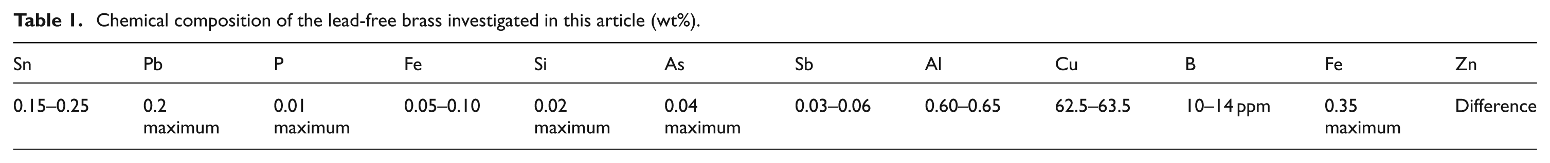
The AdvantEdge 19 cutting simulation software was used for the simulations. The software was first presented in the study by Marusich and Ortiz. 20 The software is based on a dynamic explicit Lagrangian finite element model (FEM), which employs adaptive remeshing to avoid element distortions. The model is based on equations of motion and thermo-mechanically coupled material model.20,21 The casting brass investigated in this article is not standardized, but is close to standard EN CW511L. The composition of the brass is presented inTable 1. A material model based on the power law equation was implemented to mathematically reproduce the constitutive behaviour of the material. The model is built-in in the AdvantEdge FEM software. To implement the model, material behaviour and parameters were determined from a series of compression tests and cutting experiments performed at different strain rates and temperatures.
Chemical composition of the lead-free brass investigated in this article (wt%).
Material model
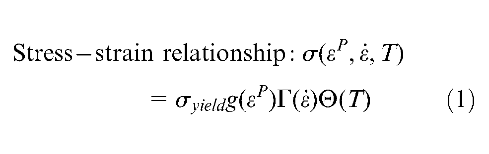
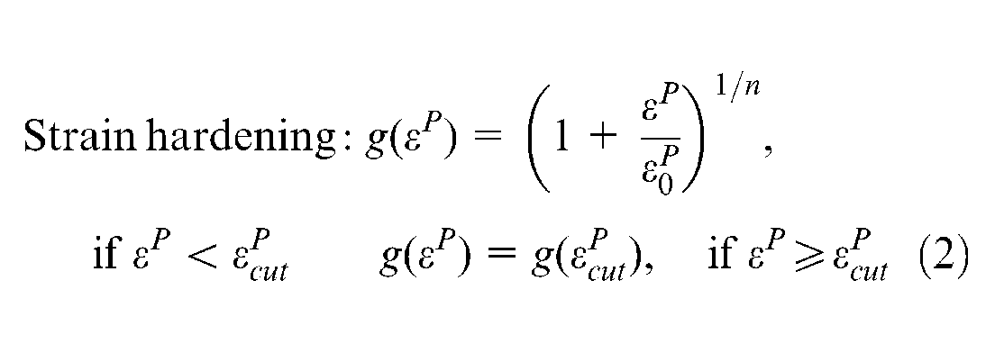
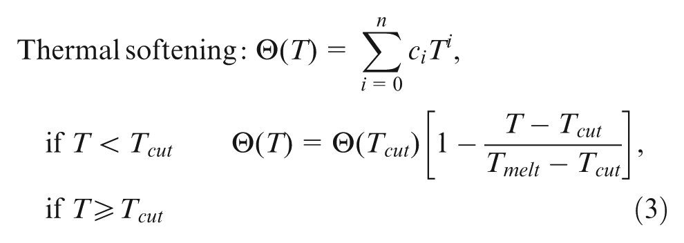
A mathematical formulation of the flow stress model is presented in equations (1)–(4) (AdvantEdge User Manual, 20). This model takes into account strain hardening, thermal softening and strain rate hardening. The stress–strain relationship is composed of three parts: strain hardening multiplier,
2
thermal softening multiplier
3
and strain rate hardening multiplier.
4
Each of these multipliers takes the corresponding input parameter. Multipliers adjust the value of yield stress (flow stress) to the measured stress–strain curve in different conditions. The input parameters are strain ε, temperature T and strain rate
Material testing
Material testing was conducted by a series of compression tests at different temperatures and strain rates from 10−3 to 3200 s−1. The range of strain rates used is limited by the capabilities of the testing platform available. Testing temperatures are selected to room temperature, expected cutting temperature and the highest temperature achievable by the testing oven. A few tensile tests were also conducted to observe if any significant differences between tension and compression exist. The low-strain rate tests (≤10−1 s−1) were conducted using a servo hydraulic material testing machine with an induction heating system. The high-strain rate tests were done using a Split Hopkinson Pressure Bar device equipped with a special high-temperature set-up. These compression tests were done at strain rates ranging from 1000 up to 3200 s−1 at room temperature and at elevated temperatures of 200 °C and 450 °C. For example, the devices used in this work are described in more detail in the studies by Apostol et al.23–25
Simulations
The simulations were carried out by the AdvantEdge software running on a server-based PC with twenty-four 3.6-GHz Intel Xeon Cores, 32 GB of memory, Nvidia Quadro FX 1800 graphics card and 3500 GB hard drives on RAID 5 configuration to enhance read/write performance. A 2D mode turning operation was employed for the simulations, which were conducted with three different cutting speeds (50, 150 and 300 m/min), three different feed rates (0.1, 0.2 and 0.4 mm/r) and rake angles of +5° and −5°. Cutting tool angle of 90° was used due to orthogonal condition of the 2D simulations. Cutting forces, temperatures and chip thicknesses were recorded as output. Chip breakage was evaluated by the number of near breaking points and chip breakage at chip root as presented in Figure 8 of Balaji et al.’s 26 study.
Cutting experiments
Strain rates above 104 s−1 are very difficult to achieve using the Hopkinson Bar techniques, and therefore, cutting experiments were conducted to obtain stress–strain data at these strain rates. A manual lathe and force measuring equipment, KISTLER 9257A piezoelectric sensor and 5019A charge amplifier, were used in the experiments. The forces to the direction of primary cutting motion, Fc, and to the direction of feed, Ff, are measured. Due to the lack of valid analytical models for cutting, an inverse analysis between force measurements and FEM analysis was conducted to acquire the stress–strain relationship. Inverse routine starts by fitting the material flow stress model presented in equations (1)–(4) to compression test data, then using the model to simulate some specific cutting experiment and improving the model by comparing the simulated results to experimental results. Usually, cutting force is used in evaluation, but also chip thickness is used in some cases. The model is then adjusted to produce better values. The parameters to adjust are εcut,
Results
First, the results of the compression tests and cutting experiments are given. Then, the material model fitting and analysis of it are presented. The simulated results are presented after the modelling details, because they are prerequisites for simulations. The last part compares the results obtained from the simulations and experiments.
Compression tests
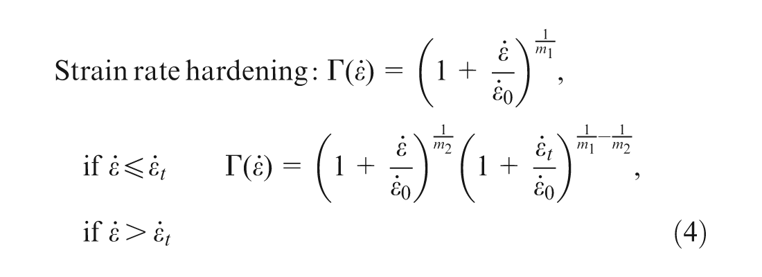
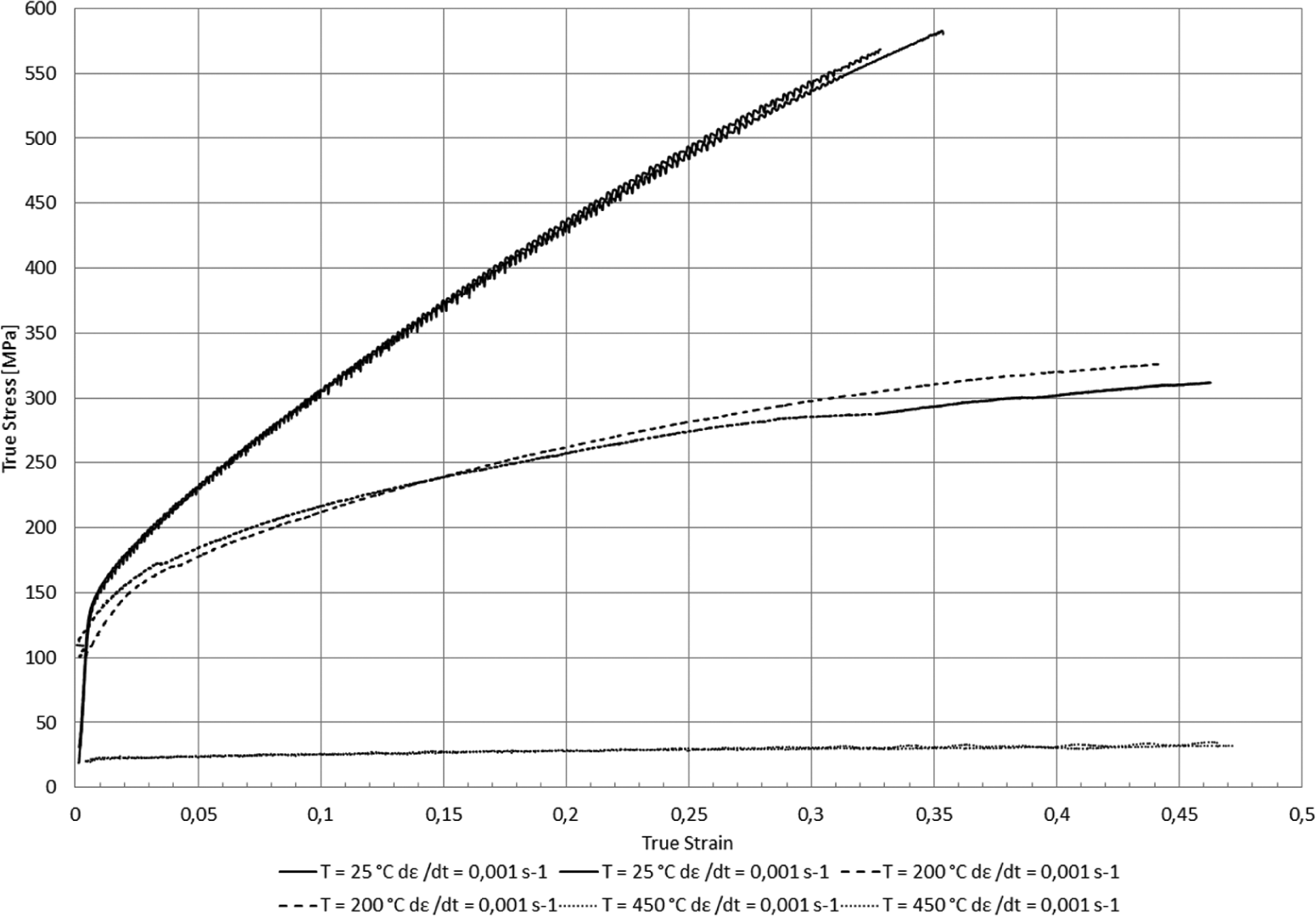
Figure 1 shows the results of the compression tests done at strain rates of 10−3 s−1. The yield strength of the material at room temperature is around 145 MPa. Yield strength does not depend much on strain rate, which can be seen by comparing Figure 1 with Figure 2. This is a typical behaviour of a simple face-centred cubic (FCC) metal. Also, strain hardening rate seen as the slope of the curve is fairly strong and nearly constant with respect to strain, up to fairly large strains. When the temperature is increased to 200 °C, the yield strength of the material does not change much, but the strain hardening rate decreases significantly. Also, the strain rate sensitivity of the material increases especially at larger strains, which is an indication of increasing amount of thermally activated dislocation glide obstacles. 27 For a FCC metal, the most significant thermally activated event is the cutting of forest dislocations, the number of which increases with strain. Even at higher temperature, not only the strain hardening rate drops further but also the yield strength decreases significantly. This might be an indication of recrystallization and/or grain growth at this temperature.
Compression stress–strain curves obtained at different temperatures and at the strain rate of 10−3 s−1.
Compression stress–strain curves obtained at different temperatures and at the strain rate of 10−1 s−1.
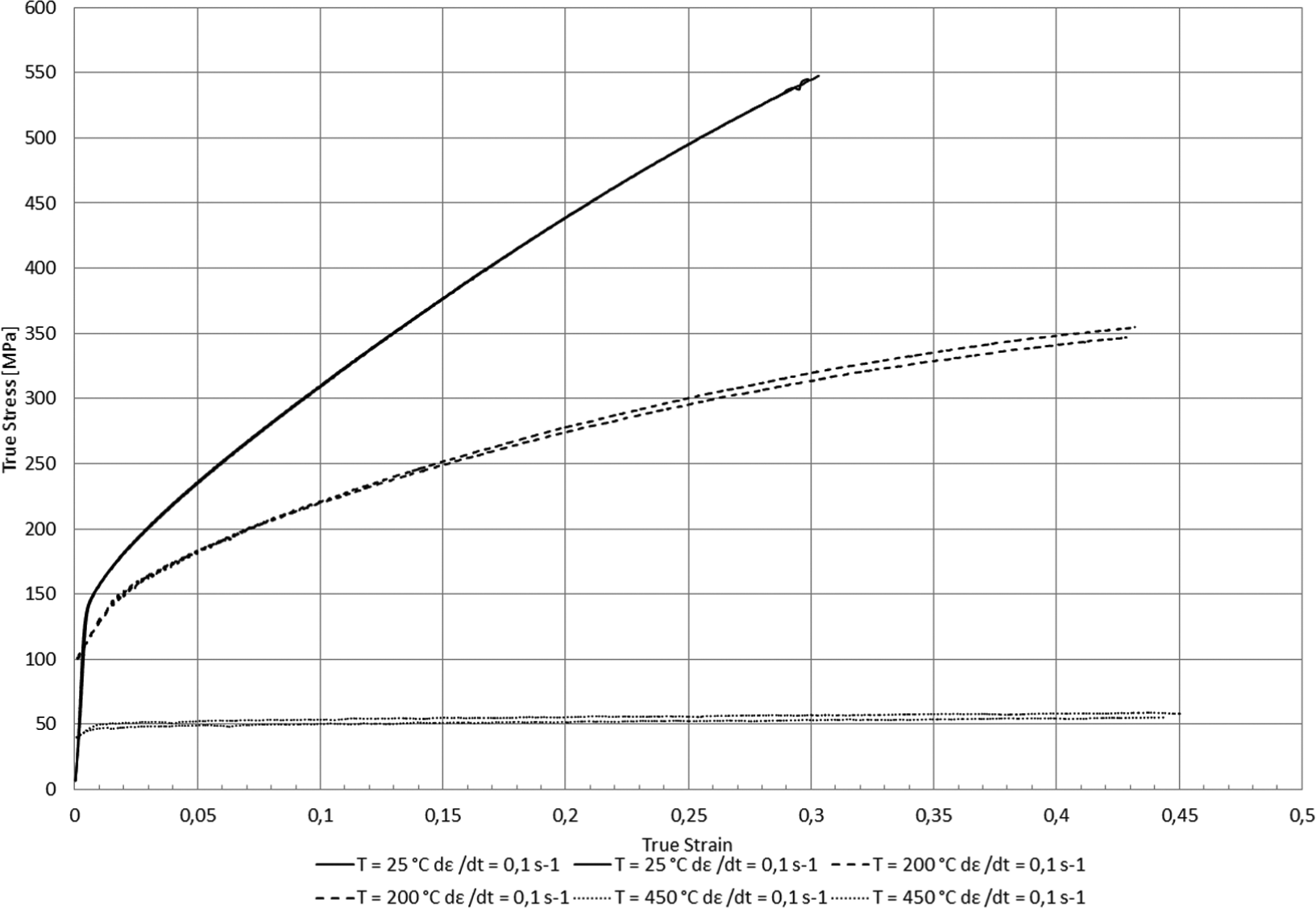
Figures 3 and 4 present the results of the compression tests done at high strain rates. The yield strength of the material seems to be fairly insensitive to strain rate, and only a modest increase to about 170 MPa is observed at the highest strain rates. The strain hardening rate, however, increases strongly compared to the low-strain rate tests. At high strain rates, the temperature seems to have much less effect on the strength and strain hardening behaviour of the material when compared to that observed at low strain rates. The yield strength of the material decreases only from 170 to about 145 MPa at 450 °C and at 1300 s−1, and also the strain hardening rate is only slightly decreased at higher temperatures. This is an important result, because material models generally do not take this behaviour into account.
Compression stress–strain curves obtained at different temperatures at the strain rate of ~1300 s−1.
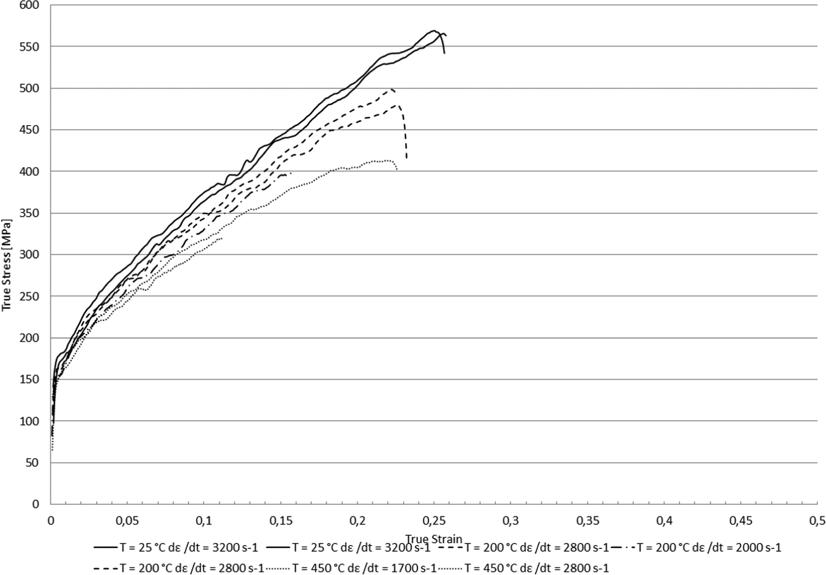
Compression stress–strain curves obtained at different temperatures at the strain rates of 1700–3200 s−1.
Similar rate sensitivity and temperature behaviour were observed for 60/40 brass in research conducted by Suery and Baudelet. Yield stress at 600 °C increased from 50 to over 200 MPa when strain rate increased from 10−2 to 0.4 s−1. 15 Jiang et al. conducted experiments on 7050-T7451 aluminium to simulate turning with power law material model. Similar procedure as in this article was done to acquire material parameters. Split Hopkinson tests revealed that yield stress of aluminium at 300 °C increases from 350 to 500 MPa when strain rate increases from 10−3 to 6200 s−1. The increase of yield stress with increasing strain rate is not significant at room temperature. 16
Cutting experiments
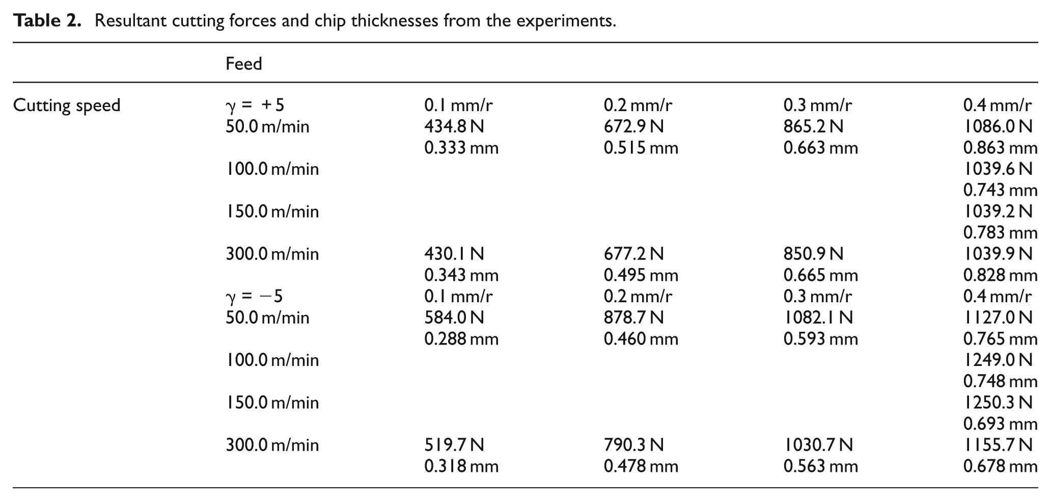
Results of the cutting experiments are presented in Table 2. The forces are presented as the resultant of the cutting force acting in the direction of primary cutting motion and the tangential force acting in the direction of feed. The resultant cutting forces increase almost linearly with the increase of cutting feed rate. Cutting speed does not have a significant impact, except a minor decrease of cutting forces at the highest speeds with a negative rake angle. Similar results were also observed with chip thicknesses. Cutting forces are clearly higher in the negative rake angle experiments. Chip breakage was observed by visual appearance and the length and thickness of the chip. The best results in chip breakage were observed at low feed rates. High cutting speed was also observed to improve surface roughness, although this was not measured as it was not in the scope of the research.
Resultant cutting forces and chip thicknesses from the experiments.
Material parameters
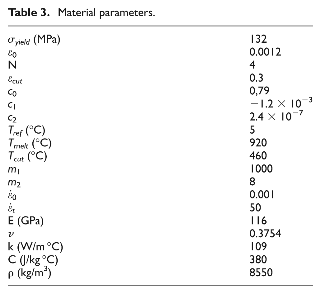
Material parameter values in Table 3 were determined to fit the model (equations (1)–(4)) to the stress–strain data obtained from the compression tests. Material parameters were fitted by the method of least squares. Other parameters needed by the simulation software are elastic modulus, Poisson’s ratio, thermal conductivity, heat capacity and density. All these values are found in engineering reference books or databases. Figures 5 and 6 present the multipliers for strain rate hardening and thermal softening. After the compression tests, εcut was set to 0.2. Simulated results while using this value showed greatly underestimated values for the resultant cutting forces so the value was increased to 0.3. After that, the forces were in much better agreement. Jiang et al. discussed the determining of strain cut-off value from orthogonal turning experiments by comparing simulated and experimental chip thicknesses and cutting forces. They concluded that strain cut-off value has major impact on simulated cutting forces and chip thickness. 16 The strain rate coefficients were chosen on the basis of the compression test results: the high-strain rate hardening zone seems to be as low as 50 s−1; therefore, the compression tests at the range used were adequate to model the strain rate hardening. Thermal softening was the most difficult to model because there are two distinctly different softening curves depending on the strain rate. The observed reduced thermal softening at high strain rates caused some difficulties in modelling the behaviour, as the model does not take such behaviour into account. The softening parameters were chosen as medium of the two different softening curves. Therefore, the model was fitted to the results obtained at 200 °C, which is the expected cutting temperature. This can be seen in Figures 5 and 6 as deviation of the model from the data points in temperatures lower or higher than 200 °C. The thermal softening effect is extreme after the material reaches cut-off value of 460 °C, after which the material flow stress goes linearly towards 0 and reaches it at the melting temperature.
Material parameters.
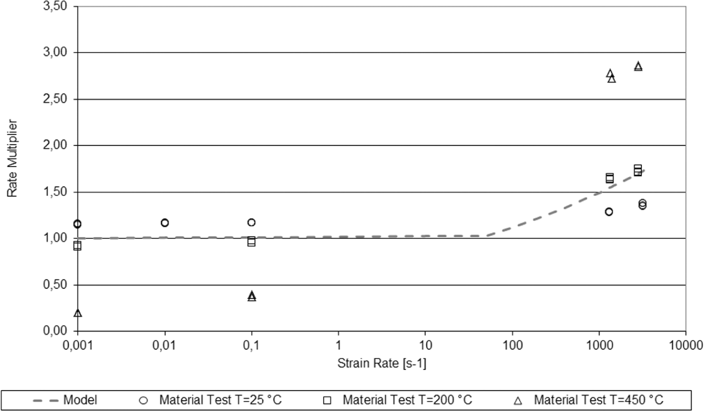
Rate multiplier fit by the method of least squares; the high deviation is caused by the material constitutive model, not by fitting method; the model is fitted to data in 200 °C.
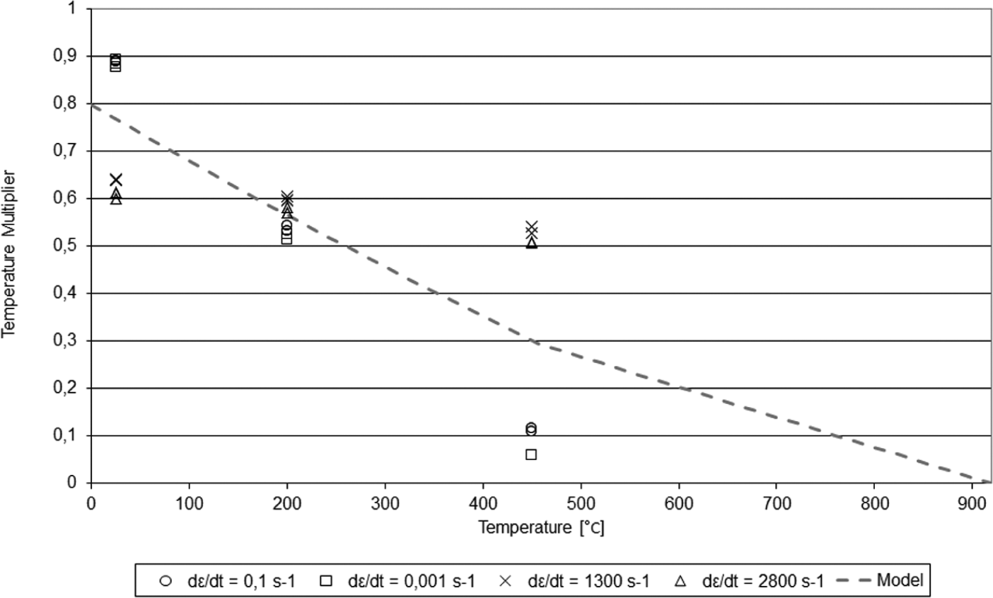
Temperature multiplier fit by the method of least squares; the high deviation is caused by the material constitutive model, not by fitting method; material flow stress reduces to 0 at the melting temperature of 920 °C as defined by the material model.
Simulations
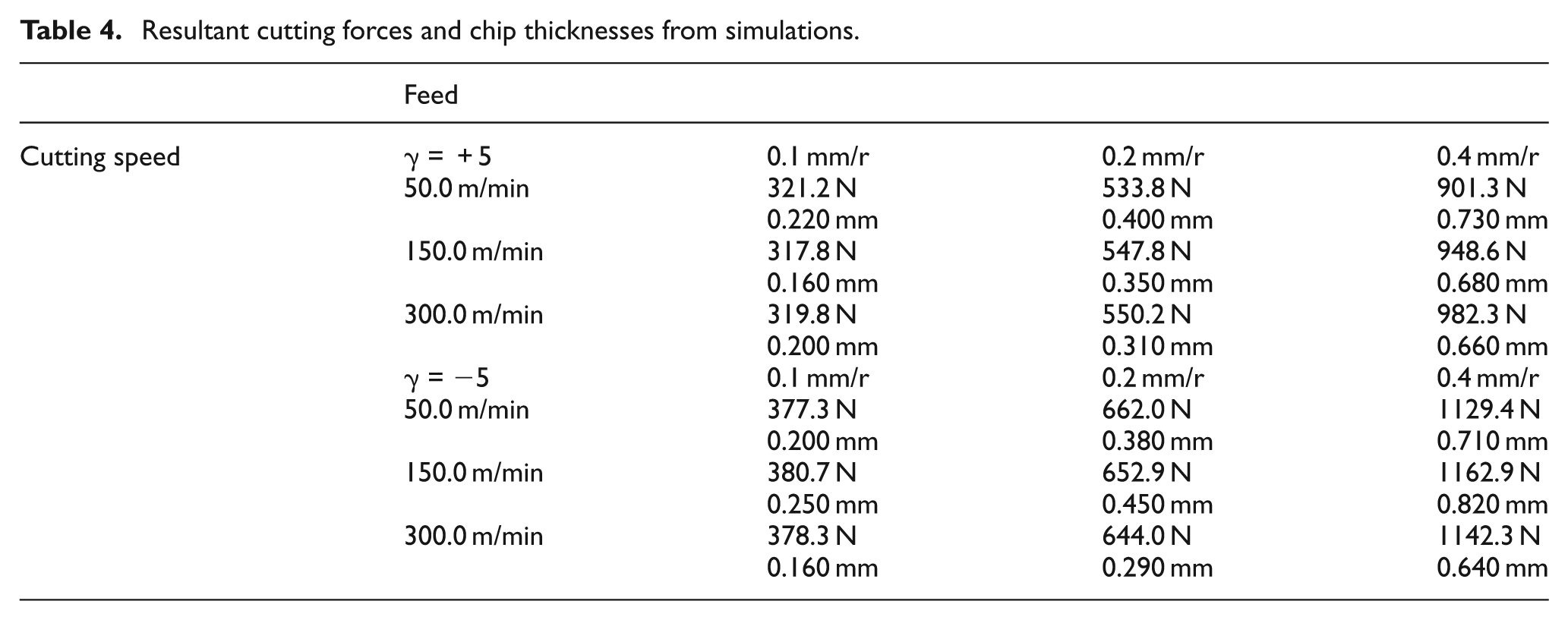
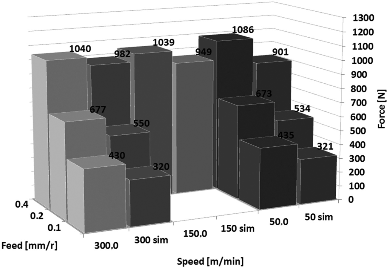
The simulated resultant cutting forces and chip thicknesses are presented in Table 4. Machinability is generally measured not only by chip thickness ratio but also by chip compression ratio. In this article, the chip thickness is used as measure for simulation error, not as criterion of machinability. The resultant cutting forces and chip thicknesses increase with increasing feed rate, but cutting speed does not have a major influence. The results show higher forces with negative rake angles. This is not unusual behaviour as it has been presented in many textbooks of the field. The higher forces are caused by the larger amount of plastic deformation in the chip formation zone.28–30 Chip breakage was best at high feed rates and speeds as explained in Appendix 1. The highest number of breaking and near breaking points was observed at 300 m/min with feed rate of 0.1 mm/r and +5° rake angle where 1 breaking and 1 near breaking points were observed at cutting length of 10 mm. The second best breakage was observed with same cutting parameters but with −5° rake angle; there were two near breaking points. Only three other cutting conditions lead to any breakage at all in 10 mm length of cut; these were at 150 m/min and 0.1 mm/r feed rate with +5° rake angle and at 300 m/min and 0.2 mm/r with both positive and negative rake angles. All of the simulation images are found in Appendix 1. Visualization of the chip breakage in Figure 7 is done by giving a score of 0.5 for one near breaking point and 1 for breaking point and summing it up as a score for each cutting condition.
Resultant cutting forces and chip thicknesses from simulations.
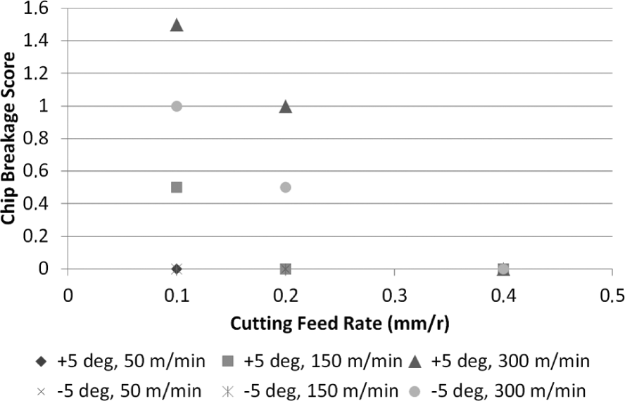
Chip breakage comparison, higher the score the better chip breakage.
Comparison
Figures 8 and 9 present the simulated and tested resultant cutting forces. It can be seen that the forces are in best agreement at high feed rate values. The higher difference at low feed rates can be explained by the lack of accuracy of the friction model. 17 Friction models tend to underestimate friction force in cutting. Friction force is a component in each of the three primary cutting force and therefore also a part of resultant force. Therefore, in higher feed rates, the force induced by friction between tool and chip is small in relation to the primary cutting force caused by the energy consumed in plastic deformation. That is the friction model tends to underestimate the resultant force in small values of feed rate, so the error is not as significant in the resultant cutting force in high feed rates as it is in lower feed rates. Also, as the simulations are 2D, the lack of a third force component tends to underestimate the resultant force. The error is in an acceptable range (average of <17%), compared to traditional analytical models (errors of >50% are not unusual). Qualitative behaviour of the simulations is more important than the exact values of the cutting force. A similar behaviour was perceived on chip thicknesses; the measured and simulated thicknesses were in best agreement with high feed rates (Figures 10 and 11). The best chip breakage was observed at low feed rates. Chip lengths at different cutting speeds and feed rates are presented in Figure 12. High cutting speed has also a minor positive impact on chip breakage. Although a better agreement in forces could have been achieved by adjusting model parameters, by changing the yield stress value higher or increasing the strain hardening exponent, the physical validity of the simulations would not have been correct. Therefore, qualitative behaviour would not have been correct either. Also, it should be mentioned that currently, there are no material models reported, which can take into account the coupled effect of rate sensitivity and temperature. Therefore, a new material model should be built around the test data, to improve the simulations and to observe the model’s impact on accuracy. Also, as many researchers have already suggested, a method to acquire the material parameters directly from cutting experiments should be developed. 31 Friction model should also be improved to reach better agreement with forces as the Coulomb friction is not valid in cutting because it has been shown that there is sliding between the chip and the tool. 32
Comparison of simulated and tested resultant cutting forces for a positive rake angle; experimental forces are averages of two experiments.
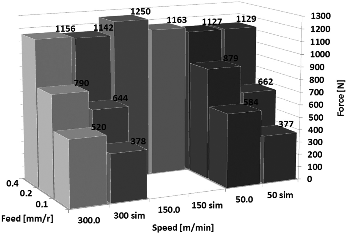
Comparison of simulated and tested resultant cutting forces for a negative rake angle; experimental forces are averages of two experiments.
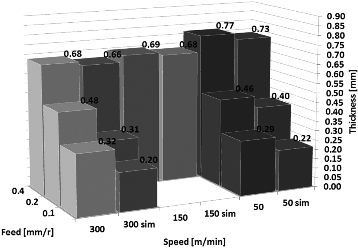
Comparison of simulated and measured chip thicknesses for a positive rake angle; experimental thicknesses are averages of five different chips.
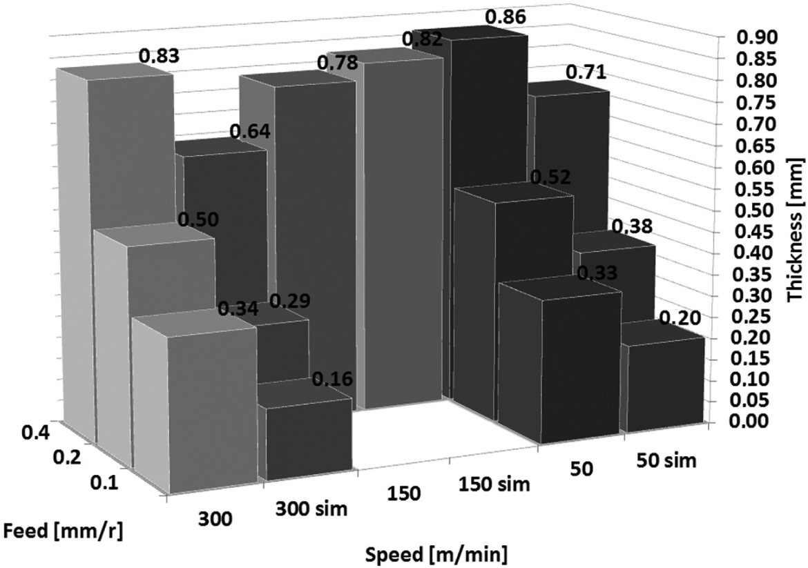
Comparison of simulated and measured chip thicknesses for a negative rake angle; experimental thicknesses are averages of five different chips.
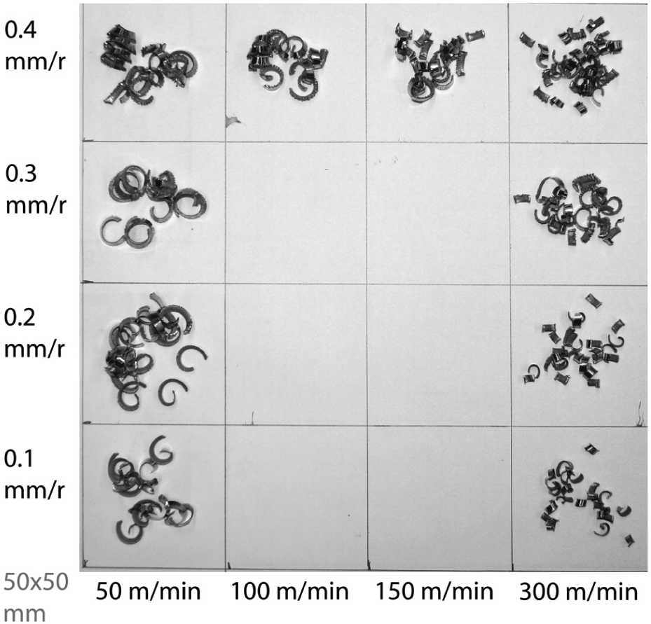
Experimental chip lengths at different cutting speeds and feed rates.
Discussion
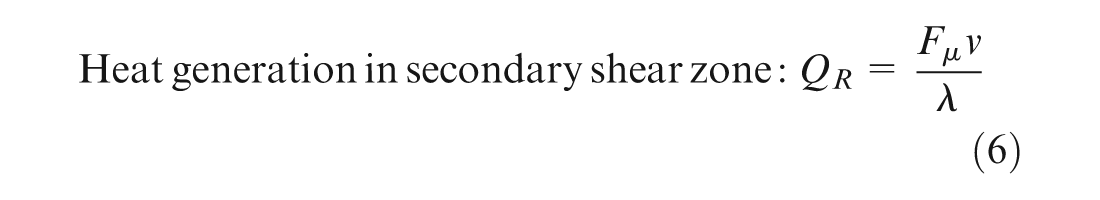
Smallest chip is formed in high cutting speed. This can be explained with the material testing results. Chip is ductile in high temperatures because low-lead brass is highly thermal softening. The softening effect is less drastic in high strain rates, so the chip forms more brittle in high cutting speeds. Other results can also be explained with chip temperature; therefore, heat generation in cutting is investigated. Heat generation during cutting is caused mainly by two factors: plastic deformation and friction between tool and chip. To control the cutting temperature, plastic deformation and friction should be minimized. If all mechanical works are assumed to turn into heat, then heat generation can be approximated by the following equations (5) and (6) where F and Fµ are the primary cutting force and friction force, v is cutting speed and λ is chip thickness ratio. To minimize heat generation, F and v should be minimized and λ maximized 33

To minimize cutting forces F and Fµ, a positive rake angle should be used.30,34 To reduce friction force, the contact area between tool and chip should be relatively low; this can be achieved by reducing cutting feed rate and/or cutting depth. Low feed is also beneficial for surface finish. 35 Also, as shown in the study by Astakhov, 29 as the normal stress at contact surface increases, the mean contact temperature is lower. 29 Additionally, reducing cutting feed increases the chip thickness ratio λ, as shown in Figure 13, and therefore reduces the heat generation in secondary shear zone. Values of chip thickness used for Figure 13 are presented in Table 2.
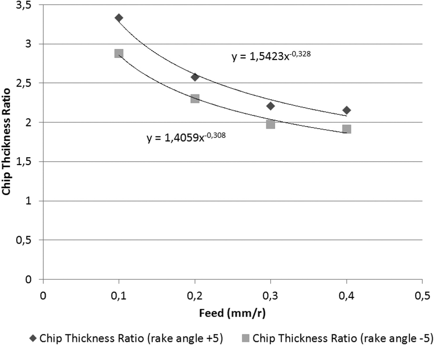
Chip thickness ratio.
Conclusion
Chip breakage of low-lead brass can be improved using high cutting speed, small feed rate and positive rake angle because of the following reasons: the material is thermal softening so the chip should stay as cool as possible for it to break. Positive rake angle leads to lower forces and therefore decreased heat generation. Cutting speed should be high, as the thermal softening effect is reduced in high strain rates. Low feed rate increases chip thickness ratio and decreases contact surface area. Increasing chip thickness ratio leads to lower heat generation. Reducing contact surface area using a chip breaking groove increases contact stress and therefore reduces cutting temperature. Also, cutting fluid with good cooling properties should be used to reduce cutting temperature. These observations were verified by FEM simulations and cutting experiments. It was observed that the material model used in this study was not able to predict the material behaviour in all temperature ranges.
Footnotes
Appendix 1
Chip breakage was not observed on any simulations with low cutting speeds (Figures 14–19). Simulations with average cutting speeds and positive rake angle show one near breaking point on lowest feed rate (Figures 20–22). No chip breaking was observed in simulations with medium cutting speed and negative rake angle (Figures 23–25). Simulations with high cutting speed and positive rake angle show chip breakage and near breaking points in low and medium feed rates (Figures 26–28). Near breaking points were observed in simulations with high cutting speed, negative rake angle and low or medium feed rates (Figures 29–31).
Declaration of conflicting interests
The authors declare that there is no conflict of interest.
Funding
This research received no specific grant from any funding agency in the public, commercial or not-for-profit sectors.