
Abstract
Micro-electrical discharge machining milling is a promising method to fabricate three-dimensional microshapes owing to its negligible cutting force and high-dimensional accuracy achievable. In order to machine intricate features, it requires the application of computer-aided manufacturing software to automatically generate the motion pattern for the electrode. Although most commercial computer-aided manufacturing systems cater for conventional milling, they cannot be directly applied for micro-electrical discharge machining milling due to the electrode wear issue and the existence of machining gap. This article presents these process-related issues and proposes an approach in customizing the conventional milling computer-aided manufacturing software for micro-electrical discharge machining milling of three-dimensional intricate shapes. The results show that it is feasible to utilize the current computer-aided manufacturing software to automatically generate tool paths for three-dimensional micro-electrical discharge machining milling by appropriately considering the tool wear and the inherent machining gap. In addition, further control parameters are also considered to achieve fine finish machining condition called simultaneous micro-electrical discharge/electrochemical milling. Different intricate three-dimensional microshapes are produced and evaluated to demonstrate the capability of this approach.
Introduction
A remarkable advantage of micro-electrical discharge machining (EDM) that makes it preferable for machining small-sized features is the negligible cutting force yielded by its noncontact material removal mechanism.1,2 In order to fabricate complex shapes by conventional EDM die-sinking, different intricate electrodes need to be prepared and repeatedly aligned on the machine spindle. However, this approach is problematic and impractical for micro-EDM, which involves the electrode smaller than few tens of microns in diameter.
In this scenario, contour micro-EDM milling has been proposed as a potential method to fabricate intricate three-dimensional (3D) shapes for micromold and die.3,4 In this method, the electrode in simple shapes moves along the preset tool path to remove material like the conventional micromilling. However, one challenging issue of micro-EDM milling is the inherent electrode wear. During machining, material is removed not only from the workpiece but also from the electrode itself, which has been known as electrode wear. As a result, the electrode loses its original size and shape, affecting the final dimensions of machined microfeatures. It has been reported that the electrode wear is composed of two factors, which are the corner wear and the bottom wear. 5 The bottom wear reduces the length of the electrode, whereas the corner wear changes its original shape. For micro-EDM drilling, by setting the drilled depth higher than the actual thickness of the workpiece, the electrode wear could be effectively compensated. However, in micro-EDM milling, the electrode wear must be resolved in different ways. When machining simple shapes such as microchannels or microslots of which the cross sections are identical, the electrode wear issue could be overcome by remachining the same slot using fresh electrode for a few times. 6 However, this approach seems to be inefficient for fabricating intricate 3D microshapes. To this end, uniform wear method, a prominent idea, has been proposed as an effective resolution for micro-EDM milling of complex 3D microshapes. 7 The primary objective of this method is to maintain the original shape of electrode. By removing the material layer-by-layer and conforming to some motion rules, the electrode shape is kept unchanged. Accordingly, the electrode wear is essentially lengthwise wear and thereby could be fully compensated in the longitudinal direction (along axis of electrode).
Aside from the electrode wear that has an apparent effect on the dimensional accuracy of machined microshape, the machining gap is also a noteworthy factor. Because of noncontact material removal mechanism, there exists a small distance between the electrode and the workpiece surface, which has been known as the spark gap. This fine gap is constituted of two components: the critical distance and the discharge distance. 8 Critical distance is the width that the dielectric fluid is breakdown and the sparks start to occur. Discharge distance is the depth of material layer removed by the sparks. Hence, this spark gap depends on the applied voltage, the energy of discharges, and it is also varied for different workpiece materials. Due to the stochastic nature of micro-EDM process, there has been no robust method that could precisely predict the machining gap. 9 As a result, it is usually determined by empirical approach. It can be up to hundred microns for EDM or could be as small as a few microns in micro-EDM. Although this few-micron gap is relatively small, it still has a significant effect on the final dimension of obtained microshapes of which the feature size is less than few hundred microns. 10
In the light of these reported studies, it could be seen that electrode wear and machining gap are two inherent and inescapable characteristics of micro-EDM milling that needs to be properly resolved during machining. In addition, when machining simple features like microslots, the machining code could be realized by a machine operator. However, for fabricating intricate 3D microfeatures such as partial spherical surface or sculptural shape, it is impractical to manually program the tool electrode motion. It requires the application of computer-aided manufacturing (CAM) software to automatically generate the motion pattern for electrode. Although many commercial CAM systems have been widely used in manufacturing industry for conventional milling process, such CAM module could not be directly applied for micro-EDM milling due to the existence of the aforementioned machining gap and electrode wear. While there are few attempts to develop the software in-house, there has been no dedicated CAM for micro-EDM milling that can be widely used for most commercial micro-EDM machine tools.11–13
This article presents a postprocessing approach to generate the tool paths for 3D micro-EDM milling based on the modification of current CAM software. It details the specific steps of the specially developed CAM-based tool path generation system that could be used with 3D micro-EDM milling as well as simultaneous micro-electrical discharge/electrochemical (ED/EC) milling (SEDCM milling). Experiments are then performed to demonstrate the capability of this approach.
Tool path generation system
Due to the existence of electrode wear, the existing commercial CAM module could not be directly applied for micro-EDM milling. In these commercial CAM systems that mainly cater for conventional milling, the tool shape and tool length are presumed to be unchanged during the entire machining process. Hence, it is required to be modified and developed for 3D micro-EDM milling. Figure 1 shows the tool path generation system used in this study, which has been developed based on the SolidWorks 14 and the ESPRIT CAM 15 environments. In this system, the compensation of machining gap is performed in the second step, whereas the electrode wear compensation is realized at steps 4, 5, and 6. The details of each step are given as below.
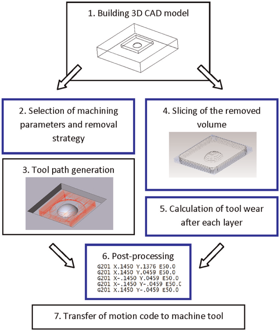
Tool path generation system.
Step 1: building 3D computer-aided design model
Prior to tool path generation, a 3D model of desired shape is built using the computer-aided design (CAD) environment. In this system, the CAD software used is SolidWorks 2011. This model is then used in the ESPRIT CAM as the targeted final shape to generate the tool path.
Step 2: selection of machining parameters and removal strategy
After the 3D CAD model has been transferred to the CAM system, different machining parameters are selected. First, the tool–workpiece gap must be determined. In contrast to conventional micromilling, micro-EDM is a noncontact machining process since there is a machining gap between the workpiece surface and the tool electrode. Hence, the generated tool paths need to account for this gap. Although the fine gap is merely a few microns in micro-EDM, this is essential to achieve the desired accuracy required for the dimensional scale of the microshapes. Therefore, aside from the radius of electrode, the offset distance in micro-EDM milling also involves the machining gap, as illustrated in Figure 2. Moreover, the machining gap also exists on its bottom side. Hence, the concept of virtual electrode is proposed. This virtual electrode is defined to be larger than the real electrode by the machining gap in all sides, as illustrated in Figure 3. By considering that the virtual electrode is being used instead of the real electrode, the process is considered to be similar to conventional micromilling except the electrode wear. Then, the machining strategy is selected based on the layer depth, the electrode overlap distance, and the horizontal scanning feedrate.
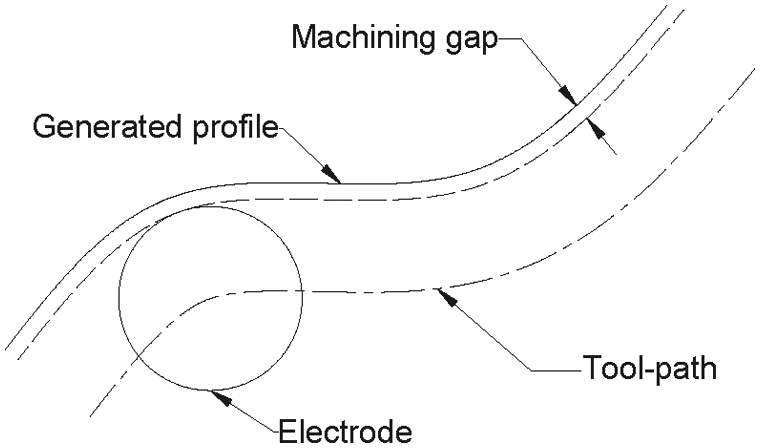
Tool path offset in micro-EDM milling.
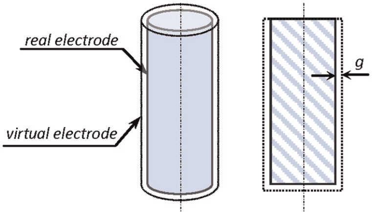
Concept of virtual electrode (g is the machining gap).
Step 3: tool path generation
In this step, the tool path is generated following the preset removal strategy using the ESPRIT CAM 2010. To maintain the original shape of the electrode, the electric discharge is intentionally kept to occur merely on the bottom side of the electrode, with a view to eliminating the corner wear. Hence, the material is removed layer by layer and the preset removal strategy needs to follow certain rules:
Small layer depth. 7 The depth of each layer must be smaller than the machining gap, as illustrated in Figure 4(a). When the layer depth is higher than the machining gap, as shown in Figure 4(b), the sparks occur not only on the bottom side but also on the lateral surface of tool electrode, resulting in the alteration of both electrode length and shape. Therefore, the layer depth is chosen to be smaller than the machining gap.
To-and-fro scanning, tool paths overlapping, and machining the inner part and the boundary alternately. 7 To remove the material of each layer, the electrode moves to-and-fro following the zigzag pattern to scan the entire area of each layer, as shown in Figure 5(a). To make the bottom of electrode wear more uniformly and to improve the accuracy of machined shape, the tool paths are overlapped and the material is removed from the boundary and the inner part alternatively.
Finish contouring. In contrast to square electrode, 7 when the cylindrical shape electrode is used, some materials on the boundary remain unmachined after to-and-fro scanning, as can be seen in Figure 5(a). Hence, after each layer, the electrode is required to move along the boundaries to remove these remaining materials for improving the accuracy of machined shape, as illustrated in Figure 5(b).
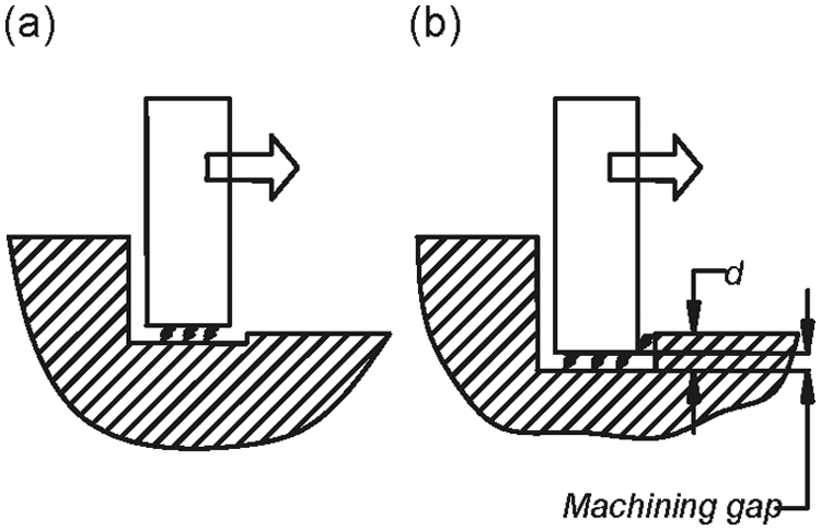
Electrode wear in micro-EDM milling: (a) bottom wear and (b) both bottom wear and corner wear (d is the depth of each layer).
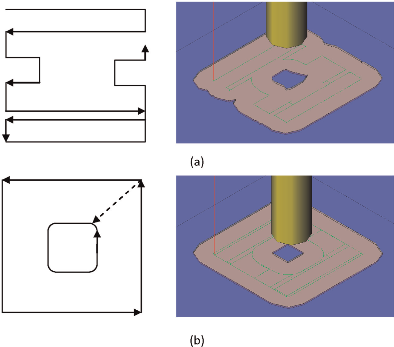
Tool path for every layer: (a) to-and-fro scanning and (b) finish contouring.
Step 4: slicing of the removed volume
As mentioned above, the conventional CAM software does not consider the electrode wear issue. Therefore, the electrode wear would be compensated during postprocessing. In order to have the electrode wear data, the longitudinal wear after every layer is determined based on the volume of that layer and the volumetric electrode wear ratio. Hence, in this step, the 3D CAD model of the removed volume is sliced into a series of layers. Then, the volume of each layer could be obtained.
Step 5: calculation of electrode wear after each layer
Based on the volume of each removed layer obtained from the previous step, the length wear after that layer could be calculated as follows
where σ is the electrode–workpiece volumetric wear ratio, Vi is the volume of the layer i, and Ae is the cross-sectional area of the electrode.
Step 6: postprocessing
This step involves the translation from tool path pattern to motion program for the machine tool. After the preliminary machining program has been generated, the iteration is used to compensate for the longitudinal electrode wear after each layer. The new Z coordinate of layer i + 1 is determined as follows
where d is the preset layer depth and Δli is the longitudinal wear after the layer i.
Step 7: transfer of program to the machine tool
After postprocessing, the final motion program is downloaded to the controller of EDM machine tool. The machining process is then started to fabricate the desired microshapes. The electrode moves according to the generated tool path to remove the material layer by layer.
Experimental details
In order to demonstrate the capability of the presented approach, experiments were conducted to fabricate different intricate microshapes and analyze their dimensional accuracy.
Machine setup
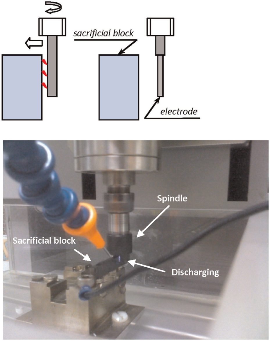
The experimental works were performed on the multiprocess machine tool DT-110 manufactured by Mikrotools. 16 The apparatus is illustrated in Figure 6. The machine tool has a resolution of 0.1 µm and repeatability of 1 µm for all axes. Table 1 shows the machining conditions of micro-EDM milling process, whereas Table 2 exhibits the main parameters determining the tool path strategy. In this study, deionized (DI) water was used as the machining fluid because it yields lower tool wear rate compared with hydrocarbon oil. However, the usage of DI water could lead to the excessive material dissolution, which has been reported to affect the machining accuracy. Hence, a specially developed short voltage pulse generator was used to suppress the material dissolution. 17 Obtaining from the preliminary tests, the electrode wear rate is found to be around 1.1% for the machining conditions used in this study.
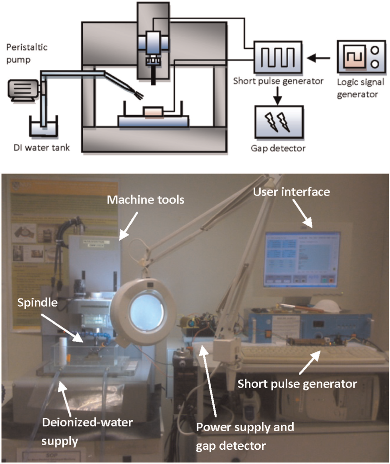
Experimental apparatus.
Machining conditions.
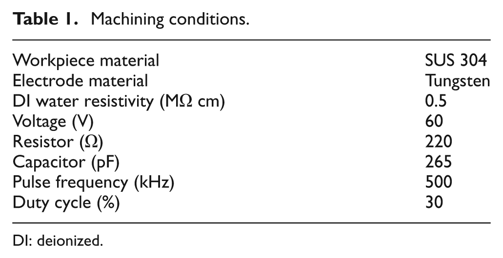
DI: deionized.
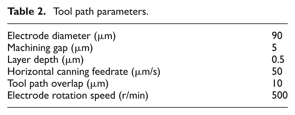
Tool path parameters.
Electrode preparation
The handling and mounting of the electrode on the machine spindle tend to incur a clamping error, which results in the electrode eccentricity, especially when the electrode size is less than few hundred microns. 4 This clamping error emerges as a significant amount in micro-EDM. Hence, for improving the dimensional accuracy of obtained shapes, the electrode used in micro-EDM milling needs to be on-machine fabricated to eliminate this eccentricity.
In this study, the new horizontal block-electrodischarge-grinding (BEDG) is proposed to reduce the electrode diameter and thus eliminate the eccentricity induced by clamping error. As illustrated in Figure 7, a tungsten carbide block is used as a sacrificial electrode. After setting the zero point, the electrode is moved horizontally toward the sacrificial block for a certain distance. The sparks occur and the material is removed from the electrode, resulting in the reduction of its diameter. The procedure is repeated until the desired diameter of the electrode is obtained. This method is different from the reported studies 18 in such a way that the feeding is given in the horizontal direction instead of the vertical direction. Using this approach, after being clamped on the machine spindle, the tungsten electrode diameter was reduced from ∅200 to ∅90 µm.
Horizontal block-electrodischarge-grinding.
For demonstrating the existence of the eccentricity induced by clamping error, Figure 8(a) shows the microscopic image of the fabricated electrode taken by the camera integrated on the machine tool. It can be seen that the distances between the original surface and the newly formed surface of electrode are different for the left and right side. It shows that the central axis of electrode and machine spindle is not concentric. In addition, Figure 8(b) exhibits the image of sacrificial block after machining. For the all four steps, the feeding depth is set to be identical 30 µm. Accordingly, the width and depth of the wear mark should decrease from the first to the last step. This is found to be valid from the second step to the fourth step. However, the first wear mark is observed to be shallower and smaller compared with the mark of the second step. This probably stems from the eccentricity of the electrode after clamping. Hence, it implies that that the elimination of this eccentricity is important to improve the dimensional accuracy of fabricated shapes.
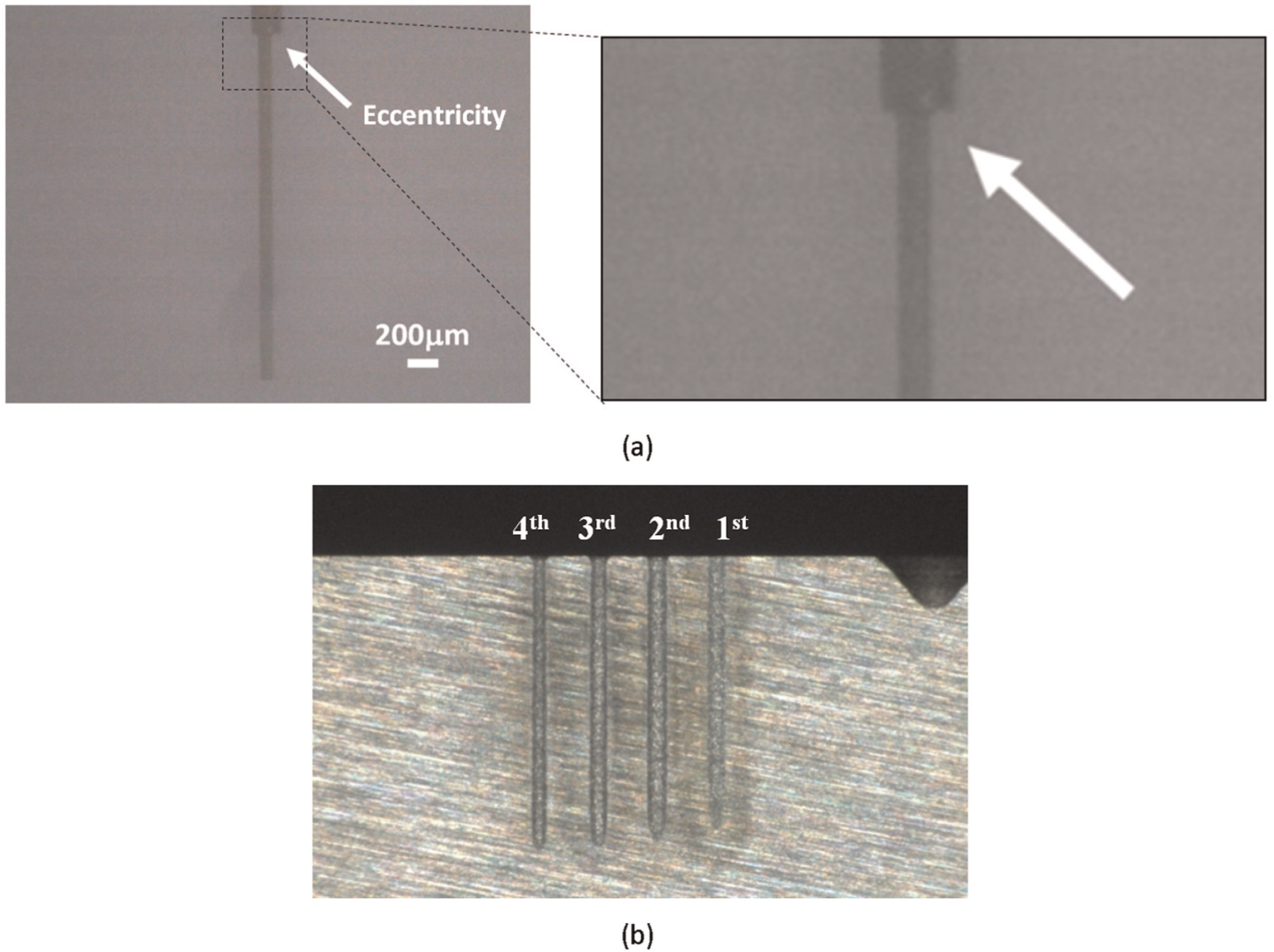
(a) Electrode and (b) the sacrificial block after machined by horizontal BEDG.
Measurements
After machining, the scanning electron microscope (SEM) JSM-5500 was used to capture the micrographs of the machined shapes. Their 3D surface profiles were measured using the NANOVEA noncontact profilometer PS-50 equipped with the chromatic confocal sensor CHR-150. 19
Fabrication of the intricate 3D microshapes
Figure 9 shows the 3D-view and top-view SEM images of the machined microcavity in the form of a five-petal flower, which demonstrates the capability of the developed CAM system in fabricating intricate shapes. It should be highlighted that each of the five petals is formed by curved surfaces inclined above the horizontal. Such a complex cavity is infeasible to be fabricated without the development of a CAM system to automatically generate the compensated electrode motion program. Figure 10 outlines the 3D surface profile of the obtained micro-flower, revealing the good flatness and integrity of the fabricated shape.
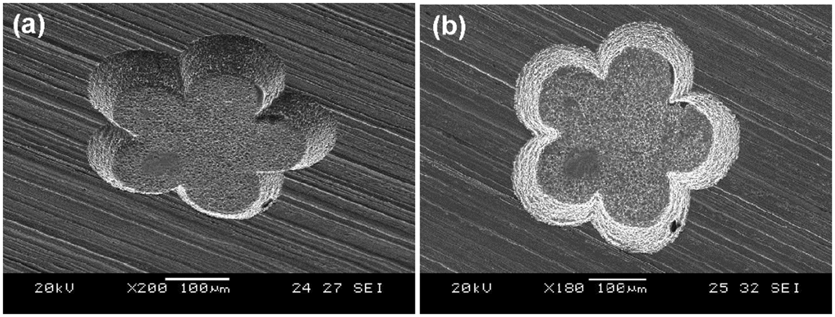
SEM micrographs of intricate microcavity: (a) 3D view and (b) top view.
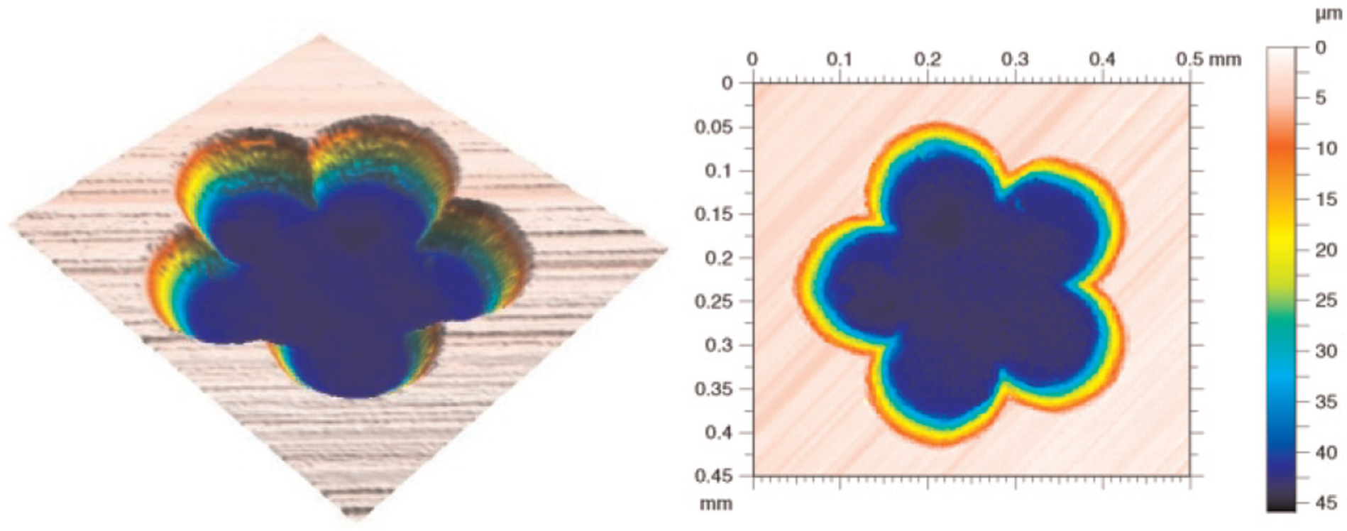
Three-dimensional surface profiles of the fabricated intricate microcavity.
Efficiency of machining gap and electrode wear compensation
In order to demonstrate the effect of machining gap and electrode wear compensation on the dimensional accuracy, experiments were carried out to fabricate the microcavity with the dimensions showed in Figure 11. It has the size of 0.4 mm × 0.4 mm × 0.05 mm. Two sets of this microcavity were fabricated. In the first set, neither the machining gap nor the electrode wear is considered. Accordingly, the electrode is defined following its real dimension. The z-axis coordinate of each layer is also not amended. In contrast, for the second set, the virtual electrode is defined using the aforementioned method, and the new z-axis coordinate of each layer is updated based on the electrode wear data calculated.
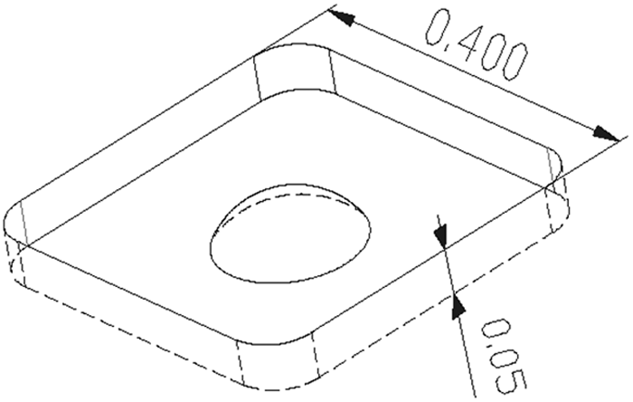
3D CAD model of sample microcavity.
Effect of electrode wear compensation
Figure 12 shows the SEM images of obtained microcavity and the 3D profiles of the two sets are plotted in Figure 13. From Figure 13(a) in which the electrode wear is not taken into account, it could be observed that the depth of the machined microcavity is around 35 µm only, which is significantly deviated from the 50 µm desired depth. This demonstrates the effect of electrode wear during machining on the final dimension of fabricated shape. Although the layer-by-layer removal strategy is effective in maintaining the original electrode shape, the length wear must be appropriately compensated to obtain the target depth of the microcavity. Without the electrode wear compensation, the electrode becomes shorter after removing a layer and it induces an error in z-axis coordinate of the electrode tip. This systematic error is cumulative after each layer, and it becomes as high as 15 µm for the entire machining process in this case.
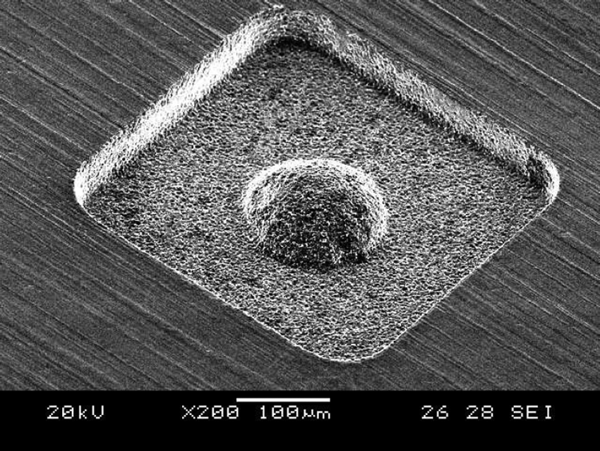
SEM image of machined microcavity.
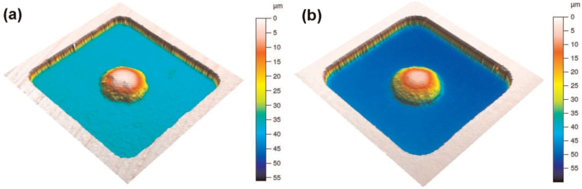
The 3D surface profiles of fabricated microshapes: (a) without electrode wear and machining gap compensation and (b) with electrode wear and machining gap compensation.
Hence, the z-axis coordinate of the electrode tip needs to be updated through the length wear compensation before it starts to remove a new layer. The longitudinal wear of the electrode after each layer is thus calculated using the procedure described above. It should be highlighted that with the compensation of the electrode wear after each layer, the depth of the obtained microcavity is found to increase to nearly 50 µm, which is the desired final dimension, as indicated in Figure 13(b). This demonstrates that the longitudinal wear compensation is crucial in achieving high geometrical accuracy of 3D micro-EDM milling. It also shows that the developed tool path generation system is effective in compensating the electrode length wear during machining.
Effect of machining gap compensation
In micro-EDM, there is no direct contact between the electrode and the workpiece, and thus they are separated by the machining gap. Although this fine gap width is within a few microns, it may affect the dimensional accuracy of the final machined shape, especially in micromachining where the feature size is less than few hundred microns. Figure 14(a) shows the cross-sectional profile of the machined surface without the consideration of machining gap. During the tool path generation, the tool offset is defined based on its actual diameter. It can be observed that the width of the fabricated cavities is about 410 µm, which is larger than the desired dimension by 10 µm. This deviation is found to be equivalent to 2 times of the 5 µm machining gap, which was determined in the preliminary study. Using the virtual electrode concept to compensate for the machining gap, the width of the obtained microshape is found to be approximately 400 µm, which is the desired dimension, as plotted in Figure 14(b).
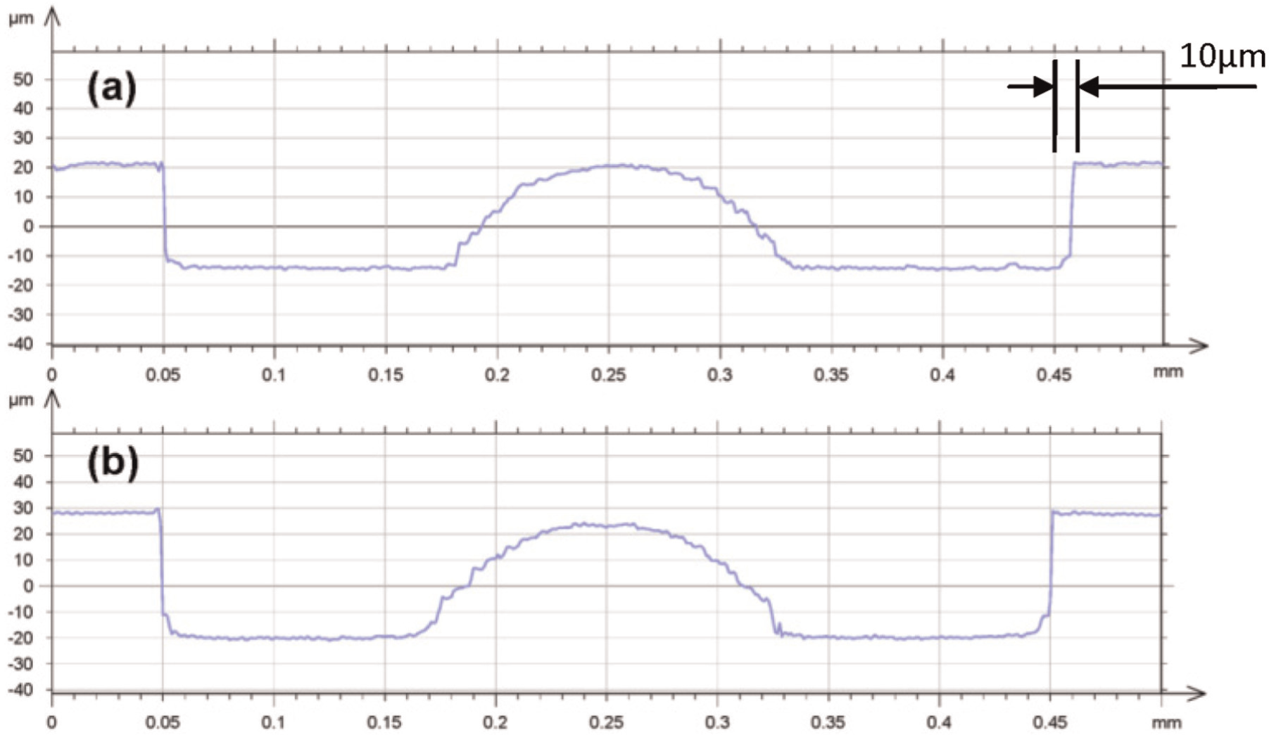
Cross-sectional profiles of fabricated microshapes: (a) without electrode wear and machining gap compensation and (b) with electrode wear and machining gap compensation.
Similarly, with the appropriate compensation of longitudinal electrode wear and the machining gap, the microcavity formed by four inclined planes with relatively good dimensional accuracy is also obtained, as showed in Figure 15. This indicates that machining gap compensation is also a prime factor for obtaining high-dimensional accuracy in micro-EDM milling, and it must be considered during electrode definition and tool path generation.
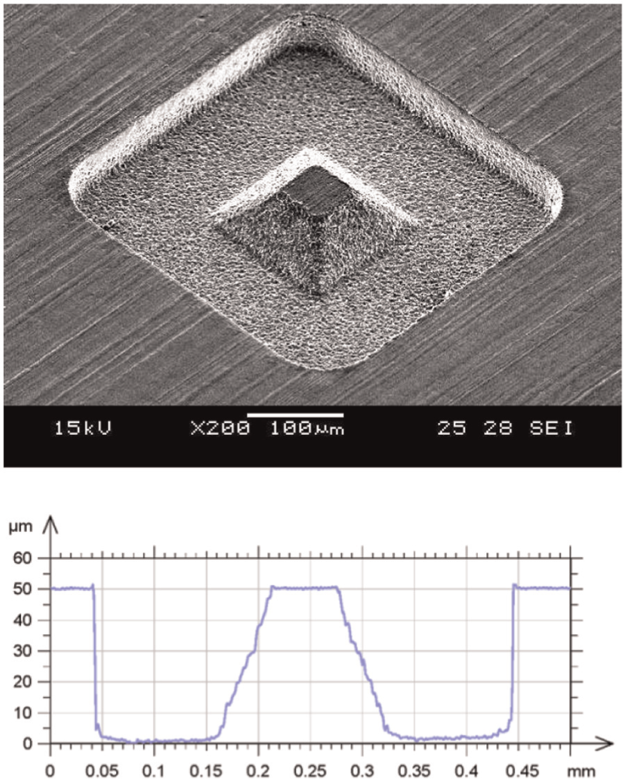
SEM image and cross-sectional profilograph of the obtained microcavity.
Application in SEDCM milling
It should be highlighted that the surface of microshapes is formed by the overlapping of discharge craters, as can be seen in Figures 9 and 12. Therefore, it associates with high surface roughness. 20 This stems from the noncontact removal mechanism of micro-EDM in which the material is removed by electric sparks through melting and vaporization. Recently, SEDCM milling has been presented as an effective method to fabricate microshapes with enhanced surface integrity. 21 The working principle of this hybrid machining process is summarized in Figure 16. In SEDCM milling, the electrochemical reaction is exploited to remove the affected layer on the micro-EDMed surface, whereby its finish is improved. Low-resistivity DI water is used as a bicharacteristic fluid to facilitate material removal by both electric discharges and electrochemical reaction in the same machining process. By using a suitable feedrate, the electrochemical reaction is promoted for better surface finish, whereas short voltage pulses are applied to localize material dissolution for ensuring dimensional accuracy.
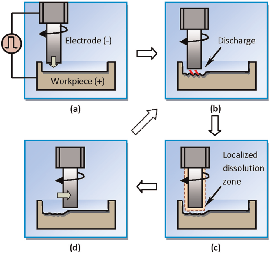
Simultaneous micro-ED/EC milling: 21 (a) vertical feeding, (b) discharge, (c) dissolution, and (d) horizontal feeding.
Hence, an attempt has been made to apply the presented CAM system in SEDCM milling with the aim to obtain the microshapes with better surface finish. Experiment works were performed to fabricate the similar microcavities discussed above. In order to attain the SEDCM milling condition, the material was removed in a layer of 1 µm thickness and the horizontal scanning feedrate was adjusted to 5 µm/s. Figure 17 shows the SEM micrographs of the microshapes fabricated under two different regimes, which are micro-EDM milling and SEDCM milling, respectively. Compared with micro-EDM milling, it can be observed that SEDCM milling yields better surface finish. Overlapped discharge craters are found on the surface generated by micro-EDM milling but very few on the surface obtained by SEDCM milling, as shown in Figure 17. Accordingly, the average surface roughness Ra is also lowered from about 0.176 (in micro-EDM milling) to 0.027 µm (in SEDCM milling). This indicates that the developed CAM system could also be directly applied in SEDCM milling to obtain complex 3D microshapes with enhanced surface finish. To investigate the accuracy of machined features, the profiles of obtained microshapes are compared with the ideal profile, as plotted in Figure 18. The average profile error in case of micro-EDM milling is around 1.9 µm, whereas it is about 2.2 µm for SEDCM milling.
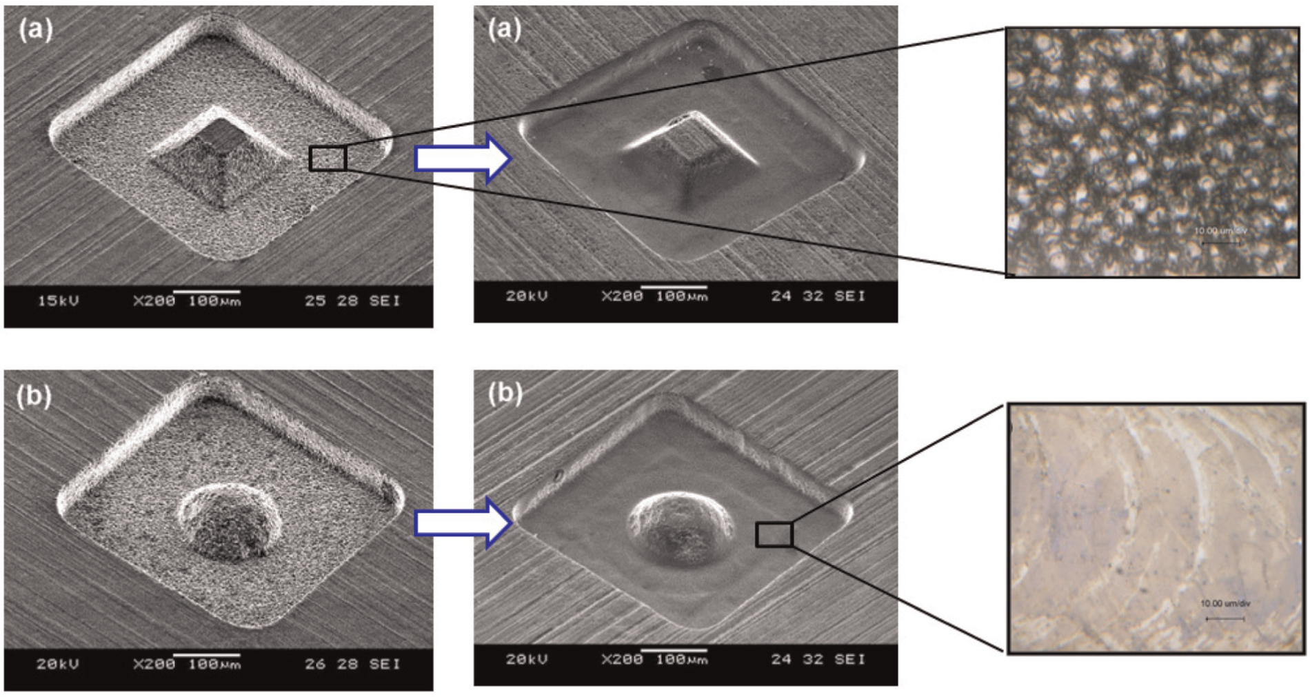
SEM images of microshapes fabricated under micro-EDM milling and SEDCM milling regimes: (a) micropyramid and (b) microdome.
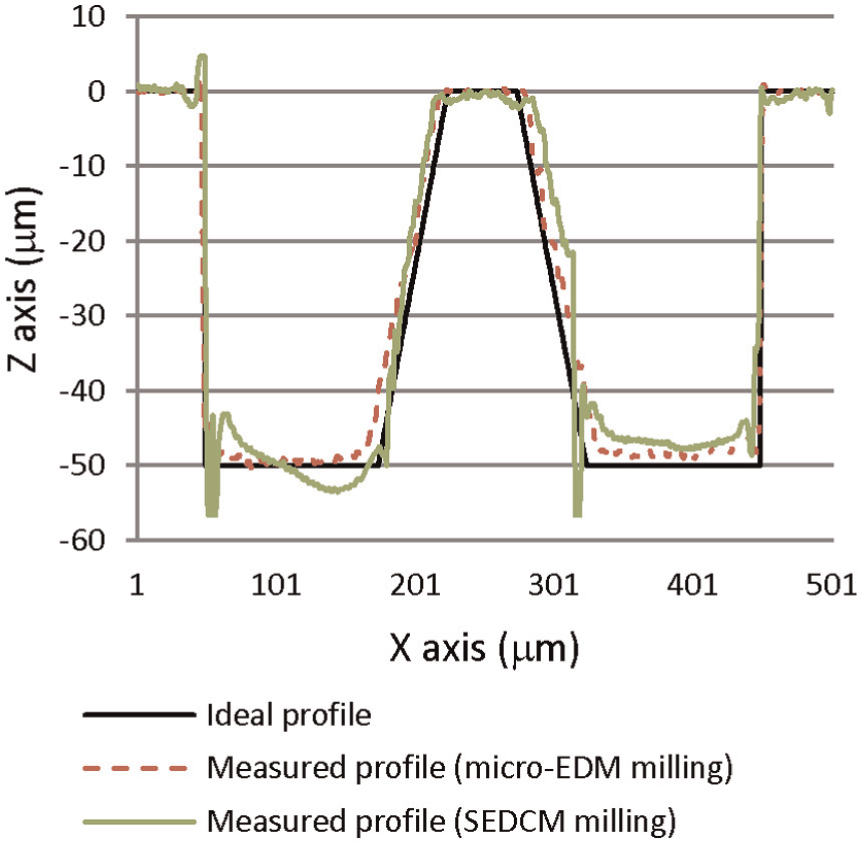
Measured profiles of microshapes machined by micro-EDM milling and SEDCM milling.
Conclusion
This article presents an approach to customize current CAM software for 3D micro-EDM milling and its application in SEDCM milling. Different microshapes have been produced to demonstrate the capability of the proposed system. The following conclusions could be drawn from this study:
Machining gap and electrode wear are two process-related issues that need to be resolved for micro-EDM milling of intricate 3D microshapes.
By using the virtual electrode model to compensate for machining gap and implementing the electrode wear compensation in the tool path generation system, dimensional accuracy of the obtained microshapes has been improved to great extent.
When the cylindrical electrode is used, finish contouring needs to be added into the tool path for improving the accuracy of machined shapes.
Clamping of small-sized electrode on machine spindle induces the eccentricity that influences the final dimension of microshapes. The new horizontal BEDG has been presented to on-machine fabricate electrode and thus eliminate this eccentricity for better control of dimensional accuracy.
The presented approach is also directly applicable to SEDCM milling for fabricating 3D microshapes with enhanced surface finish.
Footnotes
Declaration of conflicting interests
The authors declare that there is no conflict of interest.
Funding
This research received no specific grant from any funding agency in the public, commercial, or not-for-profit sectors.