
Abstract
This research work explores the relationship of machining parameters such as pulse on time (Ton), pulse off time (Toff), peak current (Ip), spark gap voltage, wire feed and wire tension on the material removal rate, wire wear ratio and surface roughness for pure titanium in wire electric discharge machining process. The Box–Behnken design had been utilized to plan the experiments, and response surface methodology was employed for developing the empirical models. The peak current, spark gap voltage, pulse on time, pulse off time and interaction between pulse on time and peak current affected the surface roughness significantly. Multi-response optimization of process parameters was obtained using desirability approach. Furthermore, the selected machined samples were analyzed using energy-dispersive X-ray analysis, scanning electron microscope and X-ray diffraction techniques. The predictions from this model were validated by conducting confirmatory experiments.
Keywords
Introduction
The use of light, thin and compact mechanical elements has recently become a global trend. The search for new, lightweight material with greater strength and toughness has led to the development of new generation of materials such as titanium. Although their properties may create major challenges during machining operations, having greater hardness and reinforcement strength, these materials are difficult to machine by the traditional methods. Although these materials can be machined conventionally, subsurface damages such as metallurgical alterations, work hardening and microcracks can occur. Since the cost of using conventional machining is generally prohibitive, nonconventional machining such as wire electric discharge machining (WEDM) is the ideal technique in dealing with these materials. 1 Titanium is alloyed with aluminum, manganese, iron, molybdenum and other metals to increase strength, to withstand high temperatures and to lighten the resultant alloy. Titanium’s high corrosion resistance is also a valuable characteristic. When exposed to the atmosphere, titanium forms a tight, tenacious oxide film that resists many corrosive materials. Titanium and its alloys are classified as difficult-to-machine materials. Machining of titanium is generally done by the conventional processes of machining keeping very low feed to ensure that during machining there are the least structural changes. The problems of machining characteristics for titanium and its alloys with conventional machining processes are summarized below: 1
Titanium and its alloys are poor thermal conductors. As a result, the heat generated when machining titanium cannot dissipate quickly; rather, most of the heat is concentrated on the cutting edge and tool face.
During machining, titanium alloys exhibit thermal plastic instability that leads to unique characteristics of chip formation. The shear strains in the chip are not uniform; rather, they are localized in a narrow band that forms serrated chips.
The contact length between the chip and the tool is extremely short (less than one-third the contact length of steel with the same feed rate and depth of cut). This implies that the high cutting temperature and the high stress are simultaneously concentrated near the cutting edge (within 0.5 mm).
Serrated chips create fluctuations in the cutting force; this situation is further promoted when alpha–beta titanium carbide and titanium nitride coatings are not suitable for machining titanium alloys because of their chemical affinities.
Most cryogenic machining studies on titanium and its alloys have documented improved machinability when freezing the workpiece or cooling the tool using a cryogenic coolant. However, inherent weaknesses exist in these approaches.
Therefore, there is a crucial need for reliable and cost-effective machining processes for titanium and its alloys. Keeping in view the difficulties associated with conventional machining of titanium, this work is an attempt toward machining of the same with WEDM. The work revealed that WEDM could be successfully applied for the machining of titanium alloys. WEDM is a specialized thermal machining process capable of accurately machining parts with varying hardness or complex shapes, which have sharp edges that are very difficult to be machined by the main stream machining processes. This practical technology of the WEDM process is based on the conventional EDM sparking phenomenon utilizing the widely accepted noncontact technique of material removal. Since the introduction of the process, WEDM has evolved from a simple means of making tools and dies to the best alternative of producing microscale parts with the highest degree of dimensional accuracy and surface finish quality. Some of the common applications of WEDM are including the fabrication of the stamping and extrusion tools, dies, fixtures, gauges, prototypes, aircraft, medical parts and grinding wheel form tools. 2 The material removal mechanism of WEDM is very similar to the conventional EDM process involving the erosion effect produced by the electrical discharges (sparks). In WEDM, material is eroded from the workpiece by a series of discrete sparks occurring between the workpiece and the wire, separated by a stream of dielectric fluid, which is continuously fed to the machining zone. In the case of WEDM, a wire electrode is trailing vertically through the workpiece, which usually is fed horizontally. This process utilizes a continuously traveling wire electrode made of thin copper, brass or tungsten of diameter 0.05–0.3 mm, which is capable of achieving very small corner radii.3,4 The wire is kept in tension using a mechanical tensioning device reducing the tendency of producing inaccurate parts. During the WEDM process, the material is eroded from the workpiece by a series of discrete sparks, ahead of the wire. The microprocessor used to continuously feed thin wire will constantly maintain the gap (0.025–0.05 mm) between the wire and the workpiece. In WEDM process, there is no direct contact between the workpiece and the wire, thus eliminating the mechanical stresses during machining.
Past research work
Miller et al. 5 presented a study for the optimization of cutting parameters and were effective for material removal rate (MRR) and surface finish. The surface finish increased on with increasing the discharge current, pulse duration and wire speed. Huang and Liao 6 studied the uses of gray relational and signal-to-noise ratio for demonstrating the influence of table feed and pulse on time on the MRR. Hewidy et al. 7 modeled the electrical parameters of WEDM of Inconel-601 using response surface methodology. It was concluded that the volumetric metal removal rate generally increased with the increase of the peak current value and water pressure. Mahapatra and Patnaik 8 optimized the parameters using Taguchi method on D2 tool steel as work material in WEDM process. It was observed that discharge current, pulse duration, dielectric flow rate and the interaction between discharge current and pulse duration were the most significant parameters for cutting operation. Mathematical models were developed for optimization of MRR and surface finish using nonlinear regression and genetic algorithm method. Ramakrishnan and Karunamoorthy 9 enumerated the Taguchi’s robust design approach for optimizing MRR, surface roughness and wire wear ratio (WWR). Manna and Bhattacharya 10 modeled the machining parameters using the dual Taguchi and Gauss elimination method. The investigation results accomplished that the voltage and Ton were the momentous parameters for controlling the MRR. Sarkar et al.11,12 investigated the machining characteristics of γ-TiAl in single- and multi-pass cutting operation. Yang et al. 13 proposed the hybrid modeling method for cutting of pure tungsten. Kumar et al. 14 explored the study on WEDM in machining of commercially pure titanium. Shah et al. 15 investigated seven machining parameters in addition to varying material thickness on performance measures such as MRR, kerf and surface roughness on tungsten carbide samples machined by WEDM. The design of experiments was based on Taguchi orthogonal designs. Results showed the little effect of varying material thickness on MRR and kerf. Sadeghi et al. 16 discussed the effects of process parameters on surface roughness and metal removal rate in WEDM of AISI D5 steel alloy. It was found that discharge current and pulse interval were more significant for MRR and surface roughness than open circuit voltage. Kung and Chiang 17 studied behavior of WEDM of aluminum oxide–based ceramics. The effects of machining parameters on MRR and surface roughness were evaluated. Tzeng et al. 18 analyzed the dependence of the MRR and workpiece surface finish on process parameters during the manufacture of pure tungsten profiles by WEDM. A hybrid method including a back-propagation neural network, a genetic algorithm and response surface methodology was proposed to determine optimal parameter settings of the WEDM process. The results showed that the advanced computing methods were effective tools for the optimization of WEDM process parameters. Rao and Pawar 19 proposed the mathematical models using response surface modeling (RSM) for correlating the interrelationships of various WEDM parameters for machining speed and surface roughness. Yu et al. 20 explored the study on polycrystalline silicon material using WEDM process to optimize the groove width, surface roughness and cutting speed. The results showed that pulse on time was the most significant factor for cutting speed, surface roughness and groove width. Kuruvila and Ravindra 21 investigated the WEDM parameters on the hot die steel for dimensional error, surface roughness and MRR. The study revealed that smaller pulse off time and pulse on time resulted in improving the overall performance with minimum dimensional error and good surface finish.
This research work explores the machining characteristics of pure titanium. The six parameters, that is, Ton, Toff, Ip, spark gap voltage (SV), wire feed (WF) and wire tension (WT), are mottled to explore their effects on performance measures, that is, MRR, WWR and surface roughness. In addition, a second-order polynomial regression model, in terms of machining parameters, has been developed using response surface methodology. These responses are optimized using multi-objective optimization through desirability.
Experimental methodology
The experiments were performed on a four-axis computer numerical control (CNC)-type wire electric discharge machine as shown in Figure 1(a). The six parameters, that is, Ton, Toff, Ip, SV, WF and WT, were varied to investigate their effect on output responses, that is, the MRR, WWR and surface roughness. The parameters reserved constant during machining were electrode (brass wire with 0.25 mm diameter), thickness (26 mm) and dielectric pressure (7 kg/cm2). The chemical composition of work material is taken for experimentation work as follows: carbon 0.10%, nitrogen 0.03%, oxygen 0.25%, hydrogen 0.015%, iron 0.30% and titanium 99.03%. The work material in the form of square plate having dimensions 148 mm (length) × 148 mm (width) × 26 mm (thickness) was in use for the experimentation work. The machining rate was measured in millimeter per minute and surface roughness in micrometers. The surface roughness was measured using the Mitutoyo’s SURFTEST model, SJ-301. Figure 1(b) and (c) shows the work path and job profile during machining.
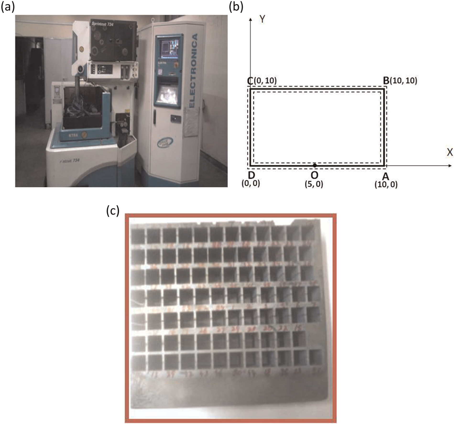
Job profile and experimental setup of WEDM machine tool. (a) WEDM CNC type, Electronica Sprintcut-734 machine tool, (b) Work-path profile and (c) square punch produced after WEDM.
Experimental design
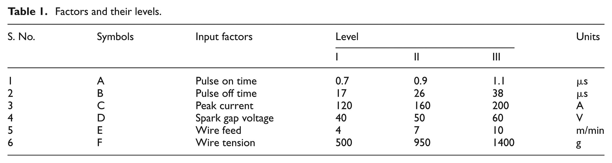
The process parameters and their levels for the main experiments were decided on the basis of the pilot experiments conducted using one-factor-at-a-time approach as shown in Table 1. The Box–Behnken design (BBD) was used for planning and executing the subsequent main experimentation, as shown in Table 2. In this study, an effort has been made to model the empirical relationship between machining parameters by using response surface methodology. Response surface methodology is a collection of mathematical and statistical techniques that employ regression analysis to provide a relationship between the input process parameters and output performance based on experimental results. Finally, the analysis was done to study the main effects and their interactions to explore the quadratic effects of the influence of parameters on the performances. A quadratic model relating the response to the factors for BBD is governed by the following relation
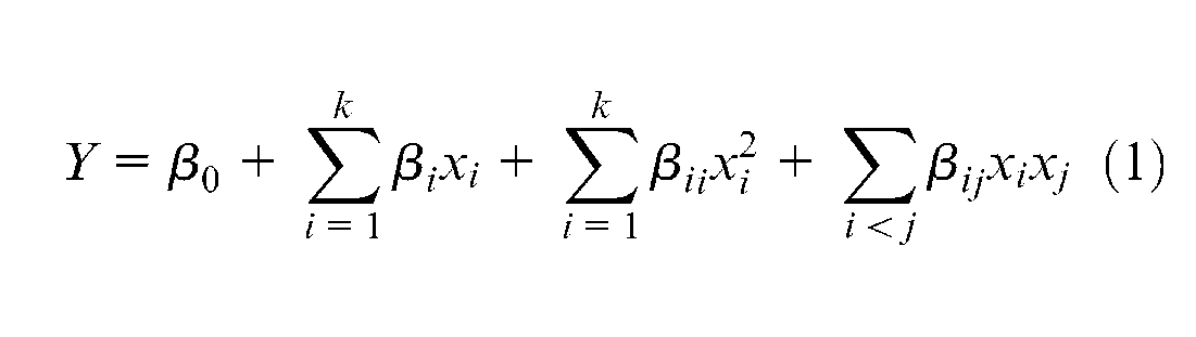
where Y is the preferred response, xi (1, 2, …, k) are the independent k quantitative process variables, β0 is a constant and βi, βii and βij are the coefficients of linear, quadratic and interaction terms, respectively.
Factors and their levels.
Experimental design and results.
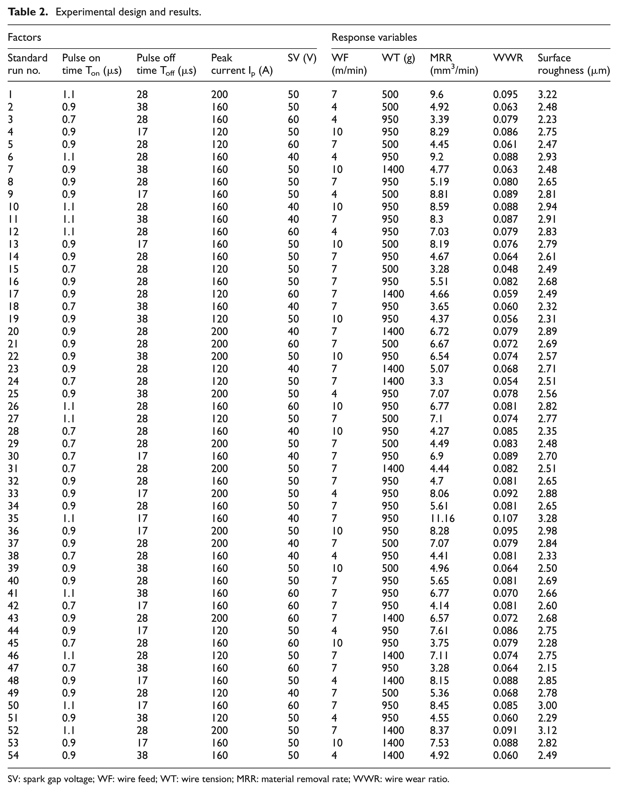
SV: spark gap voltage; WF: wire feed; WT: wire tension; MRR: material removal rate; WWR: wire wear ratio.
Results and discussion
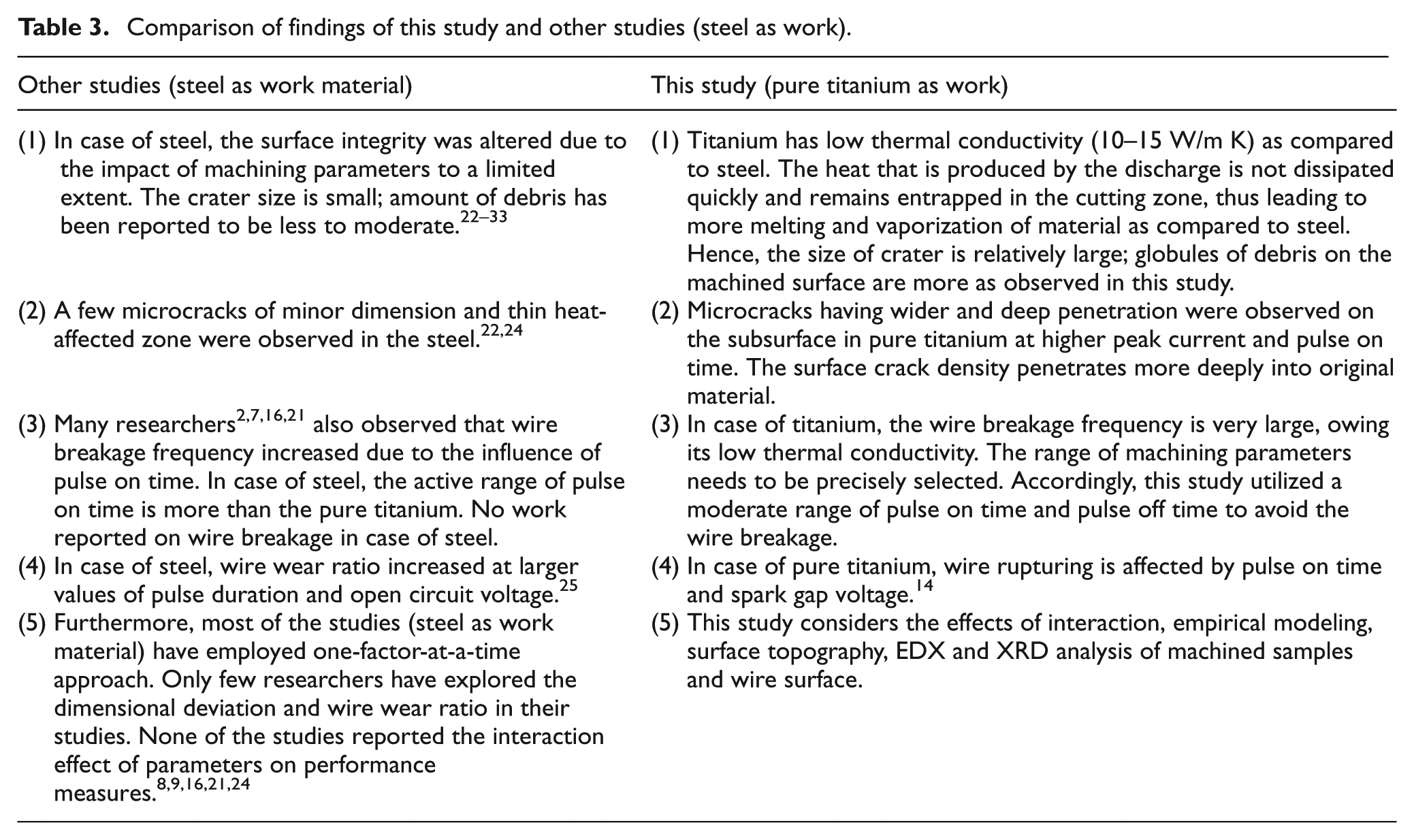
From the application point of view, WEDM is a more suitable candidate for machining of titanium as compared to machining of other materials such as steel, as steel can be easily machined using conventional machining. A detailed comparison of WEDM characteristics of pure titanium (in this study) and other materials (such as steel) as reported by other researchers in the literature was difficult to make because all these studies have been reported to make use of different WEDM setups involving different range of machining parameters. However, a summarization of machining characteristics of titanium and steel is done and is presented in Table 3.
Comparison of findings of this study and other studies (steel as work).
Effect of process parameters on MRR
The effect of the process variables on the MRR has been determined as follows
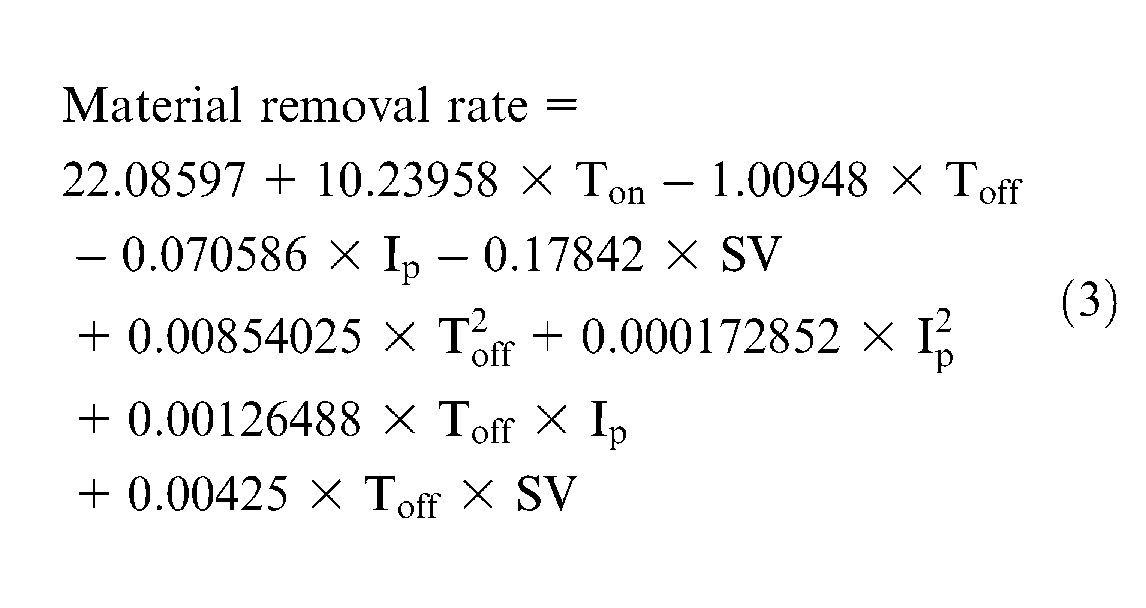
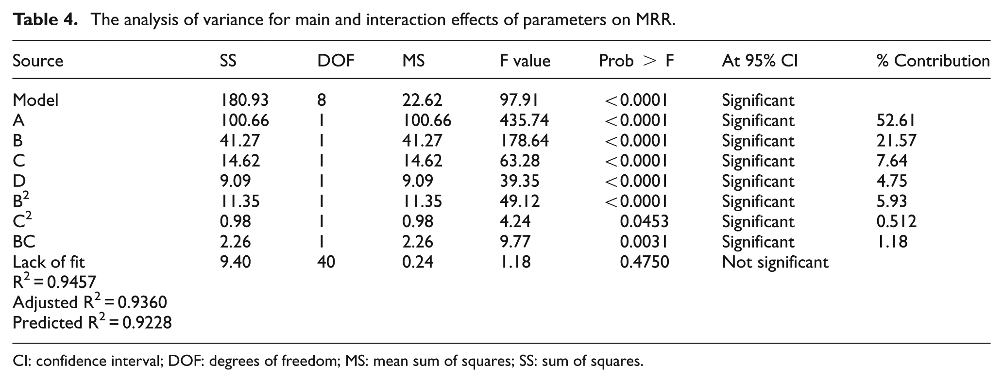
where MR = machining rate in mm/min, b = width of cut in mm and t = height of workpiece in mm. Design expert 6.0 software was used to compute the values as shown in Table 2. The adequacy of model and effects of process parameters with their interactions for MRR have been shown in Table 4. This model was developed for 95% confidence level. The model F value of 97.91 implied that the model is significant for MRR. It was observed from the F and P values that the factors A (Ton) and B (Toff) have more significant effect on MRR. The values of “Prob > F” less than 0.05 indicates that the model terms are significant. In this case, A, B, C, D, BC, BD, B 2 and C 2 are significant model terms. The lack of fit F value of 0.4750 implies that it is not significant compared to pure error. The “Pred. R2” of 0.9228 is in sensible agreement with the “Adj. R2” of 0.9360. This model can be used to navigate the design space. The model for MRR is given by
The analysis of variance for main and interaction effects of parameters on MRR.
CI: confidence interval; DOF: degrees of freedom; MS: mean sum of squares; SS: sum of squares.
Figure 2(a)–(f) shows the three-dimensional interaction response surfaces and contour plots for the response MRR. From the contour plot and response surface, it was observed that MRR varies from 4.91 to 7.70 mm3/min with the increase in peak current from 120 to 200 A and decrease of Toff from 38 to 17 µs. It was observed from the plots Figure 2(a)–(c) that MRR increases on increasing the peak current and decreasing pulse off time. This can be explained on the basis of increase in the rate of discharge energy and decrease in pulse frequency taking place while the peak current is increased or pulse off time is decreased. The concentration of discharge energy in the spark gap leads to rapid melting and vaporization of molten metal and floating metal suspended in the electrical discharge, which leads to increment in the MRR.26,27 High peak current and low pulse off time increase the amount of debris in the spark gap, which leads to abnormal arcing. The abnormal arcing reduced the dielectric strength, thereby resulting in wire breakage, particularly when the value of peak current was increased beyond 200 A. Figures 3 and 4 show the surface topography of the machined surface of titanium samples, obtained by using scanning electron microscope (SEM). From the examination of surface texture, it could be observed that during WEDM, the molten material is deposited in the form of globules of debris. Also, there is a significant variation in the crater size, which could be related to the uneven distribution of discharge energy along the surface. From the previous studies, it is established that all the molten metal cannot be removed from the gap and some part of this molten metal solidifies on the surface machine samples, known as recast layer. Appearance of significant recast layer is shown in Figure 5. It could be very well established from Figure 5 that the extent (thickness) of recast layer is much less than other machining methods such as die sinking electric discharge machining, while machining titanium. Figure 2(d)–(f) shows the interaction and contour surface plots. It was observed from the plots that MRR increases (from 4.91 to 7.70 mm3/min) with the decrease in pulse off time and SV. It was found that by decreasing the SV, the wire speed increases that leads to increase in the MRR. This study revealed that higher MRR is achieved at the lowest SV, lower pulse off time and high peak current. Figure 2(g)–(i) displays the normal probability plot of residuals and residual versus predicted plots for MRR. It was observed that the residuals generally fall on a straight line implying that the errors are normally distributed.
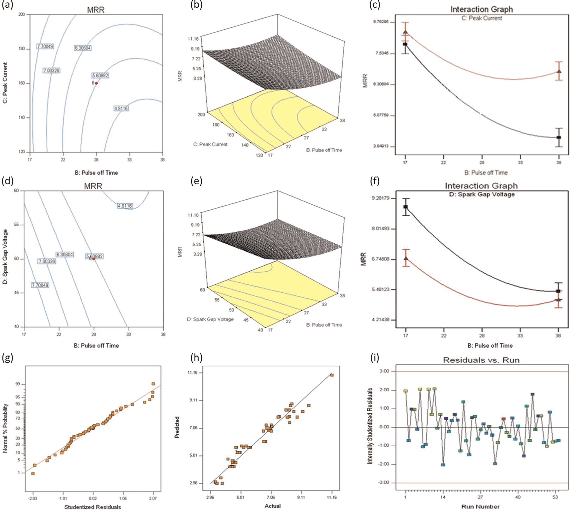
Response surface plot for MRR: (a) contour plot; (b and c) interaction plot at pulse on time = 0.9 µs, spark gap voltage = 50 V, wire feed = 7 m/min and wire tension = 950 g; (d) contour plot; (e and f) interaction plot at pulse on time = 0.9 µs, peak current = 160 A, wire feed = 7 m/min and wire tension = 950 g; (g) normal probability plot residuals; (h) actual versus predicted values and (i) residuals versus run.
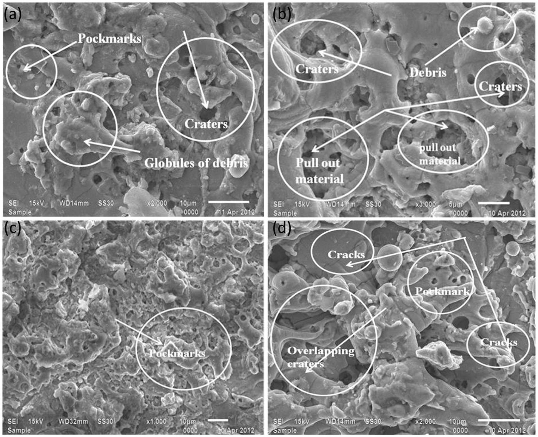
SEM micrographs (1000×, 2000×, 3000×): (a) Exp. No. 1, at Ton = 1.1 µs, Toff = 28 µs, Ip = 200 A, SV = 50 V, WF = 7 m/min, WT = 500 g; (b) Exp. No. 35, at Ton = 1.1 µs, Toff = 17 µs, Ip = 160 A, SV = 40 V, WF = 7 m/min, WT = 950 g; (c) Exp. No. 15, at Ton = 0.7 µs, Toff = 28 µs, Ip = 120 A, SV = 50 V, WF = 7 m/min, WT = 500 g and (d) Exp. No. 6, at Ton = 1.1 µs, Toff = 28 µs, Ip = 160 A, SV = 40 V, WF = 4 m/min, WT = 950 g.
SEM micrographs (1000×, 2000×, 3000×): (a) Exp. No. 1, at Ton = 1.1 µs, Toff = 28 µs, Ip = 200 A, SV = 50 V, WF = 7 m/min, WT = 500 g; (b) Exp. No. 52, at Ton = 1.1 µs, Toff = 28 µs, Ip = 200 A, SV = 50 V, WF = 7 m/min, WT = 1400 g; (c) Exp. No. 50, at Ton = 1.1 µs, Toff = 17 µs, Ip = 160 A, SV = 60 V, WF = 7 m/min, WT = 950 g and (d) Exp. No. 36, at Ton = 0.9 µs, Toff = 17 µs, Ip = 200 A, SV = 50 V, WF = 10 m/min, WT = 950 g.
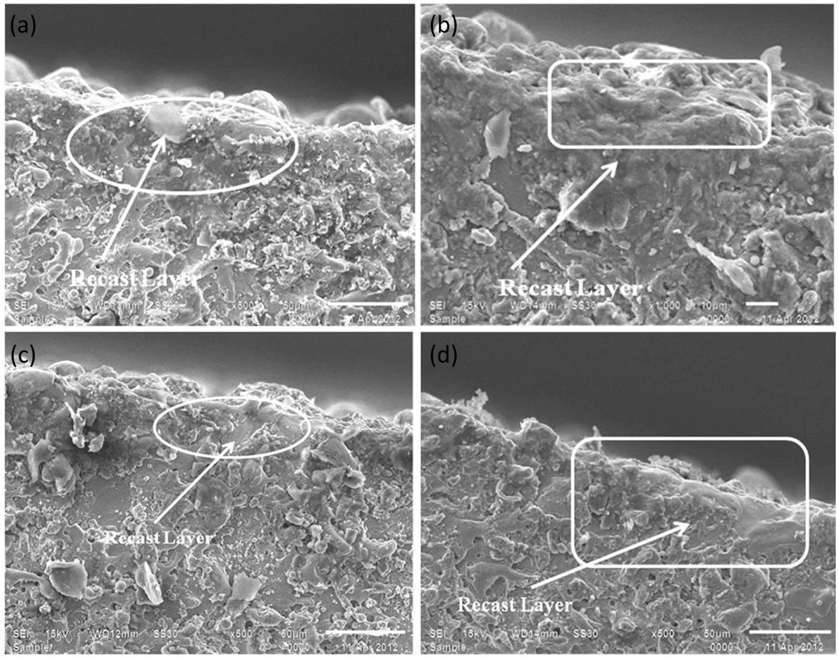
SEM micrograps of recast layer at various pulse on time and peak current: (a) Ton = 1.1 µs, Ip = 160 A; (b) Ton = 1.1 µs, Ip = 200 A; (c) Ton = 0.9 µs, Ip = 120 A and (d) Ton = 0.9 µs, Ip = 160 A.
Effect of process parameters on WWR
The term WWR is defined as loss of wire weight after machining. The WWR is calculated by using the following method

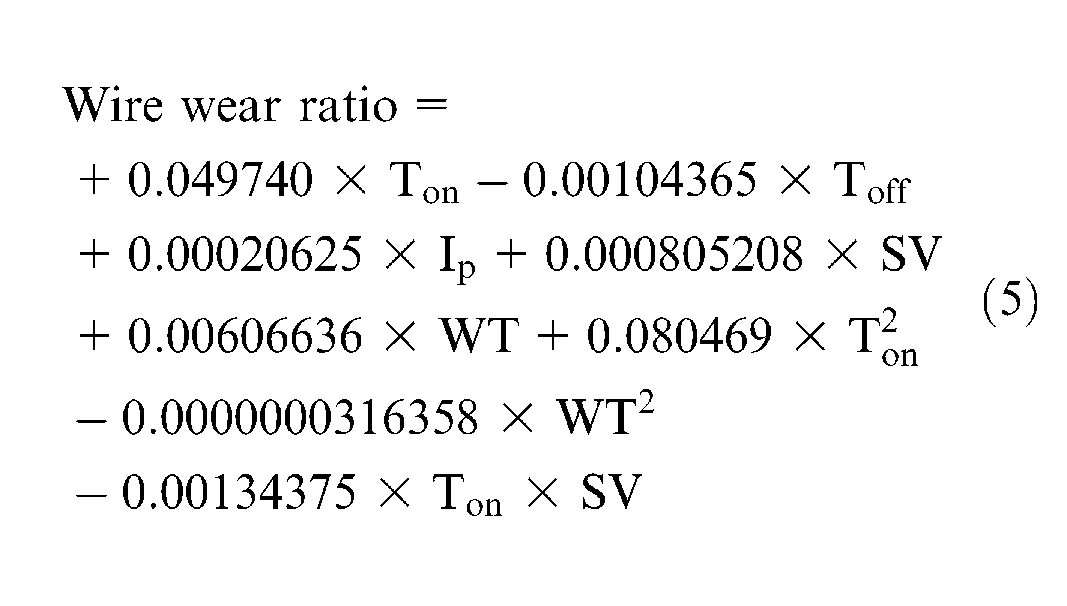
where ωR = WWR, ωL = wire wear loss, ωi = initial wire weight/unit length. The precision (Make SHIMADZU, Japan and model no. AUX220) balance with 0.001 g accuracy was used for the weight measurements. The average of three repeated measurements was taken to minimize the impact of measurement error. The initial wire was weighted as 6.293 g for its 25 m length. At the end of each experiment, the 25 m length of used wire is weighted and the loss of the weight was calculated. The loss of wire weight is due to the erosion and crater formed on the surface of wire. The regression equation for the WWR was modeled as follows
Based on analysis of variance (ANOVA) as shown in Table 5, A, B, C, D and one interaction (pulse on time SV) are found to be the significant parameters at 95% level. The model F value of 30.30 implies that the model is significant. There is only a 0.01% chance that “model F value” could occur due to noise. Values of “Prob > F” less than 0.05 indicate that model terms are significant. In this case, A, B, C, D, A2, F2 and AD are significant model terms. The “lack of fit F value” of 0.50 implies the lack of fit is not significant relative to the pure error. There is an 89.89% chance that such a large “lack of fit F value” could occur due to noise. The “Pred. R2” of 0.7755 is in reasonable agreement with the “Adj. R2” of 0.8156. “Adeq. Precision” measures the signal-to-noise ratio. The ratio of 21.504 indicates an adequate signal. It was observed from Figure 6(a)–(c) that when Ton and SV were set at the low level, 0.7 µs and 60 V, respectively, WWR is at the minimum value of 0.074, compared to other settings. Meanwhile, if the SV is fixed at 40 V and Ton is increased from 0.7 to 1.1 µs, the WWR was increased dramatically from 0.077 to 0.093. Based on the graph, it was the highest increment of WWR. Furthermore, when SV is set up at the high level (SV = 60 V) and Ton is set at 1.1 µs, the value of WWR was recorded to be 0.093. The WWR values obtained from both conditions are 0.074 and 0.093. From these results, the optimum setting parameters can be adjusted accordingly in order to minimize the WWR, as pulse on time at 0.7 µs and SV at 60 V. In addition to this, the normal plot of residuals data is normally distributed. It was experiential from Figure 6(d)–(f) that all the experimental results are in the region very near to the predicted values. It was observed experimentally that the increasing of pulse on time means more number of sparks on the surface of wire electrode, creating more number of craters on the wire and wire electrode wears out more rapidly. The WWR is always accompanied by high peak current and low pulse off time. 7
The analysis of variance for main and interaction effects of parameters on wire wear ratio.
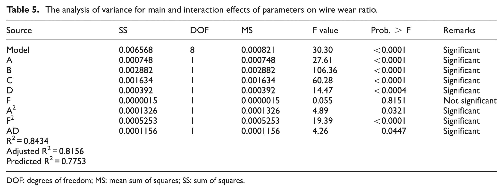
DOF: degrees of freedom; MS: mean sum of squares; SS: sum of squares.
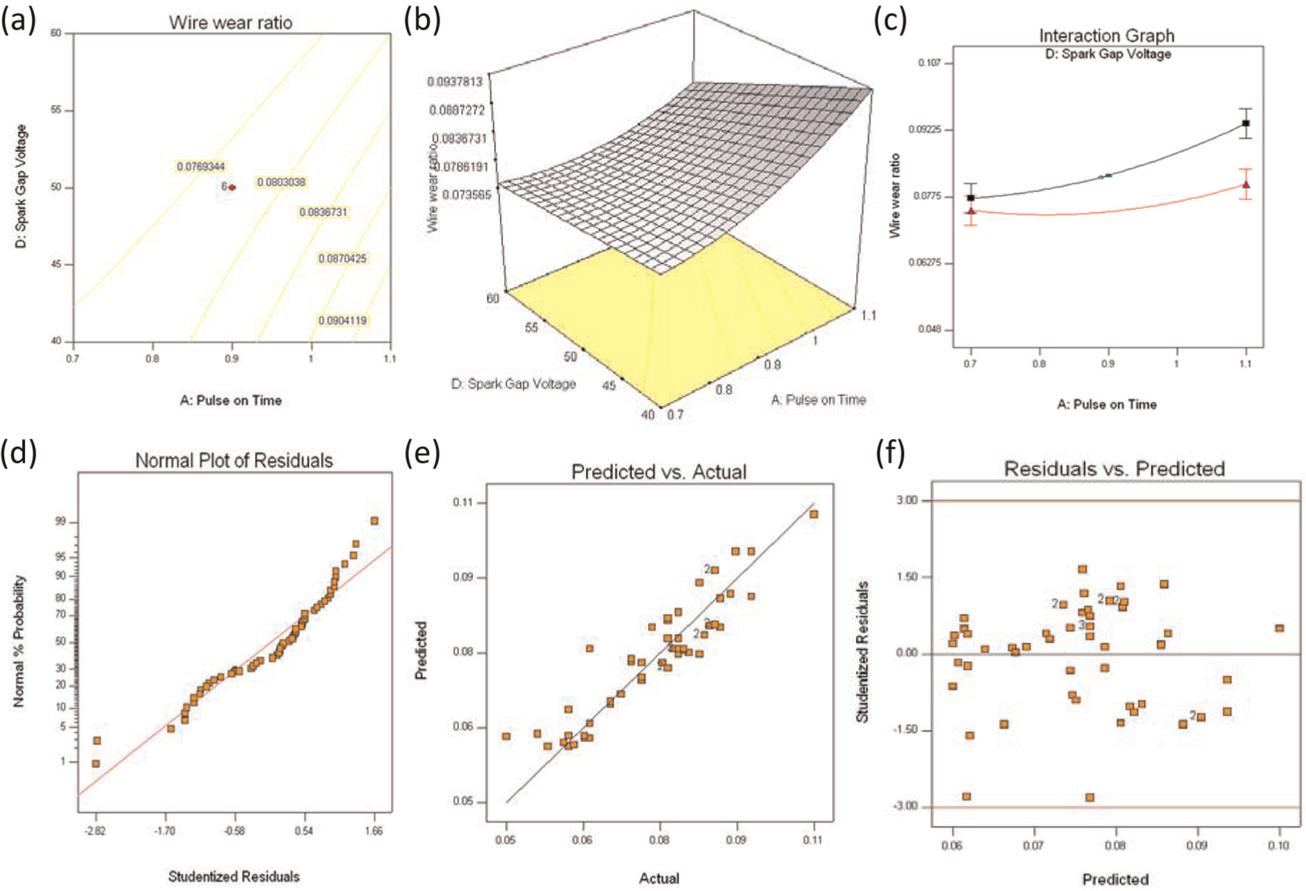
Response surface plot for wire wear ratio (WWR): (a) contour plot; (b and c) interaction plot at pulse off time = 28 µs, peak current = 160 A, wire feed = 7 m/min, wire tension = 950 g; (d) normal probability plot residuals; (e) actual versus predicted values and (f) residuals versus predicted.
Effect of process parameters on the surface roughness
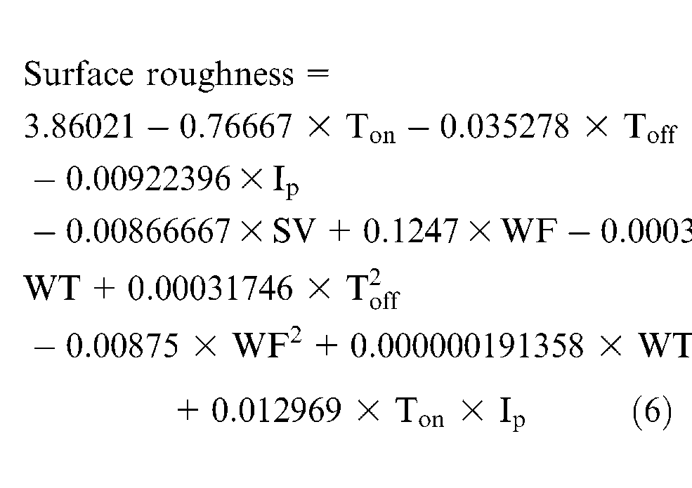
Surface roughness is an important process criterion, which dictates the condition of the surface component that has to be machined. If the surface finish of the machined work material is the decisive factor due to its application requirements, then the work material must be machined with low MRR. The quadratic model for surface roughness is represented as follows
Based on ANOVA as shown in Table 6, Ton, Toff, Ip, SV and one interaction (Ton × Ip) are significant to surface roughness. The P value for lack of fit is 0.1173, suggesting that this model adequately fits the data. The “Pred. R2” of 0.9527 is in reasonable agreement with the “Adj. R2” of 0.9646. It was observed from Figure 7(a)–(c) that the surface roughness is affected by interaction between pulse on time and peak current with value of 2.41–2.72 µm. When pulse on time was increased from 0.7 to 1.1 µs with peak current of 200 A, the surface roughness increased from 2.40 to 3.13 µm. It was observed from Figure 7(d)–(f) that all the experimental results are in the region very near to the predicted values, and hence, the developed model can be effectively used to predict the surface roughness in WEDM of pure titanium. At higher pulse on time and peak current, the discharge energy per pulse increases, which produces the deeper and wider overlapping craters, pockmarks, globules of debris and microcracks on the machined samples as seen in SEM micrographs (Figures 3 and 4). The rapid cooling and heating effects generate gas bubbles that explode when the discharge ceases. It is clear from Figure 4(d) that the diameter and depth of crater were deeper and wider due to high peak current (200 A) and low pulse off time (17 µs), which subsequently resulted in a large value of surface roughness (2.98 µm). At higher peak current, the impact of discharge energy on the surface of workpiece becomes greater, and thus, resulting erosion leads to the increase in deterioration of surface roughness.22,28 It was observed from Figure 4(c) that some titanium particle protruding and completely dislodged from the surface, which may happen at higher pulse on time (1.1 µs) and peak current (200 A).
The analysis of variance for main and interaction effects of parameters on surface roughness.
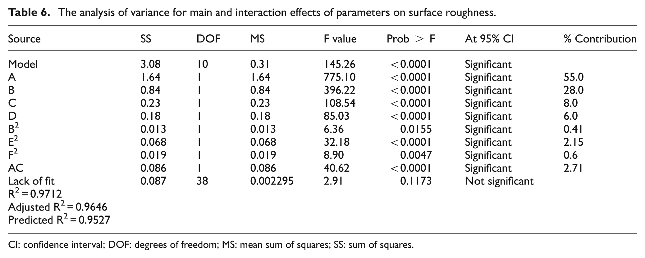
CI: confidence interval; DOF: degrees of freedom; MS: mean sum of squares; SS: sum of squares.
Contour and response surface plot for surface roughness: (a) contour plot; (b and c) interaction plot at pulse off time = 28 µs, spark gap voltage = 50 V, wire feed = 7 m/min and wire tension = 950 g; (d) normal probability plot residuals; (e) actual versus predicted values and (f) residuals versus run.
Crack formation
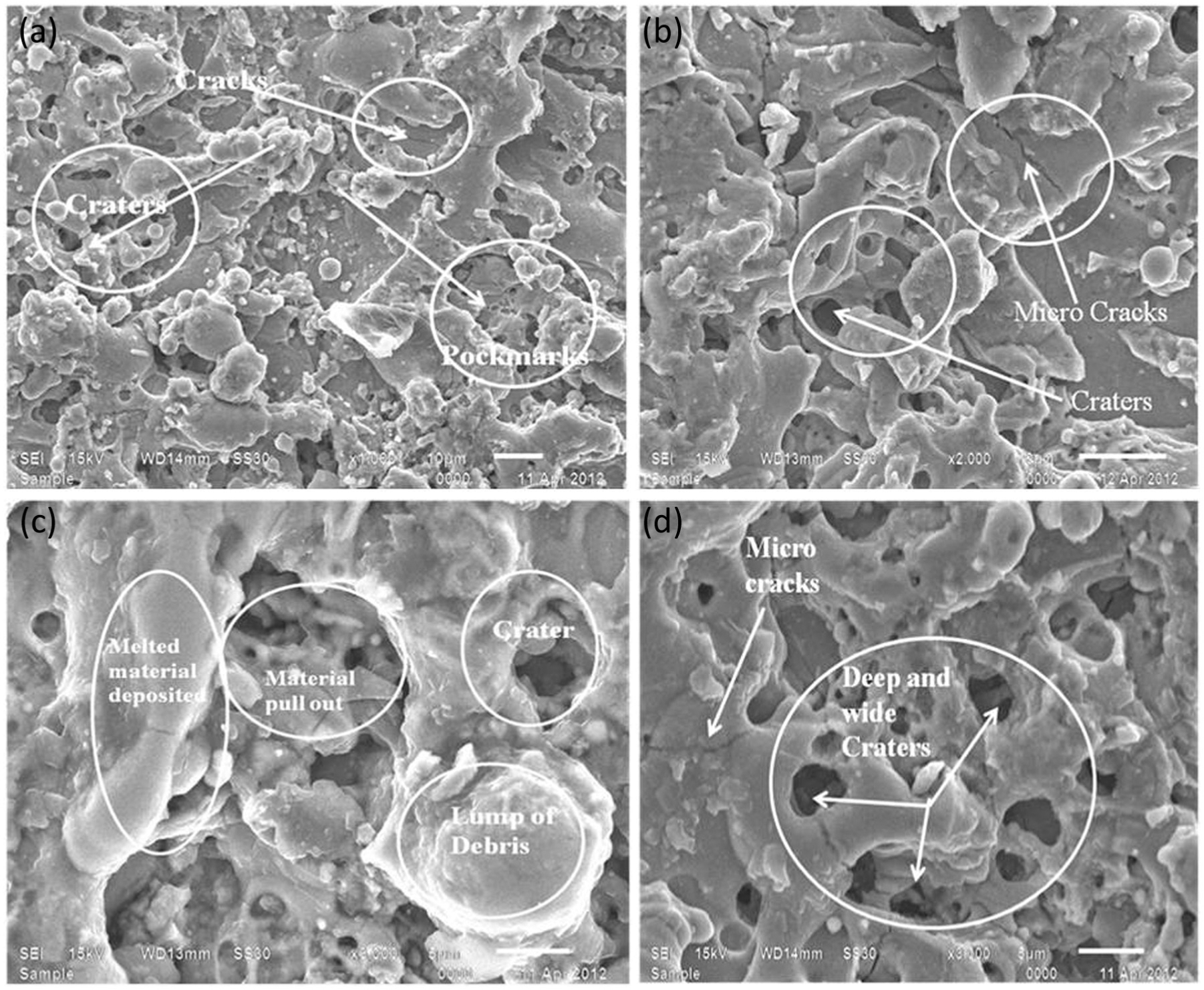
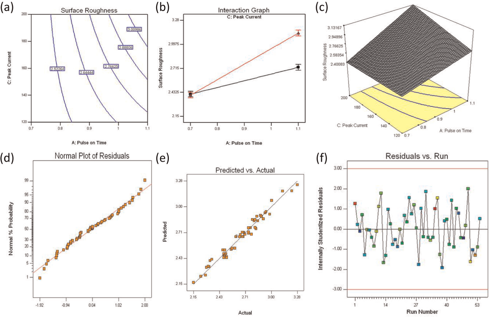
Based on the previous research work done by Lee and Li, 26 crack formation was usually associated with the development of high thermal stresses exceeding the fracture strength, as well as with plastic deformation. In addition, the formation of microcracks is not only influenced by the setting of machining parameters but also depended on several material properties such as tensile strength, thermal conductivity, thermal expansion coefficient and Young’s modulus. The subsurface cracks of WEDM machined samples indicate that the material is amorphous either in free form and/or in compound form. The formation of microcracks is generally accompanied by rapid cooling and heating by dielectric fluid. The heating and cooling process increases the yield stress, and the material plastically deformed during heating builds up the tensile stresses, which leads to crack formation. The crack distribution on the surface could be observed by evaluating the crack density and mean free path of the cracks.27xref ref-type="bibr" rid="bibr29-0954405413479791"/>-30 The surface crack densities at various peak current and pulse on time are observed in Figure 8(a)–(d). It is observed from these figures that the cracks were developed due to high pulse on time and peak current. The increase of pulse on time and peak current leads to intense heat conditions on the workpiece causing surface cracks developed in the material. Overall, the results show that the surface cracks were developed by increasing pulse on time and peak current.
SEM micrograps of subsurface cracks at various pulse on time and peak current: (a) Ton = 1.1 µs, Ip = 160 A; (b) Ton = 1.1 µs, Ip = 200 A; (c) Ton = 0.9 µs, Ip = 120 A and (d) Ton = 0.9 µs, Ip = 160 A.
Analyzing the wire rupture and wire wear topography
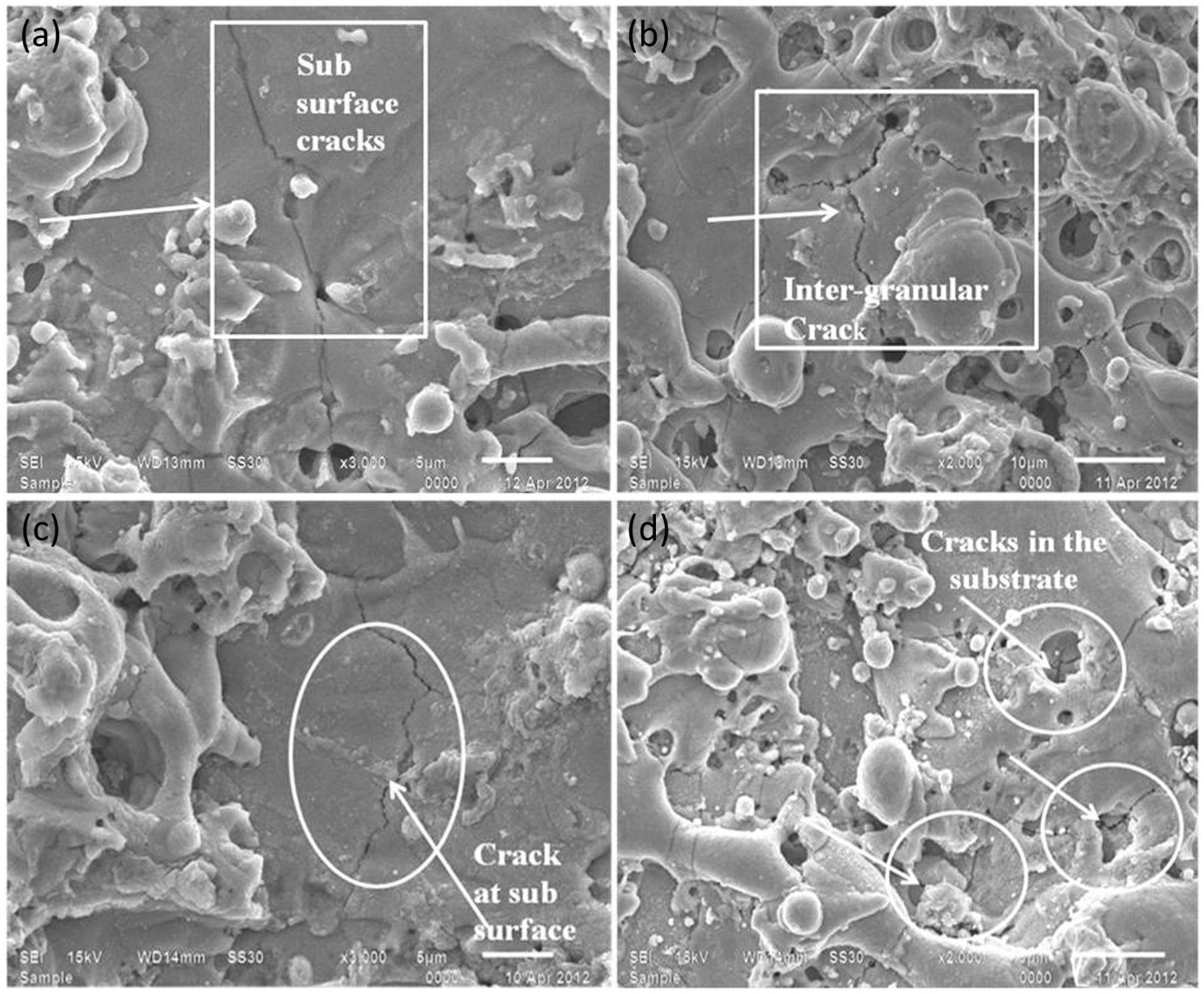
In WEDM, the cutting is done by brass wire having tensile strength of 900 N/mm2. The occurrence of wire rupture would result in a great increase of machining rate, decrease of machining accuracy and the deterioration of quality of machined surface. Due to the thermal effects that develop at the interface zone between the tool and workpiece, lot of material changes take place on the surface of the tool and workpiece. 31 In this regard, the material transfer characteristic of machined wire was investigated. The wire is fed through guide rolls causing abrasive action between wire and workpiece. This may result in reduced cross section, and also the surface characteristics of the workpiece may get affected. Hence, proper care should be taken in loading the spool to the machine to avoid wire deflection and breakage. In this study, two types of wire rupture were observed: one is due to high peak current and other is increased spark frequency. Figure 9(a)–(e) shows the micrograph of worn out wire. A large number of different craters and residuals of debris adhered to the surface of wire electrode were observed by energy-dispersive X-ray (EDX), as shown in Figure 9(f). The residuals of copper, carbon, oxygen and Ti were detected in wire electrode. This may be due to the melting and resolidification of the titanium and brass wire electrode after WEDM. Increasing the peak current leads to generation of higher discharge energy in the spark gap, which may result in the increase in the wire wear rate and wire breakage.24,25 When the debris in the gap cannot be flushed properly by dielectric, it may result in the arcing and wire breakage occurs. In addition, since the spark gap is too narrow, a portion of discharging energy was absorbed by wire electrode. Hence, the surface of wire melts due to the induced high temperature.
SEM micrographs (250× and 500×) of the machined wire electrode surface for machining of pure titanium at (a) fresh wire; (b) Exp. No. 1, at Ton = 1.1 µs, Toff = 28 µs, Ip = 200 A, SV = 50 V, WF = 7 m/min, WT = 500 g; (c) Exp. No. 35, at Ton = 1.1 µs, Toff = 17 µs, Ip = 160 A, SV = 40 V, WF = 7 m/min, WT = 950 g; (d and e) Exp. No. 15, at Ton = 0.7 µs, Toff = 28 µs, Ip = 120 A, SV = 50 V, WF = 7 m/min, WT = 500 g and (f) EDX of machined wire electrode at Ton = 0.9 µs, Toff = 38 µs, Ip = 160 A, SV = 50 V, WF = 4 m/min, WT = 500 g.
EDX and X-ray diffraction analysis
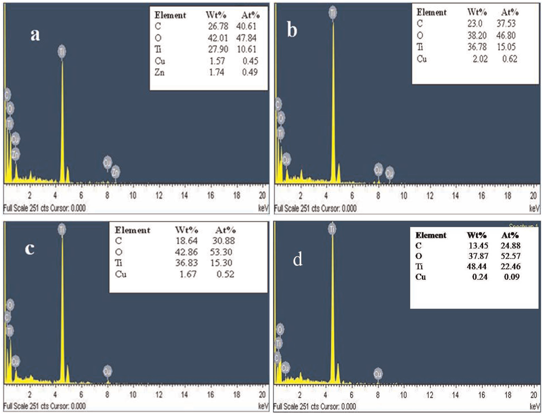
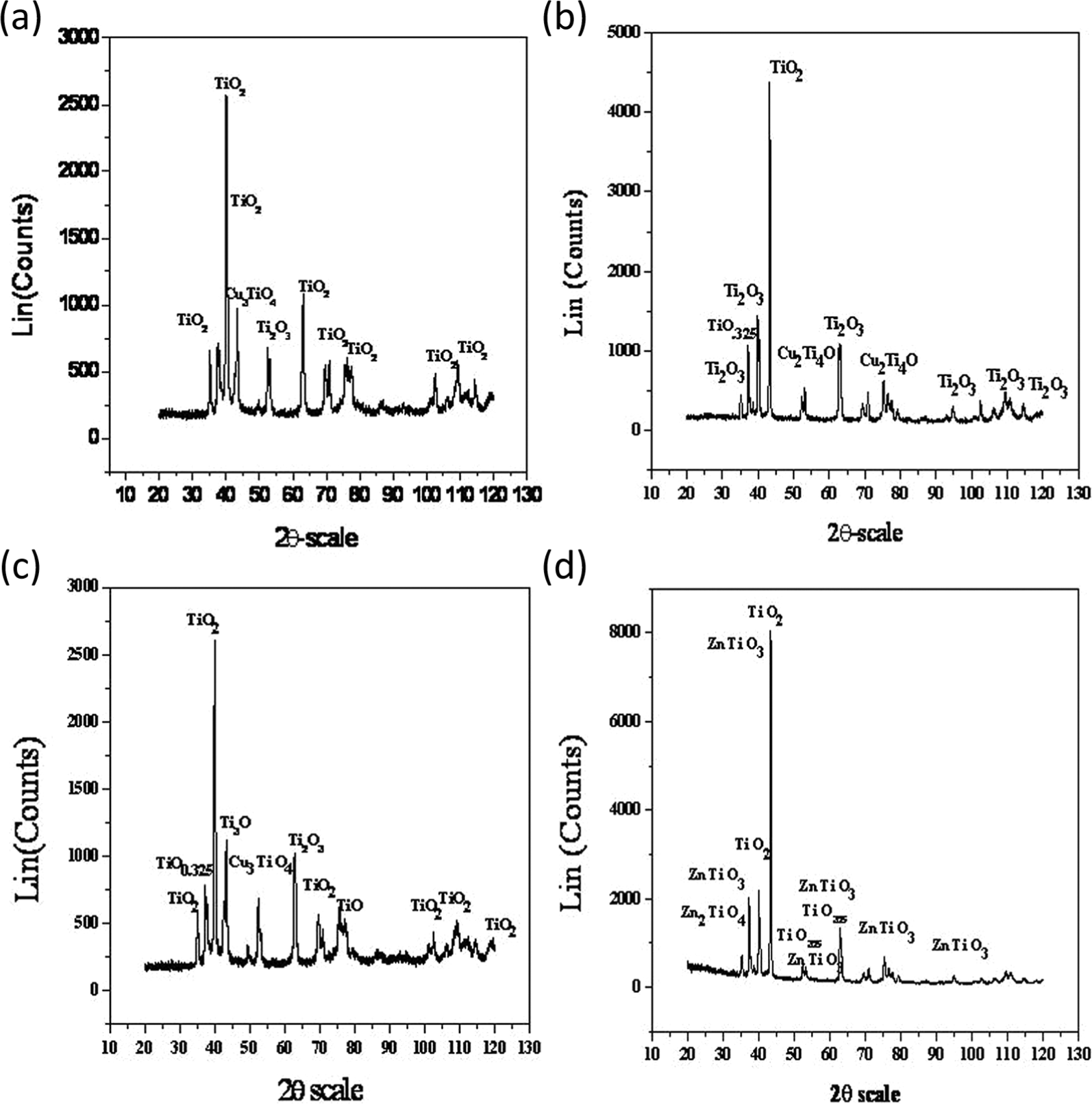
The compositions of samples were detected through EDX. EDX analysis is the technique that is used to identify the elemental composition of the machined samples. The output of an EDX analysis is a plot of how frequently an X-ray is received for each energy level. An EDX spectrum normally displays peaks corresponding to the energy levels for which the most X-rays had been received. Each of these peaks is unique to an atom and therefore corresponds to a single element. The higher a peak in a spectrum, the more concentrated the element in the specimen. 32 Figure 10 shows the EDX of affected surfaces, which are obtained by accelerating voltage of 3 kV. Through EDX analysis, the residuals of copper and zinc were also detected in the machined samples. This may be due to the melting, evaporation and resolidification of the brass wire electrode transferred to the work material. The presence of oxygen in the titanium probably was due to oxidation as a result of high temperature involved in the process. Although EDX result showed that carbon and oxygen (O) also existed in the titanium, these elements were observed due to the fact that dielectric fluid with debris normally contains carbon and oxygen. Furthermore, the X-ray diffraction (XRD) pattern analysis confirms the migration of tool elements (anode); dielectric fluid elements were migrated to the work surface and they formed different compounds like titanium dioxide (rutile) (TiO2), (TiO0.325), TiO, Ti2O3, ilmenite (Fe2Ti4O) and copper titanium dioxide (Cu3TiO4). The phases were identified in the form of peaks at 2θ scale. The plots of identified phases were shown in Table 7 and Figure 12. The XRD peaks of compounds like titanium dioxide, copper titanium oxide and zinc titanium oxide were observed in Figure 11. During melting and resolidification of pure titanium, the phase is transferred from α to β, which formed the hexagonal crystal structure. The solubility of Fe with titanium formed the martensitic structure that is very hard, brittle and amorphous. 23 The amorphous structure develops the cracks due to rapid cooling. These results were observed in SEM micrographs (Figure 8).
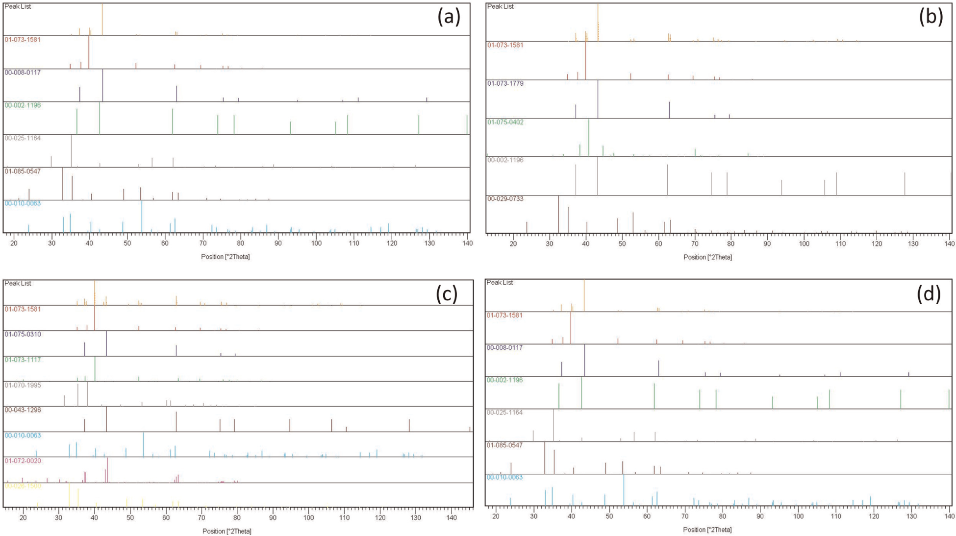
XRD plot of identified phases.
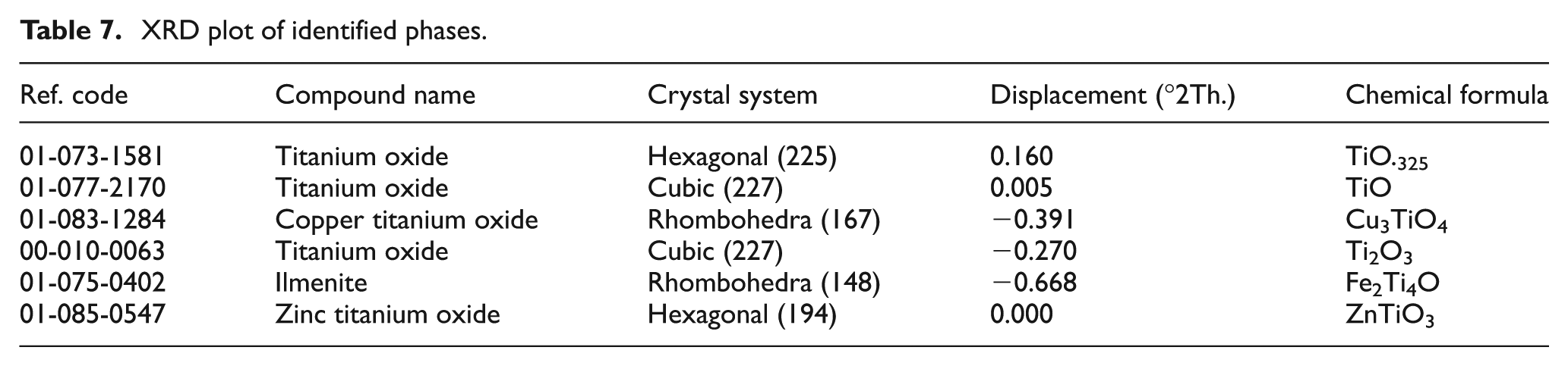
EDX analysis of pure titanuim after WEDM for (a) Exp. No. 1, (b) Exp. No. 35, (c) Exp. No. 15 and (d) Exp. No. 6.
XRD pattern of the machined surface: (a) Exp. No. 1, at Ton = 1.1 µs, Toff = 28 µs, Ip = 200 A, SV = 50 V, WF = 7 m/min, WT = 500 g; (b) Exp. No. 15, at Ton = 0.7 µs, Toff = 28 µs, Ip = 120 A, SV = 50 V, WF = 7 m/min, WT = 500 g; (c) Exp. No. 6, at Ton = 1.1 µs, Toff = 28 µs, Ip = 160 A, SV = 40 V, WF = 4 m/min, WT = 950 g and (d) Exp. No. 35, at Ton = 1.1 µs, Toff = 17 µs, Ip = 160 A, SV = 40 V, WF = 7 m/min, WT = 950 g.
XRD phase plots of the machined surface: (a) Exp. No. 1, at Ton = 1.1 µs, Toff = 28 µs, Ip = 200 A, SV = 50 V, WF = 7 m/min, WT = 500 g; (b) Exp. No. 15, at Ton = 0.7 µs, Toff = 28 µs, Ip = 120 A, SV = 50 V, WF = 7 m/min, WT = 500 g; (c) Exp. No. 6, at Ton = 1.1 µs, Toff = 28 µs, Ip = 160 A, SV = 40 V, WF = 4 m/min, WT = 950 g and (d) Exp. No. 35, at Ton = 1.1 µs, Toff = 17 µs, Ip = 160 A, SV = 40 V, WF = 7 m/min, WT = 950 g.
Multi-response optimization based on desirability
The desirability function can be used to combine multiple responses into one response called the “desirability function” by choice of value from 0 (one or more product characteristics are unacceptable) to 1 (all product characteristics are on target). The method is attractive because it is intuitive and simple. The inputs are mean response estimates, target value and upper and lower acceptability bounds. The individual desirability is combined using the geometric mean. The desirability of a product characteristic value depends on the lower and upper ranges of product specification. Improper selection of ranges can result in a very different “optimum.” The basic idea of the desirability function approach is to transform a multiple response problem into a single response problem by means of mathematical transformations. The desirability function involves transformation of each estimated response variable
Step 1
Calculate the individual desirability (di) for each response (
Step 2
Combine individual desirabilities to obtain composite desirability (DG) for given weights of MRR, WWR and surface roughness. Composite desirability is the weighted geometric mean of individual desirability for the given responses.
Step 3
Maximize the composite desirability and identify the optimal parameter combinations
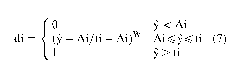
If the target (ti) is to minimize a response, the individual desirability (di) is calculated as
where Ai = lower limit value of response
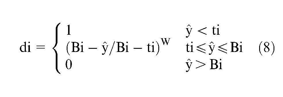
If the object for the response is a target value, then individual desirability (di) is calculated as
If the importance is same for each response, the composite desirability (DG), the geometric mean of all desirability functions, is given by
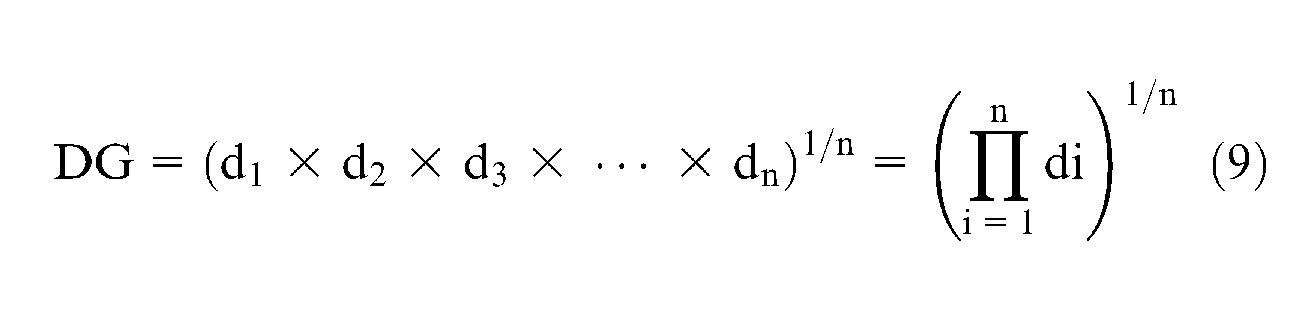
where n = number of responses = 3.
It can be extensive to reflect the possible difference in the importance of different responses by giving weights. Where the weight wi satisfies 0 < wi < 1 and
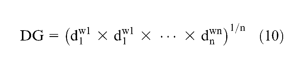
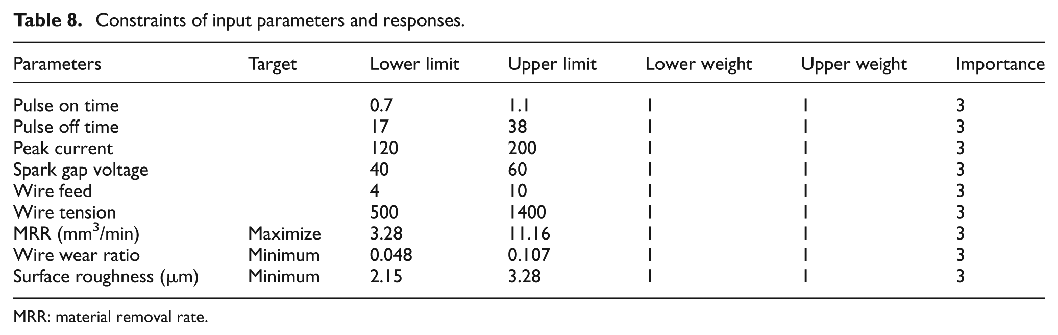
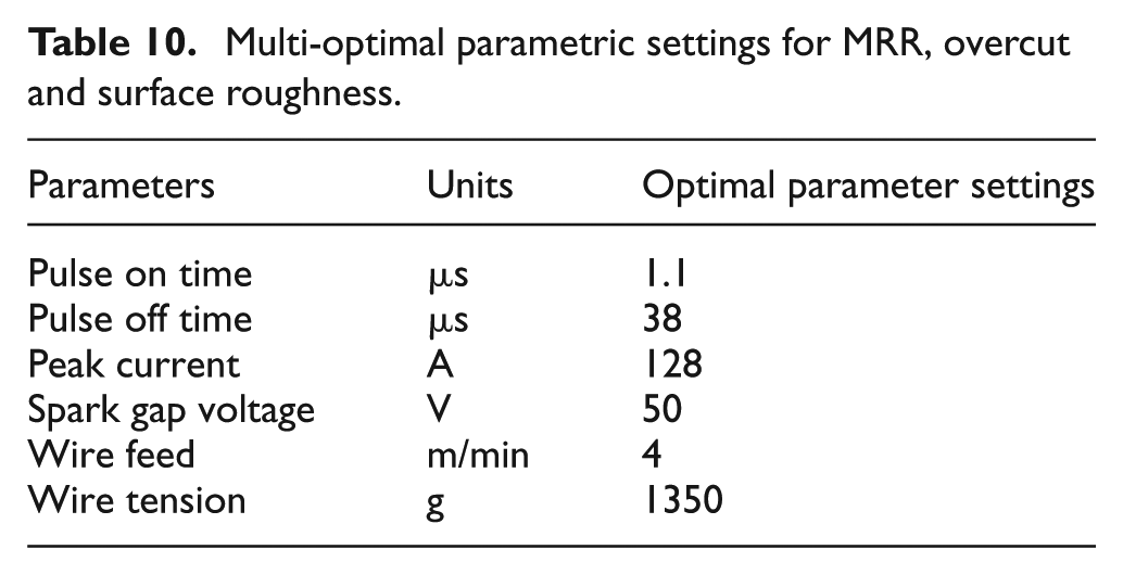
Table 8 shows the constraints of input parameters and that of responses and the goal and weights assigned to each parameter. Table 9 shows the values of 25 levels of combinations of process parameters that will give a high value of composite desirability (ranged from 0.603 to 0.527), and the predicted values of responses obtained are also given. The value of composite desirability (D) was taken as 0.603. Table 10 gives the optimal input process parametric setting for multi-response optimization. The current optimal process parameter setting is Ton of 1.1 µs, Toff of 38 µs, Ip of 128 A, SV of 50 V, WF of 4 m/min and WT of 1350 g. To show the sensitivity of the results, contour plots for overall desirability and optimized histograms of the three responses (MRR, WWR and surface roughness) are shown in Figure 13(a) and (b). The near-optimal region was located close to the right-hand center region of the plot, which had a composite desirability value greater than 0.603 that gradually reduced as we moved left and upward.
Constraints of input parameters and responses.
MRR: material removal rate.
Process parameter combinations for high value of desirability.
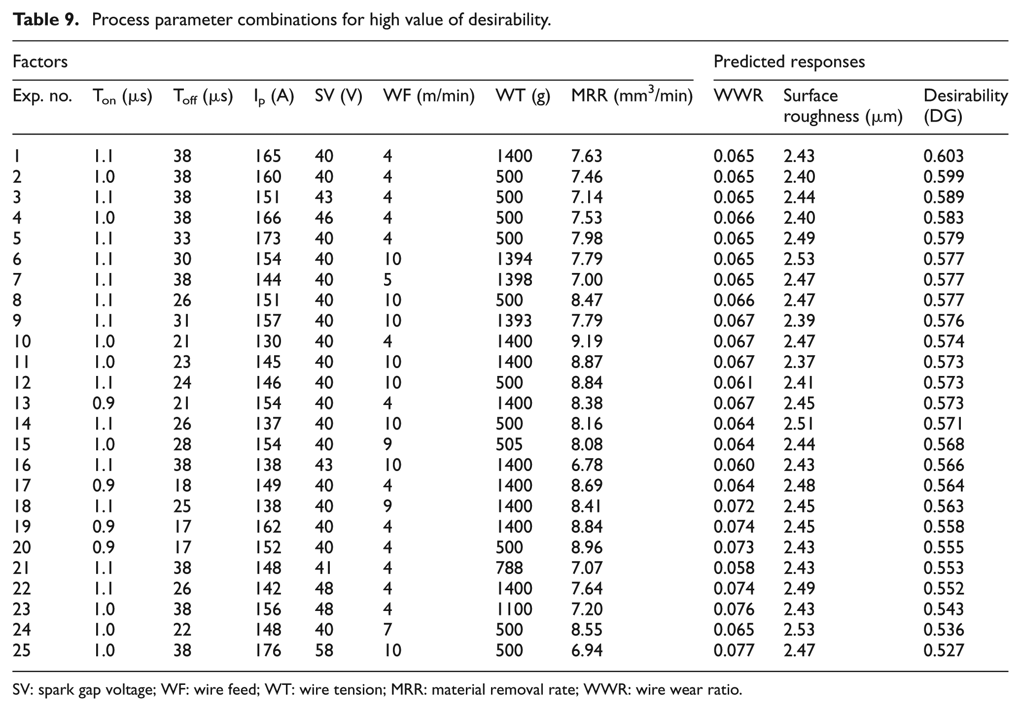
SV: spark gap voltage; WF: wire feed; WT: wire tension; MRR: material removal rate; WWR: wire wear ratio.
Multi-optimal parametric settings for MRR, overcut and surface roughness.
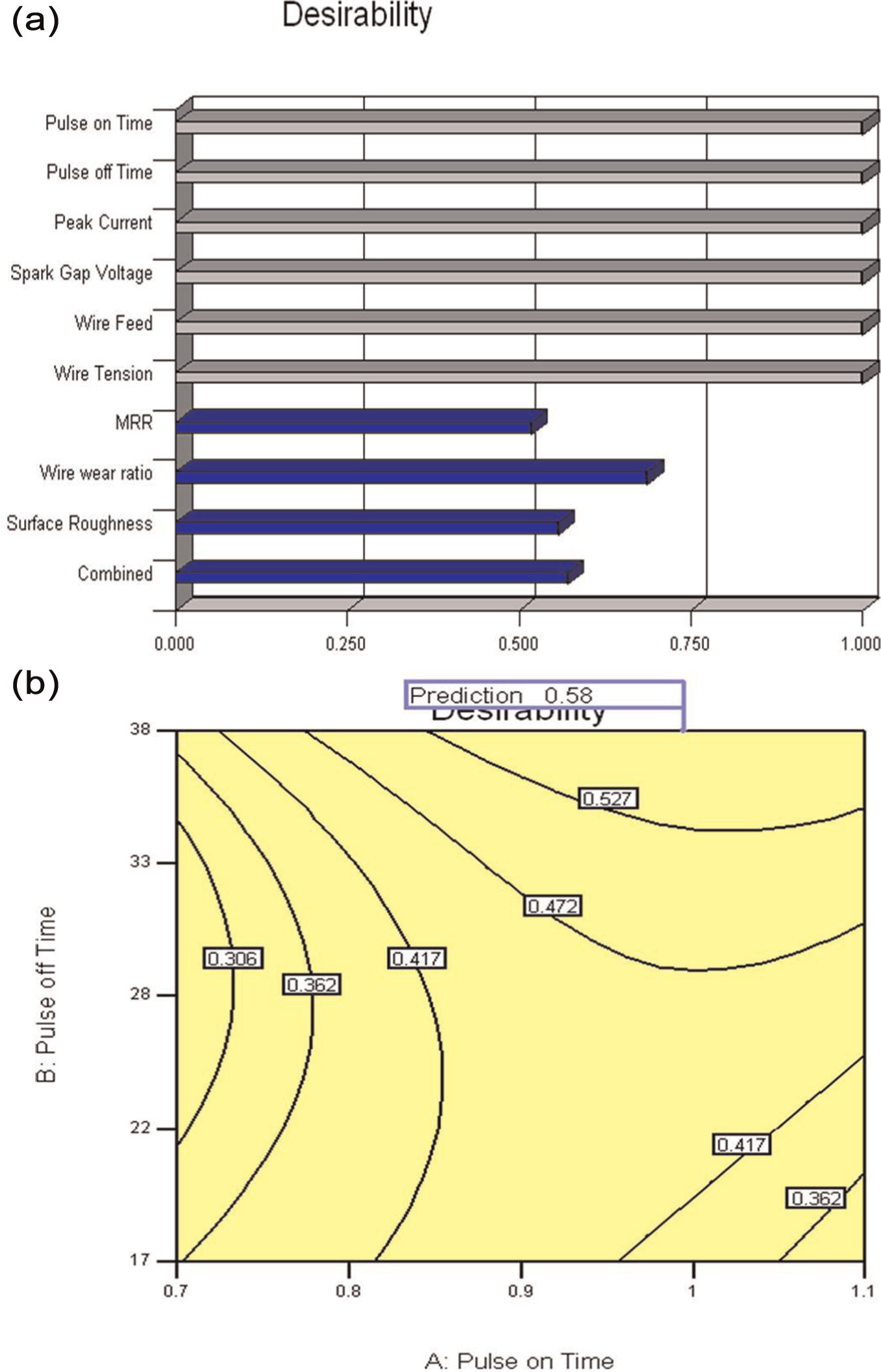
(a) Bar histograms and (b) contour plot for results of overall desirability functions (at peak current = 200 A, SV = 60 V, WF = 4 m/min, WT = 500 g).
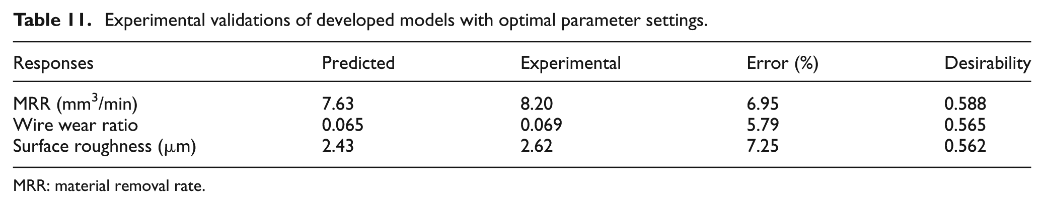
Confirmation experiment
The confirmatory experiments were performed to validate the optimal input parametric setting for MRR, WWR and surface roughness. The observed experimental results for performance measures are 8.20 mm3/min, 0.069 and 2.43 µm, respectively. Table 11 shows the error percentage for experimental validation of the developed models for the responses with optimal parametric setting. From the analysis, it was concluded that the error between experimental and predicted values for MRR, WWR and surface roughness lies within 6.95%, 5.79% and 7.25%, respectively. Obviously, this confirms excellent reproducibility of the experimental conclusions.
Experimental validations of developed models with optimal parameter settings.
MRR: material removal rate.
Conclusion
In this experimental work, the MRR, WWR and surface roughness in WEDM of pure titanium were modeled and analyzed using response surface methodology. The following conclusions were drawn:
The residuals of copper, carbon and zinc were detected in the machined samples using EDX analysis. This could be attributed to the migration of tool and dielectric fluid elements (after decomposition) to the work surface. The presence of oxygen in the titanium probably was due to oxidation as a result of high temperature involved in the process.
The XRD pattern analysis confirmed the migration of tool elements (anode), dielectric fluid elements to the work surface, and furthermore, the elements formed different compounds such as titanium dioxide (rutile) (TiO2), (TiO0.325), TiO, Ti2O3, Ilmenite (Fe2Ti4O) and copper titanium dioxide (Cu3TiO4).
The investigation of surface crack densities at different values of peak current and pulse on time revealed that the peak values of these parameters produced intense heat conditions in the machining zone (followed by rapid cooling) that yielded higher crack densities. The solidified material was observed as amorphous either in free form or in compound form due to melting and vaporization.
Wire rupturing was observed at higher values of peak current and spark frequency. The wire electrode surface exhibited formation of craters and the residuals of copper, carbon, oxygen and Ti debris adhered to it, as observed from EDX analysis. This was concluded to be due to the melting and resolidification of the titanium and brass wire electrode after WEDM.
During melting and resolidification of pure titanium, the phase was transferred from α to β which formed the hexagonal crystal structure. The solubility of Fe with titanium formed the martensitic structure, which in amorphous form developed cracks under conditions of rapid cooling.
From the examination of surface texture, it was concluded that during WEDM of titanium, molten material is deposited in the form of globules of debris. A significant variation in the crater size was also observed that could be related to the uneven distribution of discharge energy along the surface.
The existence of recast layer was confirmed through the SEM of machined work surface. However, the extent (thickness) of recast layer was observed to be much less than other processes such as die sinking EDM.
The crater size was larger (while machining Ti) along with a higher frequency of the globules of debris on the machined surface than that observed in the WEDM of other materials such as steel, as seen from the comparative analysis of the SEM images from this study and studies reported by other researchers. These effects may be attributed to the poor thermal conductivity of titanium, which restricts the fast dissipation of heat from machining zone, resulting in prolonged melting and vaporization of the material.
Pulse peak current and pulse on time were identified as the most significant factors for surface roughness and WWR. Peak values of these parameters resulted in higher surface roughness due to formation of wider and deeper, overlapping craters due to intense melting and vaporization of the substance sustained for a prolonged duration. After crossing a threshold value of peak current (200 A), wire breakage occurred in a repetitive fashion due to loss of process stability.
Footnotes
Appendix 1
Acknowledgements
The authors highly acknowledge central tool room (CTR), Ludhiana, Punjab, India, for providing the necessary experimental setup and other facilities during the research work.
Funding
This research received no specific grant from any funding agency in the public, commercial or not-for-profit sectors.