
Abstract
The search for efficient but inexpensive photovoltaics over the past decade has been disrupted by the advent of lead-halide perovskite solar cells. Despite impressive rises in performance, the toxicity and stability concerns of these materials have prompted a broad, interdisciplinary community across the world to search for lead-free and stable alternatives. A set of such materials that have recently gained attention are semiconductors in the CuI–AgI–BiI3 phase space and their derivatives. These materials include ternary silver bismuth iodide compounds (Ag a Bi b I a +3b), ternary copper bismuth iodide Cu–Bi–I compounds and quaternary Cu–Ag–Bi–I materials, as well as analogues with Sb substituted into the Bi site and Br into the I site. These compounds are comprised of a cubic close-packed sub-lattice of I, with Ag and Bi occupying octahedral holes, while Cu occupies tetrahedral holes. The octahedral motifs adopted by these compounds are either spinel, CdCl2-type, or NaVO2-type. NaVO2-type Ag a Bi b I a +3b compounds are also known as rudorffites. Many of these compounds have thus far demonstrated improved stability and reduced toxicity compared to halide perovskites, along with stable bandgaps in the 1.6–1.9 eV range, making them highly promising for energy harvesting and detection applications. This review begins by discussing the progress in the development of these semiconductors over the past few years, focusing on their optoelectronic properties and process–property–structure relationships. Next, we discuss the progress in developing Ag–Bi–I and Cu–Bi–I compounds for solar cells, indoor photovoltaics, photodetectors, radiation detectors and memristors. We conclude with a discussion of the critical fundamental questions that need to be addressed to push this area forward, and how the learnings from the wider metal-halide semiconductor field can inform future directions.
Keywords
Introduction
Metal-halide semiconductors have recently gained significant interest as novel energy conversion materials.1–3 This has been driven by the astonishing rises in performance of lead-halide perovskite (LHP) devices, originally in photovoltaics,4,5 but now also in light-emitting diodes, 6 radiation detectors, 7 field-effect transistors, 8 photoelectrochemical cells 9 and many other applications. However, lead is toxic and regulated in many jurisdictions, which, for example, may prevent the commercial use of LHP devices in consumer electronics.10,11 Furthermore, the polar solvents used for processing LHPs are toxic and environmentally harmful. 12 These limitations have prompted a global effort to develop alternative classes of materials that can replicate the exceptional optoelectronic properties of the LHPs (especially their defect tolerance),13,14 but which are stable (under thermal, environmental and light stressors) and overcome the toxicity challenges. However, simply substituting Pb for Sn or Ge has led to perovskites with inferior photovoltaic performance that still have limited stability. 15 In considering the broader family of metal-halide semiconductors, ternary and quaternary compounds within the CuI–AgI–BiI3 phase space have recently gained increasing attention.
Ternary Ag–Bi–I and Cu–Bi–I semiconductors were originally investigated several decades ago as potential ionic conductors, but were found to exhibit poor ionic conductivity.16–20 Following the rise in efforts to find lead-free alternatives to metal-halide perovskites, two groups reported the use of Ag–Bi–I compounds in photovoltaics in 2016, with a patent from Turkevych et al. 21 reporting 4.3% power conversion efficiency (PCE), and a paper from Kim et al. 22 reporting 1.22% PCE. Since then, there have been many efforts to develop these materials as solar cells, particularly since the optical limit in efficiency (i.e. spectroscopic limited maximum efficiency (SLME)) is well in excess of 20%, 23 showing there to be much room for improvement. In addition, these materials have been shown to have highly promising absorption properties for indoor light harvesting, with SLMEs exceeding 50%.23,24 In 2017, it was proposed to call these Ag–Bi–I compounds 'rudorffites' because the Ag-rich compounds adopted a NaVO2-type structure, which was first investigated by Rüdorff and Becker in 1954. 25 However, as will be discussed in the ‘Structure–property relationships of compounds in the CuI–AgI–BiI3 phase space, and their derivatives’ section, Ag–Bi–I semiconductors do not adopt only one structure, but also the layered CdCl2 structure and three-dimensional (3D) spinel structure. Although there is a tendency in the wider field now to collectively refer to the family of Ag–Bi–I compounds (and their substitutional derivatives) as rudorffites, we emphasise that this is not strictly correct, since ‘rudorffite’ would then also be referring to compounds that do not have the NaVO2 structure.
Beyond promising performance, the Ag–Bi–I compounds are advantageous in that they have stable performance in photovoltaic devices in ambient air,26,27 with structural and optoelectronic properties that are tunable through the composition (e.g. the ratio of Ag:Bi cations).20,24 There has also been rekindled interest in Cu–Bi–I compounds, but some of these materials have been reported to not be as stable as their ternary Ag-based analogues. 28 Including both Cu and Ag to form quaternary compounds has been found to retain the stability of Ag–Bi–I compounds, but also reduce the total quantity of Ag (which is expensive and toxic to aquatic life when released to water as Ag+). 28 However, these materials are at an early stage in their development, and there are many unresolved questions on their process–property–structure relationships, such as what trap states limit performance, and the role of carrier–phonon coupling on charge-carrier transport. Answering these questions will be crucial to moving the field forward towards the efficiency limits of these materials.
This Full Critical Review examines the potential and future directions of the family of materials within the CuI–AgI–BiI3 phase space, as well as their derivatives, for both solar and visible-light harvesting for optoelectronic applications, as well as more broadly for energy conversion and detection. The scope of this review is shown in Figure 1. While there have been many previous reviews on LHPs and pnictogen-based perovskite-inspired materials (PIMs; see, e.g. Cui et al., 33 Jin et al. 34 and Huang et al. 35 ), rudorffites and other Cu–Ag–Bi–I materials have not featured in these in detail. Given the gathering pace of this emerging field, a comprehensive review focused on these materials is called for, 36 especially to highlight important recent developments, including carrier localisation, the role of defects on photovoltaic performance, and advances in indoor light harvesting, which have not been covered in previous reviews. The review begins by discussing the structure–property relationships of Ag–Bi–I semiconductors (which have by far the largest body of literature), followed by Cu–Bi–I compounds, and then the quaternary Cu–Ag–Bi–I materials. Within each sub-section for each set of materials, we discuss the structure, optoelectronic properties, charge-carrier transport properties and the effects of chemical substitution on these properties. Furthermore, we discuss the stability of the materials as a whole. Each section also briefly covers the synthesis methods investigated for each set of materials, but our emphasis in this review is on the core principles, and we do not extensively summarise the various synthesis routes attempted, which can be found in other reviews.34,36 This discussion on structure–property relationships is then followed by a detailed discussion on the performance of these materials in solar cells (including how morphology can be controlled through processing), indoor photovoltaics (IPVs), radiation detectors and memristors. We also discuss the potential for applying these materials in photocatalysis and photoelectrochemistry. Finally, we discuss the key outstanding challenges and future directions for this field.
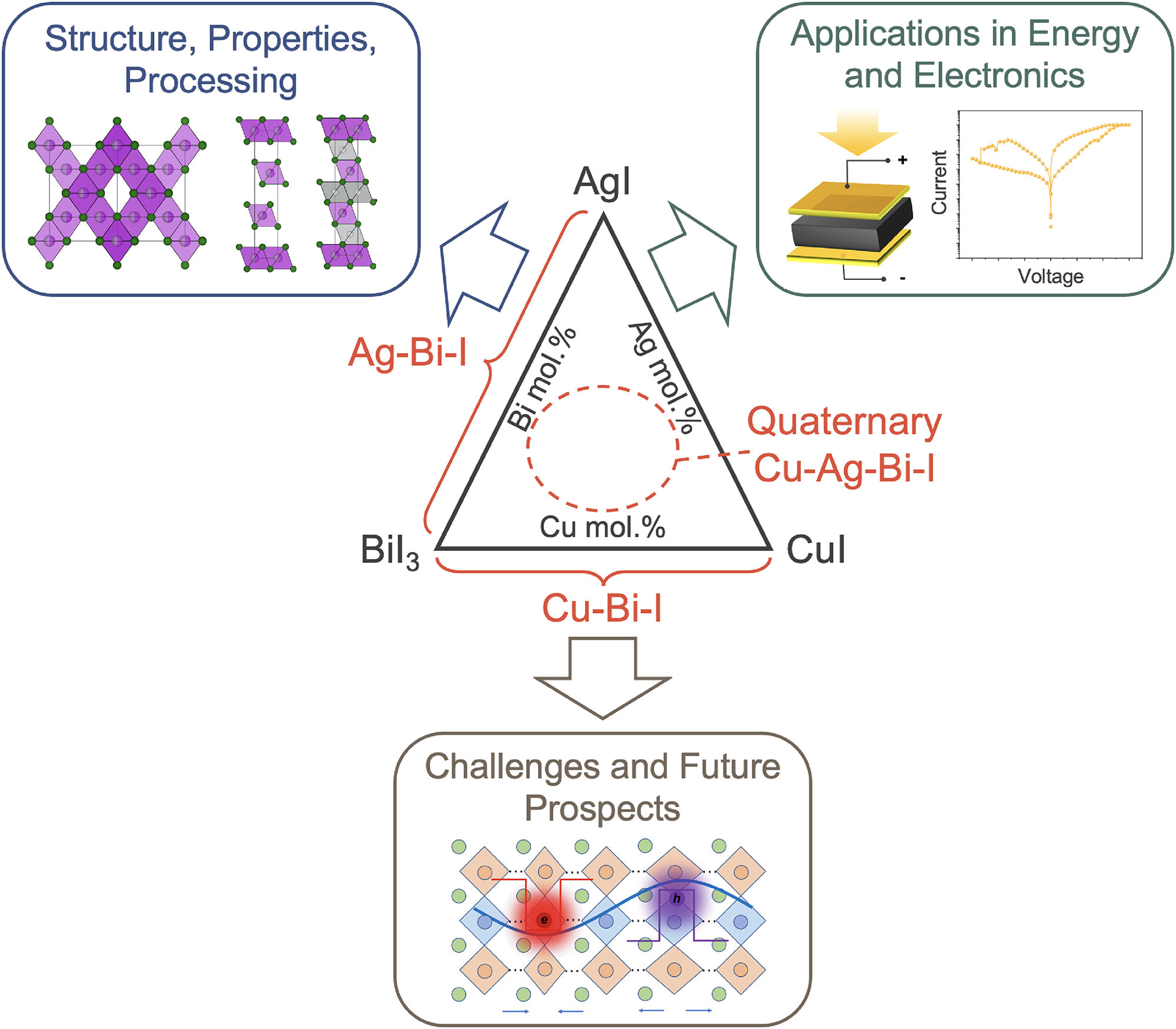
Overview and structure of this Full Critical Review. The materials focused on are ternary Ag–Bi–I and Cu–Bi–I semiconductors, along with quaternary Cu–Ag–Bi–I semiconductors and derivatives from compositional engineering. This review focuses on the crystal structure and properties, with a brief discussion of the processing, followed by the applications of these materials in energy and electronic devices (solar cells, IPVs, photodetectors, X-ray detectors and memristors). We conclude with a discussion of current challenges, open questions and future opportunities. Structures shown inset of the “Structure, Properties, Processing” box reproduced under the terms of the CC-BY license from Sansom et al. 29 Copyright 2021, The Authors. Figures included in the Applications box reproduced with permission from Tie et al. 30 (Copyright 2020, American Chemical Society) and Ye et al. 31 (Copyright 2022, Royal Society of Chemistry). In the Outlook box, the image was reproduced under the terms of the CC-BY-NC license from Wu et al. 32 Copyright 2021, The Authors.
Structure–property relationships of compounds in the CuI–AgI–BiI3 phase space, and their derivatives
Over the past five years, the subset within the CuI–AgI–BiI3 phase space of materials that have gained the greatest attention are the ternary Ag–Bi–I compounds. In particular, Ag3BiI6,37–39 Ag2BiI5,40–43 AgBiI444–46 and AgBi2I722,47–49 have been popular. We therefore begin this section by discussing these Ag–Bi–I compounds, before discussing Cu–Bi–I compounds, followed by the quaternary Cu–Ag–Bi–I compounds. Within each of these three sub-sections, we discuss the structure of the materials, as well as the optoelectronic properties and band positions. Where studies have been made, we discuss the effects of chemical substitution on the metal cation and anion sites. Within each sub-section, we also discuss the stability of each of these classes of materials. Finally, we conclude the section with a collective discussion of defects and ion migration. Across each of these sub-sections, we reference how the materials discussed were synthesised, and discuss in detail the unusual features of synthesising quaternary Cu–Ag–Bi–I compounds. However, a more detailed discussion on the effects of processing on the morphology Ag–Bi–I and Cu–Bi–I materials, and their effects on solar cell performance, is provided later in the ‘Morphology control’ section.
Silver bismuth iodide (Ag–Bi–I) compounds
Crystal structure of Ag–Bi–I
The crystal structure of Ag
a
Bi
b
I
a
+3b compounds varies with stoichiometry, as illustrated in Figure 2(a), and shown in Table 1. The structures of these materials were solved from both single crystal and powder X-ray diffraction (PXRD) measurements, with single crystals synthesised by solvothermal methods, chemical vapour transport and vertical Bridgman method,16–18,30,44 and powders grown by melt crystallisation.
53
The common structures reported are: (i) 3D defect spinel (Fd
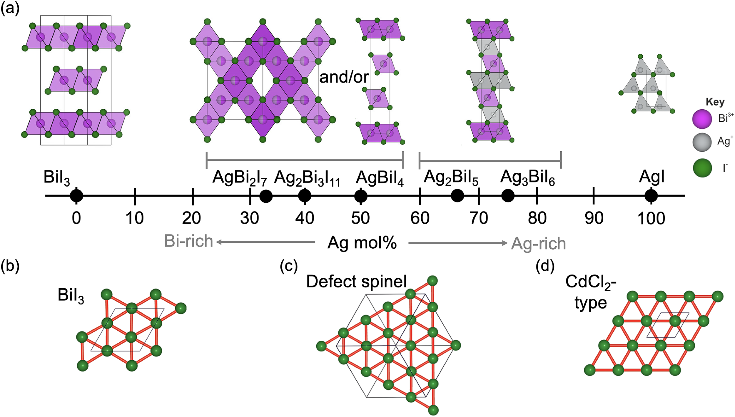
(a) Influence of stoichiometry on the structure of Ag a Bi b I a +3b compounds. Adapted with permission under the terms of the CC-BY license from Sansom et al. 29 Copyright 2021, The Authors. Iodide sub-lattice of (b) BiI3, (c) AgBiI4 (defect-spinel structure), and (d) AgBiI4 (CdCl2-type structure). Reproduced under the terms of the CC-BY license from Sansom et al. 44 Copyright 2017, The Authors.
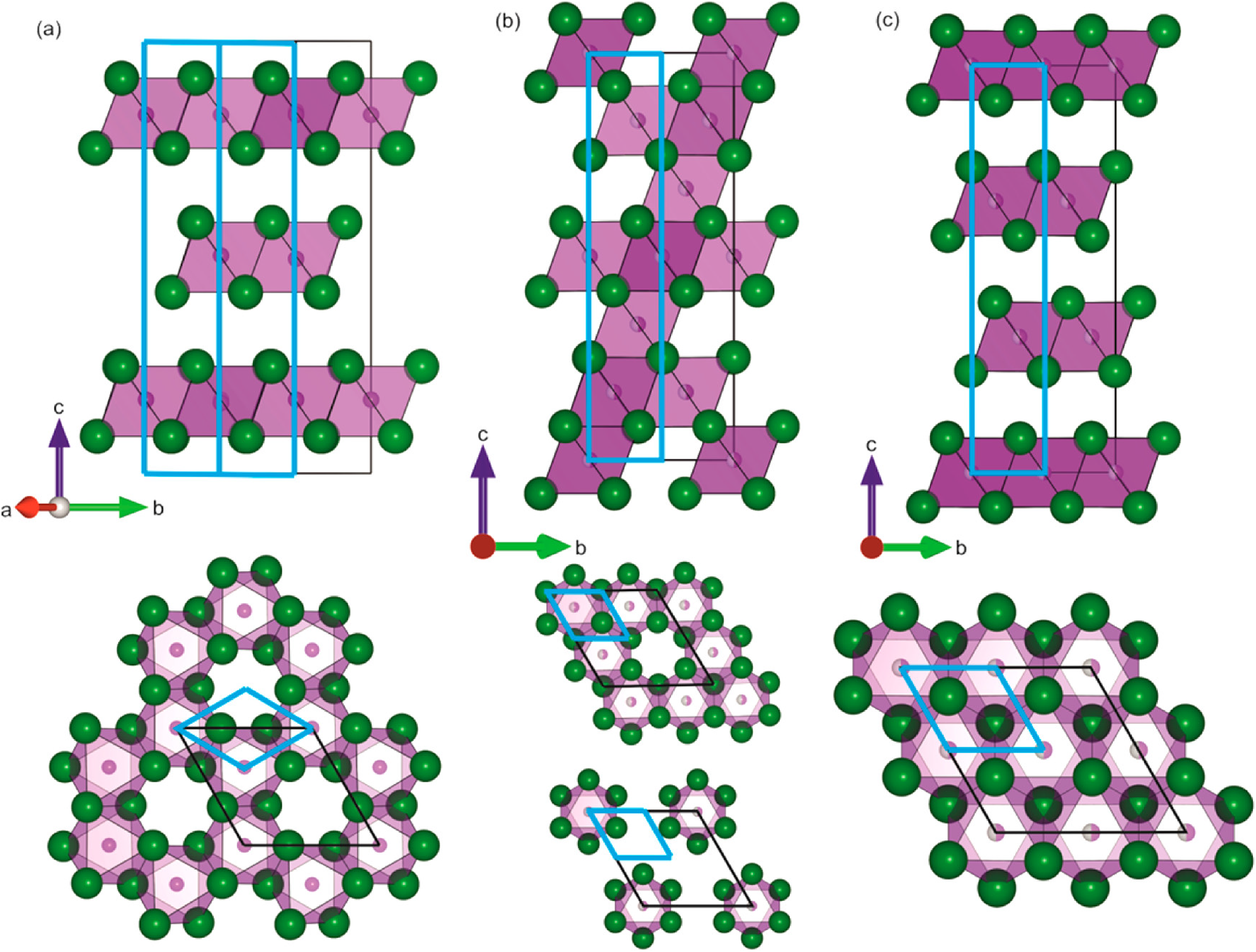
Comparison of the crystal structures of (a) BiI3, (b) AgBiI4 with the defect-spinel structure, and (c) AgBiI4 with the CdCl2-type structure. Reproduced under the terms of the CC-BY license from Sansom et al. 44 Copyright 2017, The Authors.
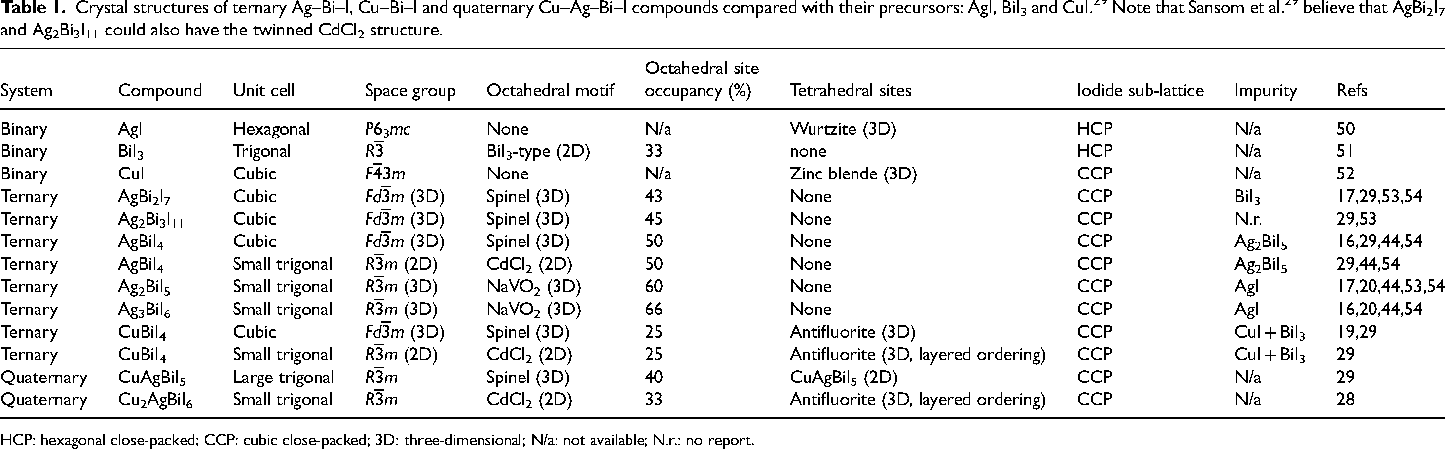
HCP: hexagonal close-packed; CCP: cubic close-packed; 3D: three-dimensional; N/a: not available; N.r.: no report.
The powder diffraction pattern for AgBiI4 can also be explained with a CdCl2-type structure. Therein, there are also one-half of the octahedral holes overall occupied with Ag+ and Bi3+. But this time, a 2D rather than 3D structure is adopted, as illustrated in Figure 3(c). In layer 1, all of the octahedral holes are occupied, while in layer 2, none of the octahedral holes are occupied. It is likely that the Bi-rich compounds can also be explained by a CdCl2 structure, although this is yet to be proven. 29 As the materials become Ag-rich, the extra Ag+ cations partially occupy the octahedral holes in layer 2, and this gives rise to a 3D NaVO2-type structure (Figure 2(a)). Across all of these structures, from BiI3 to Ag-rich Ag–Bi–I compounds, all BiI6 and AgI6 octahedra are edge-sharing, and all tetrahedral holes remain vacant. 29
In addition to these commonly reported structures, Turkevych et al.
21
proposed that the structure of all Ag
a
Bi
b
I
a
+3b compounds can be described based on the NaVO2-type structure, and not just the Ag-rich compounds. In this model, each octahedral hole is comprised of a mixture of Ag+, Bi3+ and vacancies, with a different ratio of these species in layers 1 and 2. All combinations of these species and vacancies in each layer are shown in Figure 4(a), with each point representing a distinct material. The stoichiometries that lead to the smallest unit cells, and which are therefore the most thermodynamically probable, are the Ag3BiI6, Ag2BiI5, AgBiI4 and AgBi2I7 compounds. These match the common stoichiometries reported (Figure 2(a)). It was on this basis that Turkevych et al.
20
proposed to call these Ag–Bi–I compounds ‘rudorffites’
20
However, as described above, not all stoichiometries, especially the Bi-rich ones, adopt the R
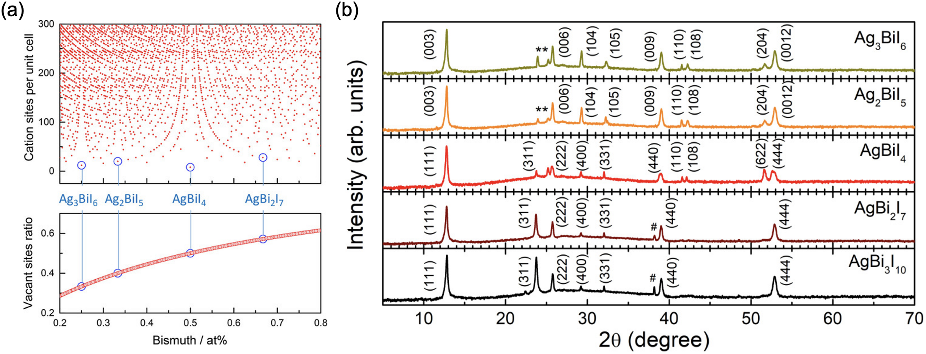
(a) Variation in the number of cation sites per unit cell (top) and vacant sites ratio with the fraction of cations that are bismuth. 20 (b) X-ray diffraction (XRD) patterns of Ag a Bi b I a +3b. Unreacted AgI and BiI3 are marked with asterisk (*) and hash (#) symbols, respectively. 54 Part (a) reproduced with permission from Turkevych et al. 20 Copyright 2017, Wiley. Part (b) reproduced with permission from Bera et al. 54 Copyright 2021, American Physical Society.
In an early report on AgBi2I7 for photovoltaics by Kim et al. in 2016, 22 the authors proposed that the material had a ThZr2H7-type structure, consisting of [AgI6] octahedra and [BiI8] hexahedra. However, [BiI8] hexahedra are unusual. Subsequently, Xiao et al. 49 performed computational studies to show that AgBi2I7 cannot adopt the ThZr2H7-type structure with [BiI8] hexahedra, as it was found to be thermodynamically unstable. Rather, the defect-spinel structure is much more likely.
Finally, a current challenge is that the stoichiometry reported for Ag–Bi–I compounds is usually based on the molar ratio of the precursors used in solution processing. However, it is difficult to clearly distinguish between these stoichiometries because of the high degree of similarity in their X-ray diffraction (XRD) patterns. For example, in the series of Ag–Bi–I compounds shown in Figure 4(b), 54 all Ag-poor compounds have (111), (311), (222), (400), (331), (440) and (444) peaks that are all at similar Bragg angles. The Ag-rich compounds have (003), (006), (104), (009), etc. peaks in similar positions, and these in turn are in similar positions to those of their Ag-poor counterparts (e.g. (111) peak for Ag-poor and (003) peak for Ag-rich compounds). Compounding the difficulties in distinguishing between stoichiometries is the presence of phase impurities in many Ag-poor and Ag-rich materials, such as BiI3 (denoted in Figure 4(b) by a #), and AgI (denoted in Figure 4(b) by an *),20,56 as shown in Table 1. Therefore, it is essential to directly measure the stoichiometry both in the bulk and at the surface, such as through Rutherford backscattering spectrometry and X-ray photoemission spectroscopy, respectively. 57 Identifying phase separation, or how uniformly distributed the Ag and Bi cations are, will be essential to understand in order to control the reproducibility of films.
Electronic structure and optical properties
Figure 5 shows the band structure and density of states (DOS) of Ag–Bi–I compounds from first-principles density functional theory (DFT) calculations. Figure 5(a) 58 and (b) 56 shows that the Ag 4d and I 5p orbitals are the main contributors to the upper valence band (VB), while the lower conduction band (CB) is mainly comprised of I 5p and Bi 6p orbitals for all Ag–Bi–I semiconductors. From these DFT calculations, it can be seen that the curvature of the band extrema for Ag-rich Ag3BiI6 in Figure 5(b) is much larger than the curvature of AgBiI4 (Figure 5(c)) 44 and Ag-poor AgBi2I7 (Figure 5(d)). 59 As the electron (me*) and hole (mh*) effective masses are inversely proportional to the curvature of the band edges, 60 this would suggest that Ag3BiI6 has lower effective masses than Ag-poor materials, and therefore higher upper limits in mobility. Lower effective masses also have beneficial ramifications on other important properties, such as longer diffusion lengths, lower exciton binding energies, and smaller capture cross-sections for charged defect states through lower Sommerfeld factors.2,35 Indeed Crovetto et al. 38 found that Ag3BiI6 has low effective masses down to 0.4m0 for both electrons and holes along the ab-plane (where m0 is the rest mass of an electron), while AgBiI4 has electron and hole effective masses of 0.6–0.8m0 and 0.9–1.0m0, respectively, for the cubic defect-spinel polymorph, and 1.3m0 and 1.8m0, respectively, for the CdCl2-type polymorph. 44
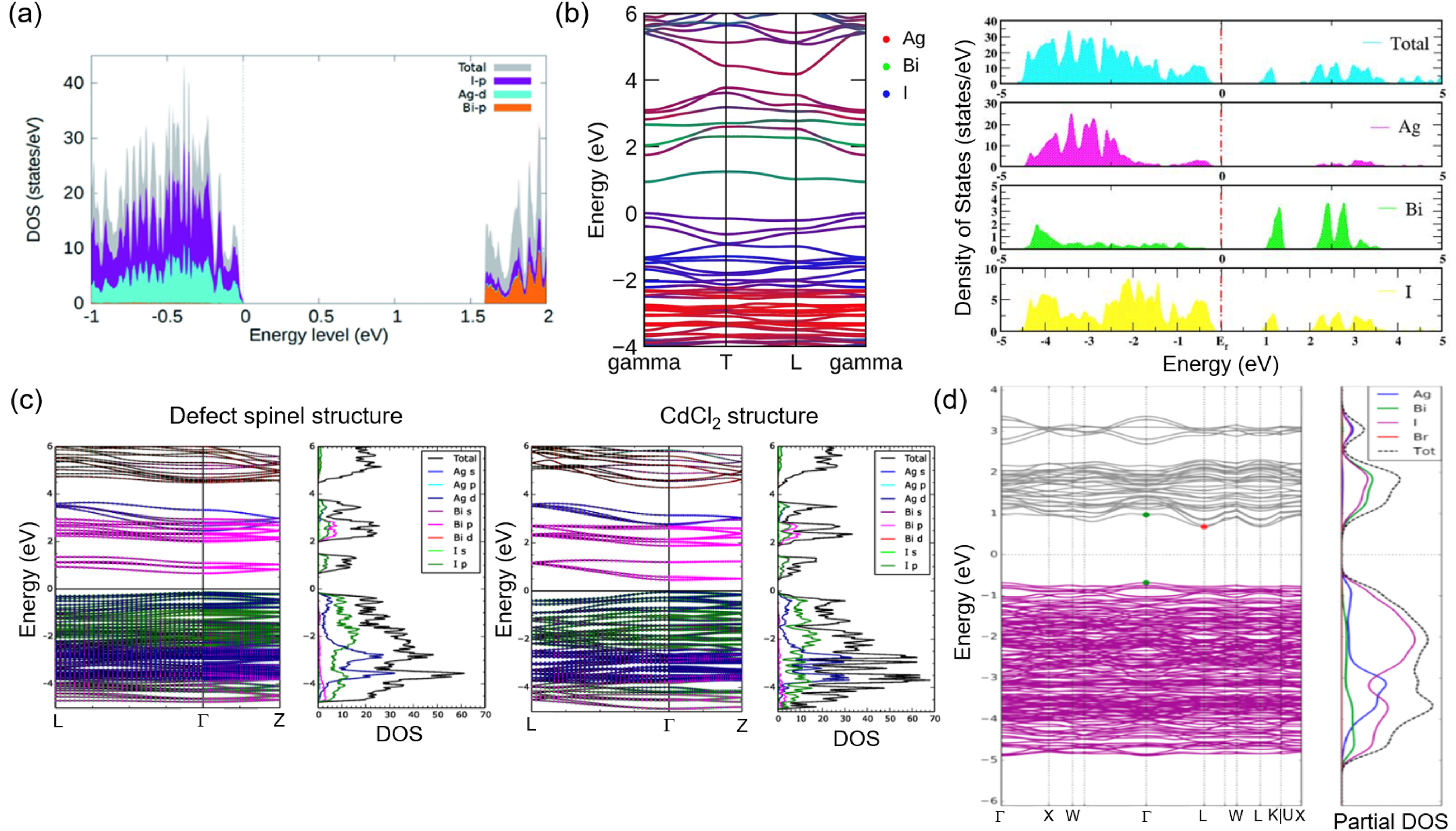
Total and orbital-projected DOS of (a) Ag2BiI5, (b) Ag3BiI6, (c) AgBiI4 in the defect-spinel (left) and CdCl2-type (right) structures, and (d) AgBi2I7 obtained from DFT calculations. For (b), (c) and (d), the band diagrams are also shown. Part (a) reproduced with permission from Park et al. 58 Copyright 2021, The Royal Society of Chemistry. Part (b) reproduced under the terms of the Creative Commons CC-BY license from Kulkarni et al. 56 Copyright 2021, The Authors. Part (c) reproduced under the terms of the CC-BY license from Sansom et al. 44 Copyright 2017, The Authors. Part (d) reproduced with permission from Wu et al. 59 Copyright 2019, American Chemical Society.
Furthermore, Ag–Bi–I semiconductors have shown good optical absorption coefficients (α) > 104 cm−1 in the visible wavelength range, 61 although the exact value for α varies with the stoichiometry.
Absorption coefficients have been reported to reach as high as 105 cm−1 for Ag3BiI6 prepared by iodising sputter-deposited Ag2Bi films (Figure 6). 38 However, currently, the absorption spectra of Ag–Bi–I thin films have been found to have long Urbach tails (e.g. see Figure 6).44,61 This is indicative of a relatively high level of crystal structure disorder. This disorder may be caused by an inhomogeneous distribution of the Ag+ and Bi3+ cations, regions of low crystallinity in the solution-processed samples, strong electron–phonon coupling, or point defects, such as BiAg anti-sites.62,63
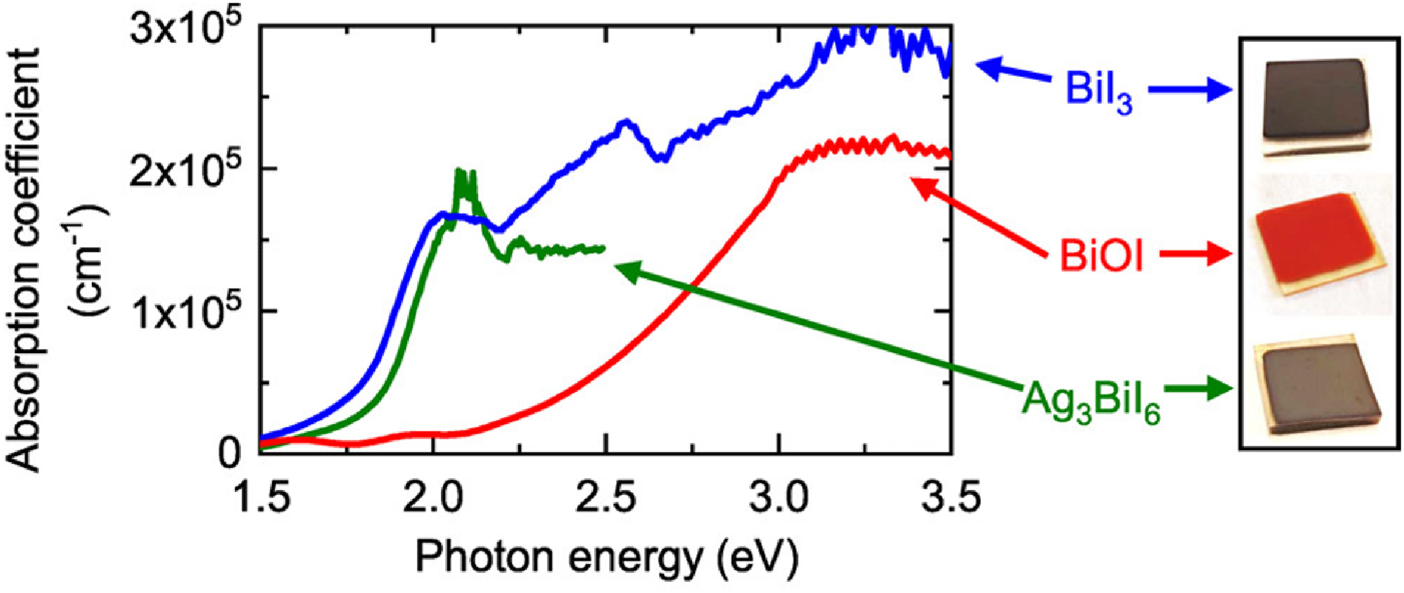
Absorption coefficient of Ag3BiI6 thin films compared with BiI3 and BiOI. Reproduced with permission from Crovetto et al. 38 Copyright 2020, American Chemical Society.
Band positions
The band positions of Ag–Bi–I compounds are shown in Figure 7 in comparison with common electron transport layers (ETLs) and hole transport layers (HTLs) used in solar cells. It can be seen that these band positions are influenced by the stoichiometry. The upper VB is mainly comprised of Ag 4d and I 5p states (with a small contribution from Bi 6s states), whereas the lower CB is mainly due to Bi 6p and I 5p states (Figure 5). Given that Ag 4d is closer to the vacuum level than Bi 6s, the increased Ag 4d character of the VB in Ag-rich compounds may cause an upward shift in the valence band maximum (VBM).54,64 By contrast, the CB minimum (CBM) shifts down for Bi-rich compositions (Figure 7), and this may be due to the strong Bi 6p character of the lower CB. 64 In particular, as a heavy-metal element, Bi has strong spin–orbit coupling, and a stronger Bi 6p character may lead to the CB DOS shifting down into the bandgap as a result. The Eg values of Ag–Bi–I compounds can change from 1.86 to 1.95 eV when the stoichiometry changes from Ag-poor to Ag-rich.54,64 Despite the strong influence of stoichiometry on the band positions of Ag–Bi–I compounds, DFT calculations have shown that a direct bandgap is maintained in both the defect-spinel and CdCl2-type polymorphs of AgBiI4 (Figure 5(c)), as well as in Ag2BiI5 (Figure 5(a)). In both cases, the VBM and CBM remain at the Γ point. However, in AgBi2I7, the bandgap becomes indirect (Figure 5(d)), as the VBM remains at the Γ point, but the CBM shifts to the L point. 59
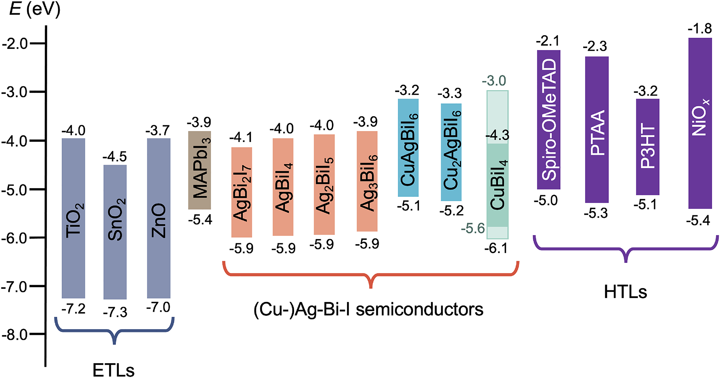
Band positions of Ag–Bi–I, CuBiI4, and quaternary Cu–Ag–Bi–I compounds compared to the energy extrema for the common electron (ETLs) and HTLs used in solar cells. Band positions were obtained from the literature.35,64–72 Please note that Lu et al. 45 and Zhang et al. 67 reported different electron affinities and ionisation potentials for CuBiI4 (3.0 and 5.7 eV by Lu et al., and 4.3 and 6.1 eV by Hu et al. 66 and Zhang et al. 67
Charge-carrier properties
An important question is whether the nature of charge carriers in Ag–Bi–I compounds is more free-carrier-like, or more exciton-like. The exciton binding energy (Eb) of Ag–Bi–I materials was studied by Buizza et al. 62 and Ghosh et al. 27 Although both groups used the Elliott model fitting to their measured optical absorption spectra to obtain Eb, the values determined were very different. Buizza et al. 62 obtained an Eb value of 27 meV for AgBiI4 (implying most charge carriers are free), whereas the value determined by Ghosh et al. 27 for the same material was 260 meV (implying excitons dominate the material). In the same work and using the same method, Ghosh et al. 27 determined the Eb for Ag2BiI5 to be 150 meV. More detailed studies are therefore needed to understand the nature of charge carriers in Ag–Bi–I materials, such as through magneto-optical spectroscopy measurements, 73 measurements of the fluence-dependence of the photoluminescence (PL) peak intensity, or calculations of Eb using a high level of theory. Nevertheless, the Eb values found so far are higher than in LHPs (approximately 20 meV or lower). 73 This may be due to the higher effective masses found in Ag–Bi–I (ranging from 0.4m0 to 1.8m0,38,44 see the ‘Electronic structure and optical properties’ section, compared to ∼0.1–0.2m0 for 3D LHPs 2 ).
Another important factor that complicates charge-carrier transport in Ag–Bi–I materials is the strong interaction between charge carriers and phonons that leads to carrier localisation, in which the wave function of the charge carrier is confined to a unit cell or smaller.62,63 As a result, charge carriers can only move in the bulk of the compound through thermally activated hopping between adjacent sites, which severely limits mobility.
At the same time, it has been found that the stoichiometry can influence the optoelectronic properties. A comparison between AgBiI4 and Ag2BiI5 made by dynamic hot casting showed that as the fraction of Ag increased, there was an increase in the mobility from 1.7 ± 0.3 to 2.3 ± 0.3 cm2 V−1 s−1 (as determined from Hall measurements), along with an increase in the charge-carrier lifetime from 87 ± 5 ns to 133 ± 11 ns (as determined from transient absorption spectroscopy). 27 Turkevych et al. 21 suggested that the longer charge-carrier lifetime and higher mobility in the Ag-rich compounds may arise from fewer recombination centres (e.g. Bi0 – see the ‘Solar cells’ section for a more detailed discussion). 20
Compositional engineering
Tuning the composition of materials is an effective method to adjust their properties. For example, mixing together different cations into the cuboctahedral site of LHPs has led to materials that are more stable and efficient than the prototypical methylammonium lead iodide (MAPbI3). 74 Similarly, there have been several works investigating the inclusion of additives in Ag–Bi–I materials to tune their optical properties and defect density. 36 Figure 8 shows the examples of alloying Sb into the pnictogen site of AgBi2I7, 26 and Br 59 and S 75 into the anion site of AgBi2I7 and Ag3BiI6, respectively. In all three examples, XRD and composition measurements confirmed the incorporation of the additives into the materials.26,59,75 Furthermore, the thin film absorbers in all cases were prepared by spin coating the precursor solution (using N,N-dimethylformamide (DMF), dimethyl sulfoxide (DMSO), or a mixture of both) inside a glovebox, and annealing at 90 °C to 150 °C.26,59,75
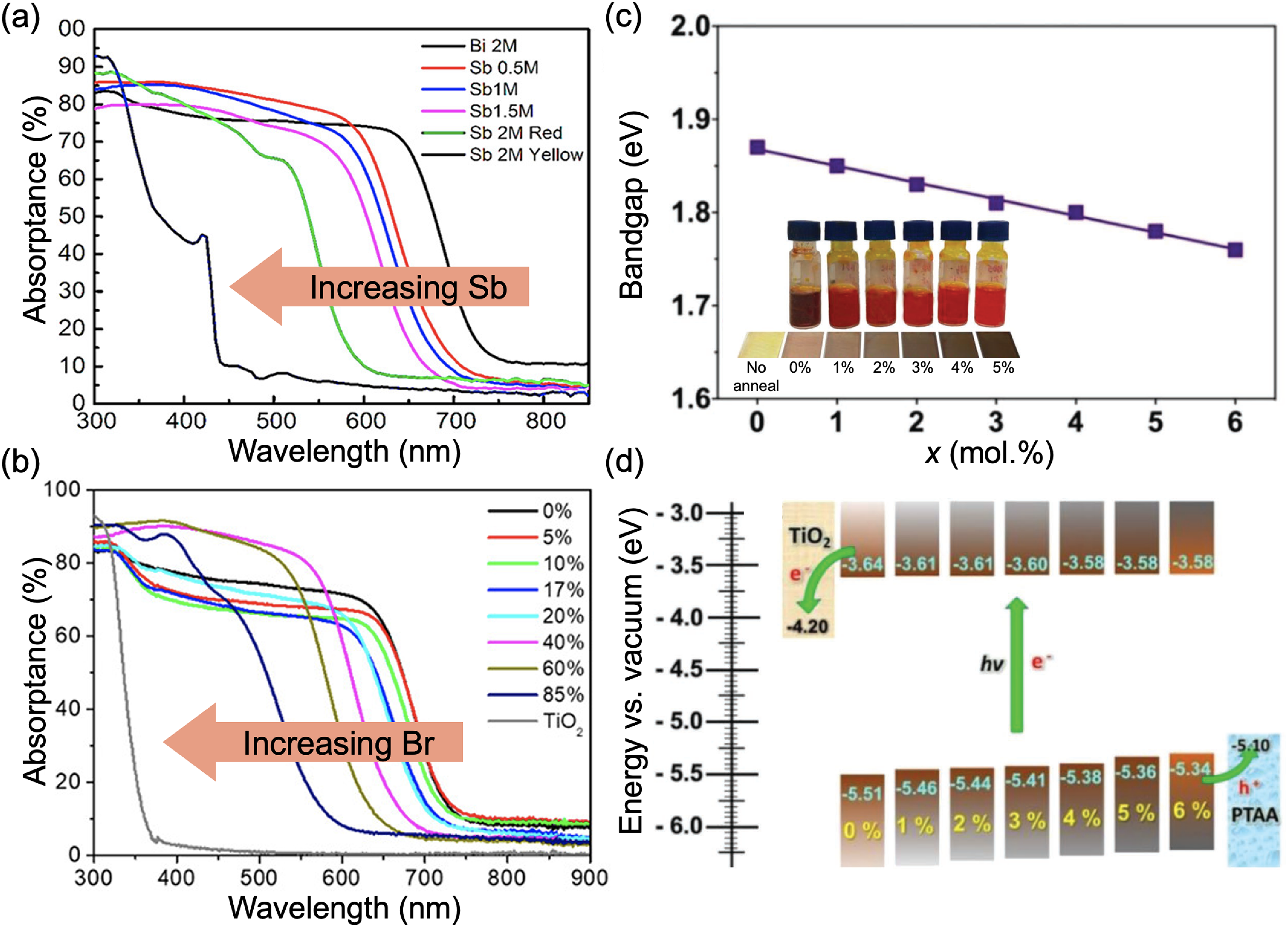
Compositional engineering in Ag–Bi–I. Absorbance of AgBi2I7 films with increasing (a) Sb content, and (b) Br content. Part (a) reproduced under the terms of the CC-BY license from Zhu et al. 26 Copyright 2020, The Authors. Part (b) reproduced with permission from Wu et al. 59 Copyright 2019, American Chemical Society. Effect of S alloying in the anion site of Ag3BiI6 on (c) the optical bandgap, Eg (photographs of precursor solutions and films inset) and (d) band positions. Parts (c) and (d) reproduced with permission from Pai et al. 75 Copyright 2019, Wiley.
Incorporating Sb into AgBi2I7 results in an increase in the indirect bandgap from 1.61 eV (0% Sb) to 1.98 eV (100% Sb), as shown in Figure 8(a). Computational analyses showed that this was due to the higher spin–orbit coupling for Bi compared to Sb. The pnictogen valence p orbitals make a strong contribution to the DOS in the CB, and replacing Bi with Sb results in the DOS extending less into the bandgap due to reduced spin–orbit coupling. 26 Zhu et al. 26 also investigated the effects of pnictogen chemistry on the Urbach tail of these AgBi2−xSb x I7 films by calculating the ‘near edge absorptivity ratio’ (NEAR). NEAR is defined as the square root of α at the bandgap divided by α at an energy 2% larger the bandgap, with the value of 2% being arbitrarily chosen. It was found that alloying Sb into AgBi2I7 leads to a reduction in the NEAR value, which was attributed to a reduction in the density of defect states in the bandgap. 76
Similarly, incorporating Br into the anion site of AgBi2I7 broadened the bandgap (Figure 8(b)). 59 Furthermore, Wu et al. 59 found that alloying 10 at.% Br in AgBi2I7 led to more uniform films with a lower pinhole density. The photostability was also found to be improved, and this could be due to Br alloying improving film formation to give rise to lower defect densities. 59
At the same time, the bandgap of Ag–Bi–I materials, at approximately 1.9 eV, is too wide for single-junction photovoltaic applications under 1 sun illumination. It is therefore important to also find routes to lower the bandgap, and Pai et al. 75 reported that this can be achieved through S incorporation. As can be seen from Figure 8(c), increasing the fraction of S in the precursor solution resulted in a reduction in the bandgap of Ag3BiI6 from 1.87 eV (0% S) to 1.76 eV (6 at.% S), leading to darker films. This reduction in bandgap came about due to a lowering of the ionisation potential (Figure 8(d)), which was likely due to an increase in the S 3p character of the VBM. 75 That is, the S 3p orbital has a lower energy than the I 5p orbital, and is closer to the Ag 4d orbital energy. The upper VB is dominated by the hybridisation between Ag 4d and anion p orbitals, and increasing the S 3p character would increase the repulsion between Ag 4d and the anion p orbital, leading to an antibonding orbital at the VBM with lower energy, thus shifting the VBM closer to the vacuum level. The effects on photovoltaic performance are discussed later in the ‘Using additives to improve photovoltaic performance’ section.
The inclusion of Cs additives to AgBiI4 by solution processing has also been investigated. 77 From XRD measurements, it was found that these materials adopted a cubic defect-spinel structure and that including 1% and 5% Cs+ in the precursor solution led to an improvement in crystallinity, along with an increase in absorbance, PL intensity and PL lifetime. Further increasing the concentration of Cs+ to 10% in the precursor solution resulted in a phase impurity appearing in the resulting films. 78 In these studies on Cs additives, it is uncertain as to where in the lattice Cs+ is incorporated, but Wang et al. 77 speculate that Cs+ and other alkali additives may occupy interstitial sites.
The inclusion of Cs and Sb additives into Ag2BiI5 has also been investigated,77,79 and it was found that larger grains could be formed, especially with the use of Sb additives. As a result, the Urbach energy was decreased, accompanied by a reduction in the bandgap. 79
Materials stability
Ag–Bi–I compounds have a negative formation enthalpy under ambient conditions, meaning that they are thermodynamically stable. 56 Given that they are free from organic constituents, Ag–Bi–I compounds have demonstrated phase stability in ambient air (30% to 70% relative humidity).30,40 However, there are noticeable impurity issues in Ag–Bi–I materials that can accelerate decomposition. Light illumination can also increase the degradation rate of these materials. In this section, we will discuss how these impurities form, and the processes by which they can cause film degradation. Here, the focus is on materials stability and degradation products, and this discussion is carried on in the ‘Solar cells’ section on photovoltaic device stability.
Many groups have reported Ag–Bi–I thin films to be phase-stable in ambient air. Kulkarni et al. 56 synthesised Ag–Bi–I films with different stoichiometries by solution processing (see Figure 9(a)), and found that when there was a high fraction of the AgI phase impurity, the stability of the resulting photovoltaic devices worsened (Figure 9(b)). Curiously, bright dots were seen in the secondary electron images of all of the films (see Figure 9(c) for an example), and these bright dots have been widely reported in Ag–Bi–I thin films.38,40,56,75 Accounts of the causes, behaviour and consequences of these bright dots have varied in different reports. Kulkarni et al. 56 and Pai et al. 75 believe that these bright dots are due to aggregates of the Ag-rich phase, such as AgI. Crovetto et al. 38 reported that these spots are not present initially in Ag3BiI6 when imaged in scanning electron microscopy (SEM), but appear within seconds of electron beam irradiation. By contrast, we have, at times, observed them to be present initially but disappear over time under beam exposure. Kulkarni et al. 56 reported that they only found bright dots to be present at the Ag–Bi–I/TiO2 interface for the AgBi2I7 and Ag2BiI5 samples, whereas the Ag3BiI6 devices had bright dots at the Ag–Bi–I/P3HT/Au interfaces and layers (where P3HT is poly(3-hexylthiophene-2,5-diyl)). This was believed to indicate an accumulation of AgI at the hole-extracting electrode, resulting in poorer photovoltaic performance. Kulkarni et al. 56 also believed that the excess of Ag and I present in these aggregates resulted in the release of Ag+ cations and I− anions that migrated through to the top Au electrode, enhancing the degradation of the device. Notably, this decrease in performance only occurred after incorporating the Ag–Bi–I film into a photovoltaic device. Ag3BiI6 films made into devices fresh versus after storing in the air for 2 weeks before being made into devices exhibited very similar performance and stability (Figure 9(d)). This suggests that ionic species are only released after fabricating the interfaces with the HTL and Au, and may also be accentuated by the application of an electric field. 56 Zhu et al. 40 also observed that Ag–Bi–I films remained stable under storage without an electric field applied, despite the presence of bright dots on the surface of the films.
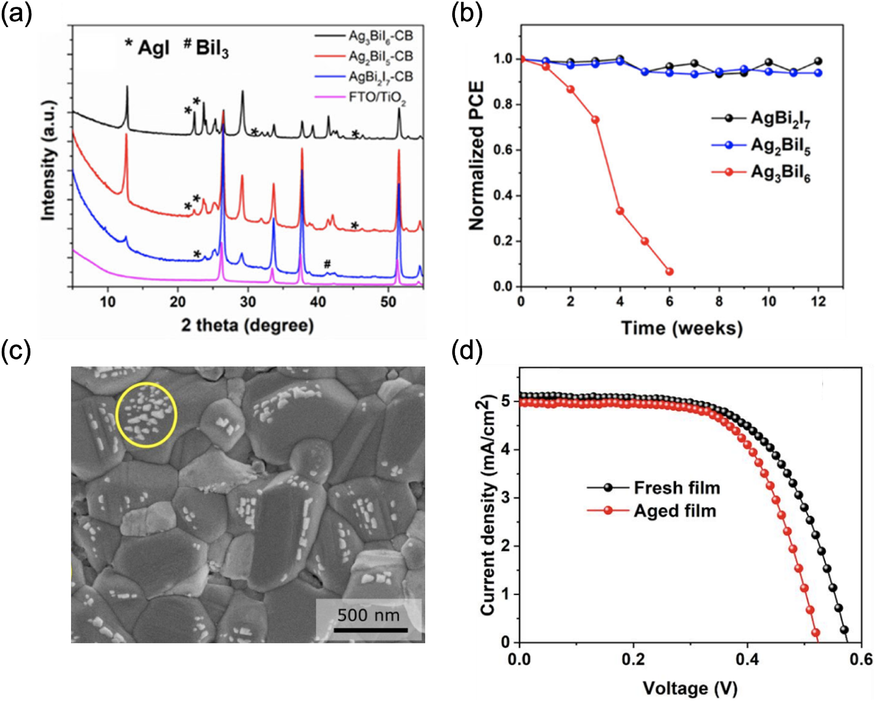
Effect of air exposure on the performance of Ag–Bi–I thin films. (a) XRD pattern and (b) normalised PCE of Ag–Bi–I thin films used in photovoltaics. The XRD patterns were taken in air on fresh samples. (c) Top-down SEM image of an Ag3BiI6 thin film giving an example of bright spots that sometimes appear in the secondary electron image. (d) Current density–voltage curves of devices made from Ag3BiI6 that were fresh, and aged in air for 2 weeks. For the aged samples, the P3HT HTL and Au were only deposited over the Ag–Bi–I films after the 2-week ageing period. Parts (a), (b) and (d) are reproduced under the terms of the CC-BY license from Kulkarni et al. 56 Copyright 2021, The Authors. Part (c) reproduced with permission from Crovetto et al. 38 Copyright 2020, American Chemical Society.
Cu–Bi–I compounds
CuBiI4 and Cu2BiI5 were first reported decades ago, 80 with the structure for CuBiI4 later being solved by the same author. 19 Despite this, the first CuBiI4 solar cell was only published in 2018. 67 There are a handful of works on Cu–Bi–I semiconductors for photovoltaic applications.66,67,81 Cu–Bi–I compounds have bandgaps in the visible wavelength range. In addition, Cu–Bi–I compounds have promising photo- and air-stability, in which the photovoltaic performance was maintained after 30 days of air and 1-sun exposure. Apart from CuBiI4, there have also been reports on Cu3BiI6 solar cells, which exhibited little hysteresis. 82 But currently, CuBiI4 is the material that has been investigated the most, and we will therefore focus on this compound. This section covers the crystal structure, band structure and optoelectronic properties of CuBiI4.
Crystal structure of Cu–Bi–I
Structural investigations into ternary Cu–Bi–I compounds have also mostly been made using single crystal and powder samples.19,28,80,83 Fourcroy et al. 19 prepared CuBiI4 single crystals by melt crystallisation. Sansom et al. 28 and Das et al.83 also used melt crystallisation, but prepared powders instead. All three groups reported the use of rapid quenching in water from a temperature of 350°C instead of slow cooling to room temperature.19,28,80,83 Sansom et al. 28 found that unlike quaternary Cu–Ag–Bi–I materials prepared using similar methods (see later in the ‘Particular considerations for the synthesis of quaternary Cu–Ag–Bi–I compounds’ section), the CuBiI4 crystals were too fragile to retrieve, and so relied on powder XRD to solve the structure.
Like the Ag–Bi–I system, CuBiI4 also has a ccp I sub-lattice, and CuBiI4 has the structure shown in Figure 10. 19 But unlike Ag–Bi–I compounds, Cu+ occupies tetrahedral holes rather than octahedral holes because of the smaller ionic radius of Cu+ (74 pm) than Ag+ (129 pm). 84 CuBiI4 still has one-half of the octahedral holes filled, but these are occupied by Bi3+ and vacancies with 50% occupancy each.19,29,83 Cu+ is disordered over all tetrahedral sites, with 9% to 18% occupancy each, and the BiI6 octahedra are edge-sharing with the CuI4 tetrahedra, forming a 3D network (Figure 10).19,29,83 However, Cu+ occupies an extra tetrahedral site compared to spinel structures and therefore does not have a spinel tetrahedral motif, even though its octahedral motif is spinel. 29 Cu+ also occupies tetrahedral holes in CuI, but unlike AgI, the I sub-lattice in CuI is ccp (Figure 10). 29
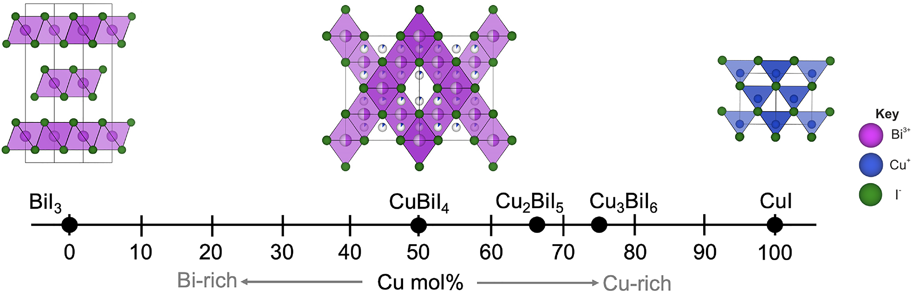
Reported stoichiometries of Cu–Bi–I compounds, and a comparison of the solved structure of CuBiI4 with the structures of BiI3 and CuI. Adapted with permission under the terms of the CC-BY license from Sansom et al. 29 Copyright 2021, The Authors.
Beyond CuBiI4, Cu2BiI5 has been reported to have a hexagonal unit cell. 19 Ramachandran et al. 85 prepared thin films of Cu2BiI5 and, by comparing their measured pattern with reference patterns, agreed that this material has a hexagonal structure. However, more detailed structural analysis using high-quality powder or single-crystal XRD patterns should be made. Baranwal et al. 82 also reported the synthesis of Cu3BiI6, but the structure of this material has not yet been solved.
Apart from these structures, Wang et al.
86
also suggested, based on computational analyses, that CuBiI4 could form two P
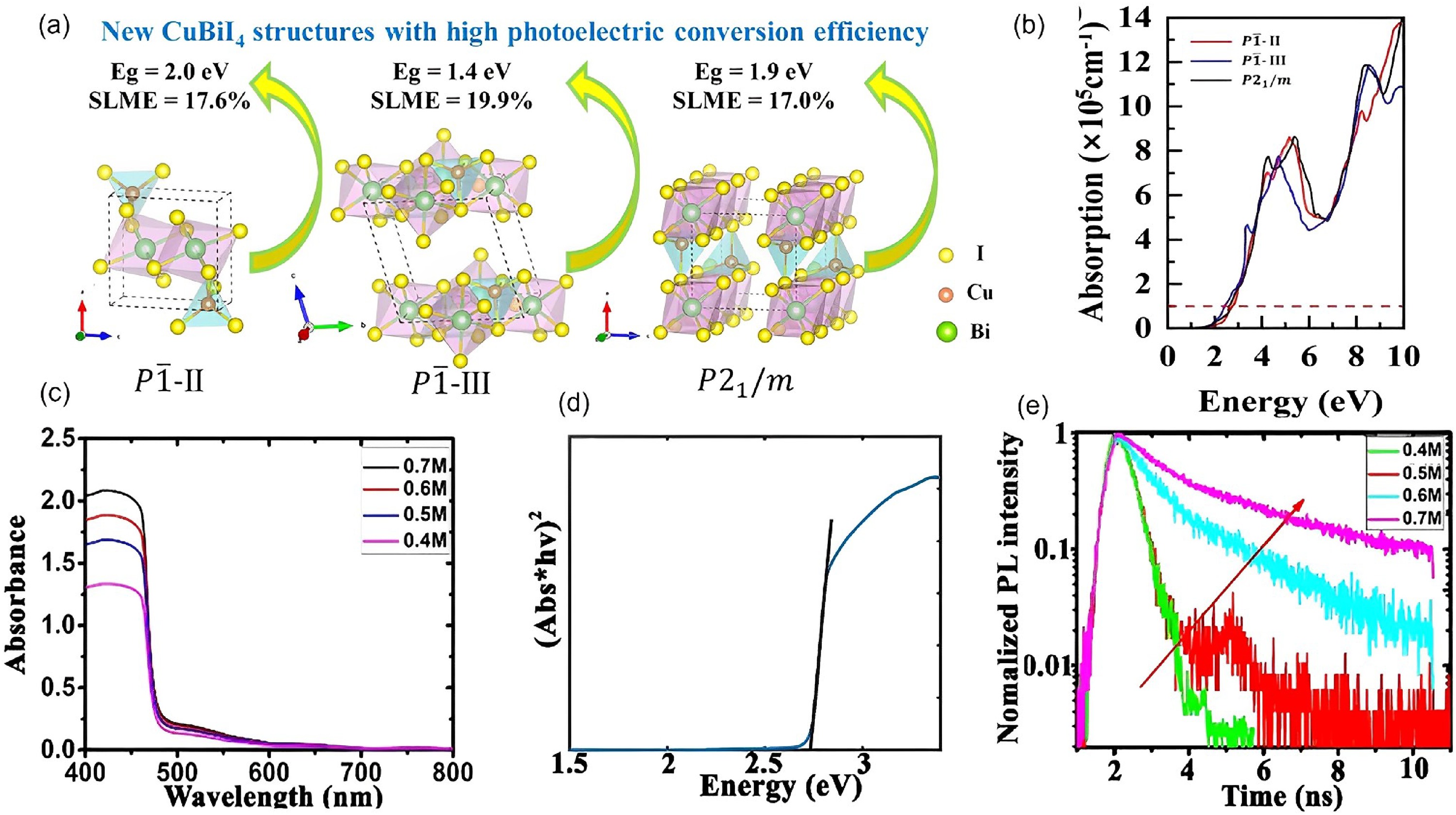
Properties of CuBiI4 from computations and experiment. Computations: (a) predicted structures of CuBiI4: P-II, P
Optoelectronic properties and band positions
From the computational work by Wang et al.,
86
CuBiI4 with the theoretical P
Experimentally, a handful of groups have reported the synthesis of CuBiI4 thin films by spin coating,66,81 as well as by iodising sputter-deposited Bi/Cu alloys. 67 The absorption spectra of CuBiI4 thin films prepared by Hu et al. 66 are shown in Figure 11(c), where it can be seen that the absorption onset remains the same despite changing the precursor concentration and therefore the thickness of the films. However, the direct bandgap found was determined to be 2.67 eV by Hu et al. 66 (Figure 11(d)), which would imply a very low electron affinity (Figure 7). It should be noted that the diffraction pattern of these Cu–Bi–I films did not match well with the reference pattern for CuBiI4, with some peaks offset and many peaks missing (possibly due to preferred orientation). 66 In more recent work, Qu et al. 81 and Zhang et al. 67 reported a bandgap of 1.84 eV, with an electron affinity more in line with other Cu–Ag–Bi–I semiconductors at −4.3 eV (Figure 7). Consistent with these reports, Qu et al. 81 measured a PL peak at 683 nm wavelength (1.82 eV).
Charge-carrier properties
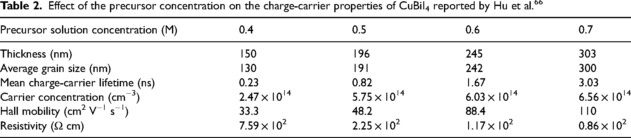
Hu et al. 66 found that as the thickness of CuBiI4 thin films increased, both the Hall mobility (Table 2) and PL lifetime (Figure 11(e)) increased, owing to an increase in grain size (Table 2) and reduced non-radiative recombination. It should be noted, however, that the Hall mobility values reported are substantially higher than expected from a solution-processed thin film. For example, Sansom et al. 28 reported that the quaternary compound, Cu2AgBiI6, in polycrystalline thin film form has a mobility of only 1.7 cm2 V−1 s−1. More in-depth investigations into the mobility of CuBiI4 should be made, especially for single crystal samples to determine the upper limits in mobility.
Effect of the precursor concentration on the charge-carrier properties of CuBiI4 reported by Hu et al. 66
The charge-carrier properties of CuBiI4 were also examined by transient photovoltage measurements. 88 From these, a positive signal was observed, implying that the films were n-type. The recombination lifetime of CuBiI4 thin films was found to exceed 3 ns, which is consistent with the PL lifetime measurement from Hu et al. 66 (Figure 11(e)), and implies that the material is suitable for further efforts to develop them into photovoltaics. 89
Materials stability
There have been some stability studies on CuBiI4 thin films and powders (Figure 12), with mixed conclusions. Sansom et al. 28 synthesised phase-pure powders by heating BiI3 and CuI powders in silica ampoules followed by rapid quenching. When samples were stored in air for 3 weeks at both room temperature and −20°C, they were found to decompose to BiI3 and CuI precursors. Cooling powders to −20°C slowed this decomposition process. Sansom et al. 28 concluded that CuBiI4 is meta-stable. This is consistent with reports of Fourcroy et al., 80 who stated CuBiI4 only exists above 276°C based on extensive exploratory synthesis within the CuI−BiI3 phase space, although they did not comment on the degradation rate of quenched materials. Using a similar synthesis method, Das et al. 83 prepared a phase-pure ingot of CuBiI4. They found powders exposed to ambient air with standard laboratory lighting for 10 days showed no signs of decomposition as observed via PXRD and thermal conductivity measurements. Furthermore, they found samples heated in the air between 323 K and 398 K for 4 h remained stable as measured using PXRD and ultraviolet–visible (UV–Vis) spectroscopy. 83 Hu et al. 66 synthesised (111)-orientated CuBiI4 thin films by combining spin coating with solvent vapour annealing. After exposing the thin films to air for 42 days, they found no change in the XRD patterns as compared to freshly annealed films. 66 Ramachandran et al. 85 claim to have synthesised Cu2BiI5 thin films for use in photodetector devices. They compared XRD patterns of freshly annealed samples with thin films exposed to air for 30 days. The XRD patterns of the air-exposed samples showed changes in peak intensity ratios, along with the appearance/disappearance of a number of minor peaks. 85
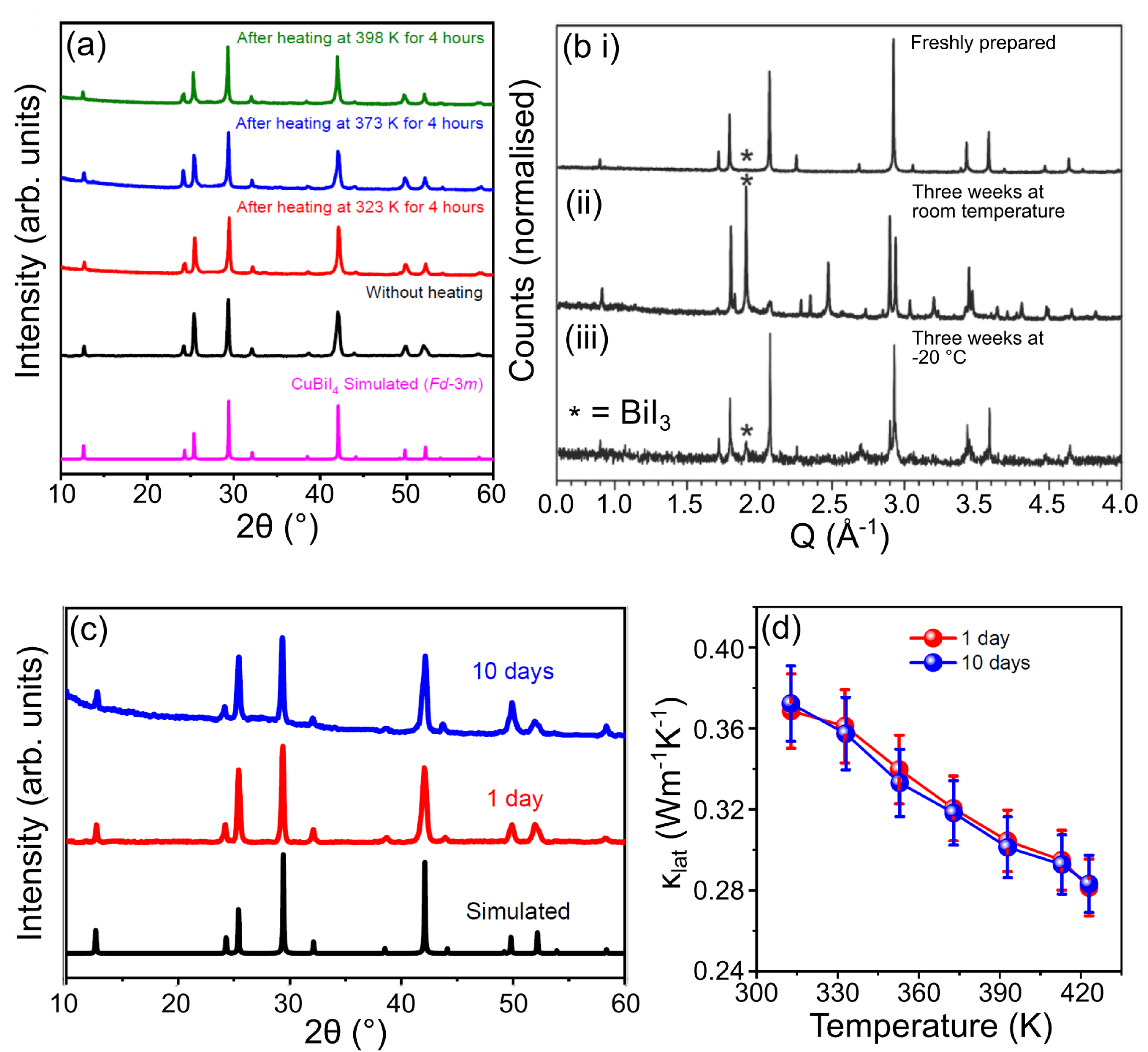
Stability studies of CuBiI4 powder samples. (a) Thermal stability of CuBiI4 after heating for 4 h intervals in an air oven. 83 (b) Powder X-ray diffraction (PXRD) patterns of (i) freshly prepared CuBiI4 powder, and powders stored in air and darkness for three weeks at (ii) room temperature and (iii) −20°C. 28 (c) PXRD patterns and (d) lattice thermal conductivity measurements of CuBiI4 powders stored in open lab conditions for 10 days. Das et al. 83 suggest CuBiI4 is a stable material. However, Sansom et al. 28 believe that it is only meta-stable and degrades to BiI3 and CuI when given enough time. Parts (a), (c) and (d) reprinted (adapted) with permission from Das et al. 83 Copyright 2023, American Chemical Society. Part (c) reproduced with permission under the terms of the CC-BY license from Sansom et al. 28 Copyright 2021, The Authors.
Quaternary Cu–Ag–Bi–I compounds
Crystal structure of Cu–Ag–Bi–I
Sansom et al. 28 reported the exploration of five materials along the AgBiI4–CuI solid solution line: Cux(AgBi)1−xI4 with x = 0 (AgBiI4), 0.09 (Cu0.4AgBiI4.4), 0.2 (CuAgBiI5), 0.33 (Cu2AgBiI6) and 0.6 (Cu6AgBiI10), as shown in Figure 13(a).29,62 The structures of CuAgBiI5 and Cu2AgBiI6 were examined in detail from single crystal and powder XRD measurements.28,29 CuAgBiI5 was found to form a 3D defect-spinel structure, 29 whereas Cu2AgBiI6 has a 2D CdCl2-type structure (Figure 13(a)). 90 This change in phase may account for the large change in lattice parameters and cell volume from x = 0.2 to x = 0.33 (Figure 13(b) 62 ).
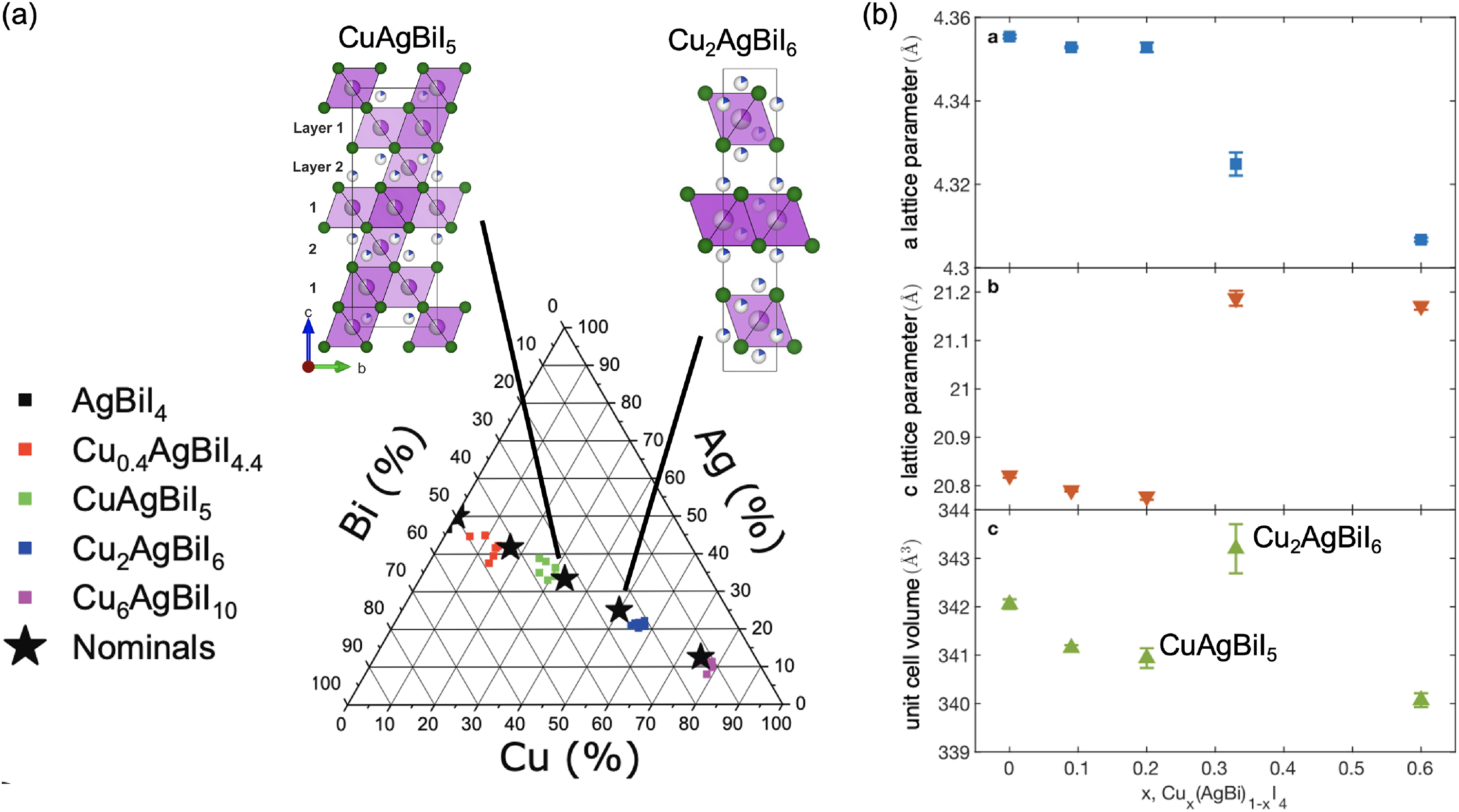
Structure of quaternary Cu–Ag–Bi–I compounds. (a) Nominal and reported compositions of Cu–Ag–Bi–I materials investigated, and (b) the lattice parameters and unit cell volumes of these materials. These are plotted against x in Cu x (AgBi)1−xI4, where x = 0 (AgBiI4), 0.09 (Cu0.4AgBiI4.4), 0.2 (CuAgBiI5), 0.33 (Cu2AgBiI6), 0.6 (Cu6AgBiI10). Adapted with permission under the terms of the CC-BY license from Buizza et al. 62 Copyright 2022, The Authors.
Sansom et al.
29
found that the single crystal XRD pattern of CuAgBiI5 could be solved with the 3D spinel octahedral motif. But unlike AgBiI4, this structure cannot also be described by a twinned CdCl2 structure.
29
Furthermore, Sansom et al.
29
found from fitting the powder XRD pattern that the unit cell is not well described by a cubic unit cell, and instead transformed the cubic unit cell (Fd
For Cu2AgBiI6, Sansom et al. 28 found that the octahedral motif is CdCl2-type, and the occupancies are 30.6% (Bi3+) and 34.7% (Ag+) with the balance vacancies. Cu+ is disordered over all tetrahedral holes, with 17.9% occupancy. 28
Beyond these detailed studies, there have also been reports of CuAgBi2I8 prepared by sputter depositing Bi, Cu and Ag, followed by heating in a I2-rich gas environment (referred to as one-step gas-solid-phase diffusion-induced direct metal surface elemental reaction (DMSER)).
91
From thin film diffraction measurements, it is believed that this material has a defective spinel structure, with a space group of Fd
Particular considerations for the synthesis of quaternary Cu–Ag–Bi–I compounds
Single crystals, powders and polycrystalline thin films of quaternary Cu–Ag–Bi–I compounds have all been synthesised.28,29,58,62,65,91,92 The detailed structural information discussed in the ‘Crystal structure of Cu–Ag–Bi–I’ section above was obtained from single crystal and PXRD. Unlike the synthesis of Ag–Bi–I and CuBiI4 powders, which can be obtained by melt crystallisation,17,18,28 Sansom et al.28,29 reported that CuAgBiI5 and Cu2AgBiI6 needed to be synthesised by solid-state reaction (at 350 °C for a few days) between the binary iodide precursors with fast quenching. This was to avoid compositional inhomogeneities, which occur if a melt is formed or if the product synthesised is cooled down to room temperature slowly.28,29 These complications may arise because of the mobile nature of the elements present, especially at elevated temperatures. In the synthesis of these Cu–Ag–Bi–I powders, Sansom et al.28,29 found that sufficiently large single crystals (∼20 µm along each dimension) could be obtained for single crystal diffraction measurements. In contrast, Park et al. 58 used melt crystallisation by heating the CuI, AgI and BiI3 precursor powders at 450 °C for 12 h. At this temperature, BiI3 melts (melting point of 409 °C), and acts as a solvent for AgI and CuI, which have higher melting points of 558 °C and 606 °C, respectively. 58 However, in this work, the compositional homogeneity was not reported.
There have been a handful of reports of thin film processing of these materials, which have mostly been reported since 2021. Like Ag–Bi–I and LHPs, thin films of Cu–Ag–Bi–I compounds are commonly deposited by solution processing thus far, typically using a mixture of DMF and DMSO as the solvent.28,29,58,62,65,92,93 A challenge is that the binary iodide salts tend to have low solubility in this solvent mixture, or each solvent individually. 93 Thus, groups have reported that the Cu–Ag–Bi–I films are Ag- and Bi-poor compared to the precursor stoichiometry,28,29 and many groups have mixed their solutions at high temperature and sometimes spin coat with the precursor solution still warm to avoid precipitating out the inorganic salts.28,29,62,92 Another strategy employed to overcome this challenge is to add pyridine to the precursor solution, 93 or to directly use pyridine to dissolve CuI before mixing this solution into the DMF/DMSO solution containing the Ag–Bi–I precursors. 28 Indeed pyridine has been found to coordinate with both CuI and BiI3. 94
Finally, as mentioned in the ‘Crystal structure of Cu–Ag–Bi–I’ Section, DMSER has also been used to synthesise Cu–AgBi–I thin films, where the stoichiometry can be tuned through the thickness of the original metal layers sputter deposited. 91 However, in all cases, a thin layer of CuI forms on the surface of the films, and this can act as an HTL, given its wider bandgap and lower ionisation potential compared to Cu–Ag–Bi–I semiconductors. This surface CuI layer can be removed by etching with dilute nitric acid. 91
Optoelectronic and charge-carrier transport properties
Several groups have found that Cu–Ag–Bi–I compounds have high absorption coefficients >105 cm−1 (Figure 14(a)),28,65 which are at a comparable level to the reported absorption coefficients of Ag3BiI6 (see Figure 6). 38 Taking the specific example of Cu2AgBiI6, the absorption coefficient at the band edge substantially exceeds that of MAPbI3 perovskite, as well as the popular elpasolite Cs2AgBiBr6 (Figure 14(a)). Notably, Cu2AgBiI6 exhibited a PL peak at room temperature, albeit red-shifted to 1.71 eV (Figure 14(a)). 28 Sansom et al. 29 also found that CuAgBiI5 has slightly higher absorption coefficients than Cu2AgBiI6, although the PL intensity was weaker. The bandgap of CuAgBiI5 and Cu2AgBiI6 are similar (1.8 and 2.06 eV, respectively).28,29 Fan et al. 91 found that increasing the Cu and I content (to maintain charge neutrality) in DMSER-made Cu–Ag–Bi–I films resulted in a reduction in the bandgap from 1.91 eV (Cu0.6AgBi2I7.6) to 1.78 eV (CuAgBi2I8).
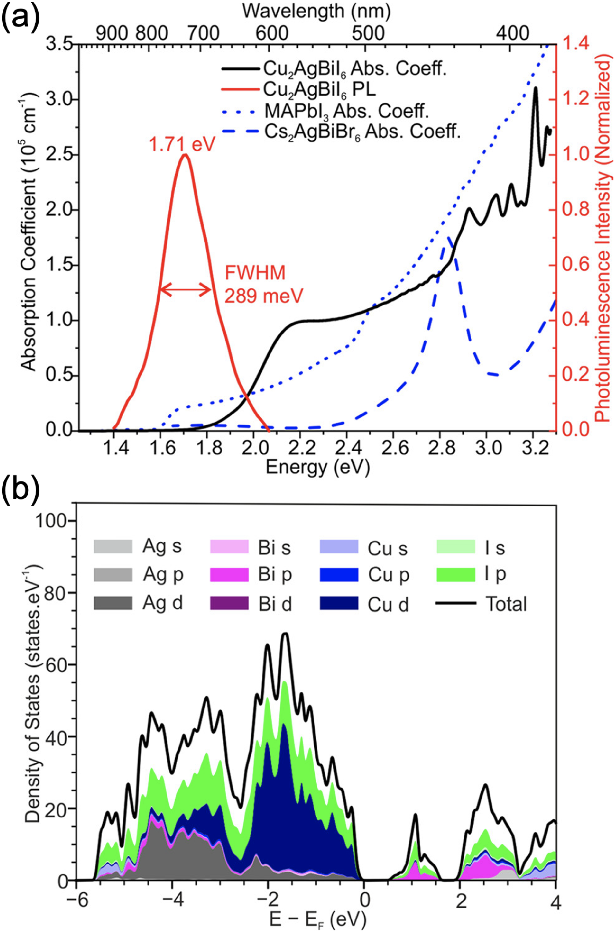
Optical and electronic properties of Cu–Ag–Bi–I compounds. (a) Absorption coefficient (black) and PL spectra (red) of Cu2AgBiI6 thin films compared with the absorption coefficient of MAPbI3 (blue, short dashes) and Cs2AgBiBr6 double perovskite (blue, long dashes). (b) Calculated orbital-projected DOS of Cu2AgBiI6. Reproduced under the terms of the CC-BY license from Sansom et al. 28 Copyright 2021, The Authors.
To better understand the origin of the high absorption coefficients in Cu2AgBiI6, the orbital-projected DOS were calculated (Figure 14(b)). As with all other Ag–Bi–I materials, the upper VB is mainly comprised of Ag 4d and I 5p orbitals, while the lower CB is mainly comprised of Bi 6p and I 5p orbitals. Introducing Cu results in a substantial increase in the DOS in the upper VB due to Cu 3p orbitals (Figure 14(b), blue), with minimal changes in the CB. These changes to the VB DOS result in the high absorption coefficients found in Cu2AgBiI6. 28
From the absorption spectrum of Cu2AgBiI6, it can be seen that there is a small peak just above the absorption onset (Figure 14(a)), which may arise from an excitonic peak. To understand this, Sansom et al. 28 fitted the Elliott model to the absorption spectrum, obtaining an Eb of only 25 meV. The low Eb may be due to the higher band dispersion and lower effective masses in Cux(AgBi)1−xI4 with increasing Cu content. 62
At the same time, there is a significant Stokes shift in the PL peak, that is not consistent with the low Eb. Buizza et al. 62 tested the hypothesis that this large Stokes shift is due to carrier localisation. Using optical pump–terahertz probe (OPTP) spectroscopy, Buizza et al. 62 measured the photoconductivity transients in this material, observing an ultrafast decay in photoconductivity over the first few picoseconds, followed by a slow tail in the decay of the OPTP signal. The initial rapid decay in photoconductivity is characteristic of carrier localisation due to strong electron–phonon coupling, resulting in the charge-carrier wavefunction localising to the order of a unit cell, causing a substantial reduction in mobility (and therefore decrease in photoconductivity). This carrier localisation process was found to be particularly severe in AgBiI4. Intriguingly, increasing the Cu content resulted in an increased tail in the photoconductivity transients, suggesting the presence of more free charge carriers, and an increase in the overall charge-carrier mobility. 62
In addition, Buizza et al. 62 found that increasing the Cu content in Cu4x(AgBi)1−xI4 compounds led to a reduction in the Eb from 27 meV (AgBiI4) to 19 meV (Cu6AgBiI10). Both Buizza et al. 62 and Sansom et al. 90 found the Eb for Cu2AgBiI6 to be 25–27 meV. These values were all obtained from the Elliott model fitting of the optical absorption spectra of these materials as thin films,62,90 and imply that a substantial fraction of the charge carriers at room temperature in these materials are free carriers. Furthermore, Buizza et al. 62 found from OPTP measurements that the photoconductivity signal did not completely decrease to zero instantaneously after photo-excitation, but rather the kinetics changed depending on the Cu content. This is also consistent with free carriers being dominant, since the formation of excitons would lead to the OPTP signal decreasing to zero. Indeed, electron-beam induced current (EBIC) measurements showed that the electron/hole diffusion lengths were short in Cu2AgBiI6 and CuAgBiI5, in the range of 40 to 50 nm, well below the active layer thickness of 120 to 150 nm. 65
Materials stability
Sansom et al. 28 found that while CuBiI4 decomposed to BiI3 and CuI at room temperature, the stability of Cu2AgBiI6 was substantially improved, with no signs of decomposition after a week, even under 1 sun illumination (Figure 15(a)).
Stability of quaternary Cu–Ag–Bi–I compounds. (a) Powder XRD pattern of Cu2AgBiI6 stored in the air in the dark (control) compared to Cu2AgBiI6 stored in a capillary sealed with air and exposed to 1 sun illumination. Both sets of samples were stored for 1 week. These measurements are compared to AgBiI4 stored under equivalent conditions. Reproduced under the terms of the CC-BY license from Sansom et al. 28 Copyright 2021, The Authors. (b) PL spectra of CuAgBiI5 thin films made in an N2-filled glovebox and stored in air for up to 90 min. Part (f) reproduced with permission from Sansom et al. 29 under the terms of the CC-BY license. Copyright 2021, The Authors.
Ambient air exposure has a curious effect on the optoelectronic properties of CuAgBiI5. Like Cu2AgBiI6, there is a large Stokes shift in the PL peak compared to the optical bandgap, which may also originate from carrier localisation (see the ‘Particular considerations for the synthesis of quaternary Cu–Ag–Bi–I compounds’ section). Intriguingly, it was found that the PL peak blue-shifted and became brighter as the CuAgBiI5 film was kept in ambient air (the sample was kept in ambient air in the dark, and measured after 20, 60 and 90 min since being taken to air), as seen in Figure 15(b). 29 This observation was attributed to oxygen passivation of deep traps in the Cu–Ag–Bi–I film and is consistent with the observed increase in PL lifetime after storage in air. 29 On the other hand, after a week of air exposure, CuAgBiI5 changed colour from dark red to yellow, despite no changes in the bulk diffraction pattern, indicating that this material may not be as air-stable as Cu2AgBiI6. 29
Defects and ion migration
One of the key motivations behind the exploration of Bi-based materials is to find compounds that could replicate the defect tolerance of LHPs through similarities in the electronic structure. 89 However, it is questionable as to whether materials in the CuI–AgI–BiI3 phase space are defect tolerant, and indeed we argue later in the ‘Solar cells’ section that they are not.
Efforts to understand and control the defects present in these materials have thus far focussed on the ternary silver bismuth iodide semiconductors. These studies have mostly been on the structural and point defects in Ag–Bi–I thin films by controlling the composition and morphology. However, thus far, there have been no detailed studies into the point defects present (e.g. vacancies or interstitials). Probing these point defects experimentally and computationally would be challenging. Ag–Bi–I compounds are ionic conductors, and ion migration would complicate the use of any capacitance-based method to measure the traps present (such as thermal admittance spectroscopy). 95 Cation disorder makes it difficult to accurately simulate these systems computationally to determine the defect diagrams. Overcoming these challenges will be important to understand what defects are limiting performance, and how the processing and composition of these materials could be optimised in the future. This section discusses the few works that have considered the defects that may be present in Ag–Bi–I semiconductors.
Defects in Ag–Bi–I compounds
Table 3 summarises the carrier type of Ag–Bi–I compounds (made by spin coating with antisolvent dripping), and the point defects that may be present to give rise to this type of conductivity. 54 The Ag-rich materials, Ag3BiI6 and Ag2BiI5, exhibit p-type conductivity, indicating the involvement of acceptor-like point defects, as these compounds have been observed to occur with unreacted AgI.20,56 Ag vacancies (VAg) are therefore a plausible cause of these observations. AgBiI4 and AgBi2I7, on the other hand, showed n-type conductivity. Unreacted BiI3 has been observed in Ag-poor materials,20,56 signifying the presence of I vacancies (VI) in these compounds.
Carrier type, possible defects and likely phase impurities reported so far in Ag a Bi b I a +3b compounds (n.r. = no report). 54
Macroscopic structural defects are also present in Ag–Bi–I thin films. As with other thin films, grain boundaries can act as sites of non-radiative recombination, and pinholes in the film can cause shunting in the vertically structured photovoltaic device. But apart from these structural/macroscopic defects, Kulkarni et al. 56 found that Ag3BiI6 thin films grown by solution processing (and using a chlorobenzene antisolvent) formed voids at the interface with the TiO2 ETL it was deposited onto (Figure 16(a)). It was believed that these voids formed because the chlorobenzene antisolvent could remove excess DMSO solvent, especially at the bottom interface. As a result, Ag3BiI6 only crystallised at the top surface, forming voids at the bottom. 56 Such voids act as sites of non-radiative recombination and limit electron extraction, thus decreasing the photovoltaic performance of these materials, and possibly also decreasing the stability of the devices in air. These voids could be eliminated by depositing Ag3BiI6 without using any antisolvent.
Defects and ion migration in Ag–Bi–I semiconductors. (a) Cross-sectional SEM image of an Ag3BiI6 photovoltaic device, showing voids at the TiO2/Ag3BiI6 interface. (b) Proposed mechanism for Au electrode degradation through the migration of I−, Ag+ and Bi3+ ions through the organic HTL. X-ray photoemission spectra of the (c) Au 4f and (d) Bi 4f core levels, measured on the Au top electrode in the regions that were pristine versus degraded (shown inset in part (c)). Reproduced under the terms of the CC-BY license from Kulkarni et al. 56 Copyright 2021, The Authors.
Ion migration in Ag–Bi–I
Despite Ag–Bi–I originally being investigated as an ion conductor, little is known about ionic conductivity in these materials. The activation energy barrier for Ag+ cation migration has been reported to be 0.4 eV in Ag3BiI6 single crystals made by solvothermal growth, 16 which is similar to the activation energy of I migration (0.44 eV) in lead-halide perovskites. 56 Although Ag–Bi–I semiconductors are thermodynamically favoured to form, Kulkarni et al. 56 found through computations that the degradation of Ag3BiI6 to AgI and BiI3 is also thermodynamically favoured, with a negative enthalpy change of −0.053 eV per formula unit. This is consistent with the presence of AgI and BiI3 phase impurities in the Ag–Bi–I films (see Tables 1 and 3). It is believed that AgI can decompose further to Ag+ and I−. It is proposed that these ionic species, as well as BiI3, can diffuse through the organic HTL (accentuated by the presence of an electric field) and reach the Au electrode (Figure 16(b)). BiI3 can undergo an underpotential deposition reaction on the surface of Au, leading to the formation of Bi0, while Au reacts with the iodide species and likely forms Au+. This proposed mechanism was corroborated by X-ray photoemission spectroscopy measurements on the surface of Au, where a degradation product peak was found from the Au 4f spectra (Figure 16(c)), and Bi0 was found from the Bi 4f spectra (Figure 16(d)). 56 This degradation mechanism was suppressed by increasing the thickness of the HTL. Further work is needed to prove the mechanism by which these species migrate to the Au electrode, but it is suspected that these are facilitated by vacancy defects, as well as the voids present in the film. 56
Applications
Solar cells
Since the first two reports of photovoltaics using Ag–Bi–I semiconductors were made in 2016,21,22 a wide range of deposition methods, fabrication protocols and device structures have been investigated, as shown in Table 4. The highest PCE under 1 sun illumination now reported is 5.56% for Ag3BiI6 compounds with S additives (Table 4), which lowered the bandgap. 75 One sun SLMEs for these materials have been reported for AgBiI4, Ag2BiI5 and CuBiI4, and these SLMEs were found to be 26%, 24% and 17% to 20%, respectively.23,86 We note that the SLME for CuBiI4 was calculated based on computationally determined crystal structures instead of the experimentally solved cubic structure.29,86 Nevertheless, the highest PCEs reported for these compounds (2.8%, 2.6% and 1.12% for AgBiI4, Ag2BiI5 and CuBiI4, respectively, as shown in Table 4) are still well below these SLMEs, showing there to be much room for improvement.
Reported photovoltaic performance of Cu–Ag–Bi–I absorbers. The average values and uncertainties for each performance parameter, along with the performance of the champion device, are shown where available.
RDF: ternary and quaternary compounds in the CuI–AgI–BiI3 phase space; SPC: spin coating; SPC-HC: spin coating with hot casting; AST: antisolvent treatment; SA: solvent annealing; TADB: thermal-assisted doctor blade coating; IM3L: infiltration into mesoscopic three-layer structure; EVAP: evaporation; SPUT: sputtering; I2(V): iodine vapor treatment; BHJ: bulk-heterojunction; c-m-TiO2: compact + mesoporous TiO2; DMSO: dimethylsolfoxide; DMF: N,N-dimethylformamide; BA: n-butylamine; DMA: N,N-dimethylacetamide; CB: chlorobenzene; TL: toluene; IPA: isopropyl alcohol; MB: methylbenzene; EtEt: ethyl ether; Ether: a non-specified ether; EtOH: ethanol; TBP: 4-tert-butylpyridine; ACN: acetonitrile; LiTFSI: lithium bis(-trifluoromethanesulfonyl) imide; [Co]: cobalt(III) complex tris[2-((1H-pyrazol-1-yl)-4-tert-butylpyridine)cobalt(III)tris(bis(trifluoromethylsulfonyl)imide)]; sp: spiro-OMeTAD–2,2′,7,7′-tetrakis(N,N-di-p-methoxy phenylamino)-9,9-spirobifluorene; sp(TFSI)2: 2,2′,7,7′-tetrakis(N,N-di-p-methoxy phenylamino)-9,9-spirobifluorene bis(trifluoromethane) sulfonimide; PTAA: Poly[bis(4-phenyl)(24,6-trimethylphenyl) amine; P3HT: poly(3-hexylthiophene); PTB7: poly [[4,8-bis[(2-ethylhexyl)oxy]benzo[1,2-b:4,5-b’]dithiophene-2,6-diyl][3-fluoro-2-[(2-ethylhexyl)carbonyl]thieno[3,4-b]thiophenediyl ]]; PDBD-T: poly [(2,6-(4,8-bis (5-(2-ethylhexyl)thiophen-2-yl)-benzo [1,2-b:4,5-b’]dithiophene))-alt-(5,5-(10,30-di-2-thienyl-50,70-bis(2-ethylhexyl)benzo [10,20-c:40,50-c′] dithiophene-4,8-dione))]; Py: pyridine; FeHD: (6,6′-bis(1,1-di(pyridin-2-yl)ethyl)-2,2′-bipyridine)-iron(II/III) trifluoromethanesulfonate; TQ1: poly [[2,3-bis(3-octyloxyphenyl)-5,8-quinoxalinediyl]-2,5-thiophenediyl]; PCBM: phenyl-C61-butyric acid methyl ester; BCP: bathocuproine.
The correlation between the short-circuit current density (JSC), open-circuit voltage (VOC) and fill factor (FF) with the PCE of these photovoltaic devices is visualised in Figure 17(a) to (c). From these, it can be seen that the main factor influencing PCE is the JSC, while FF has a lower influence, and the VOC has almost no correlation with PCE, apart from the lowest-performing devices.20–22,26,27,38–40,45,58,59,64–67,75,77,78,82,88,96–107 In this section, we will examine the role and relative importance of a range of properties and processing conditions on the photovoltaic performance of Ag–Bi–I materials.
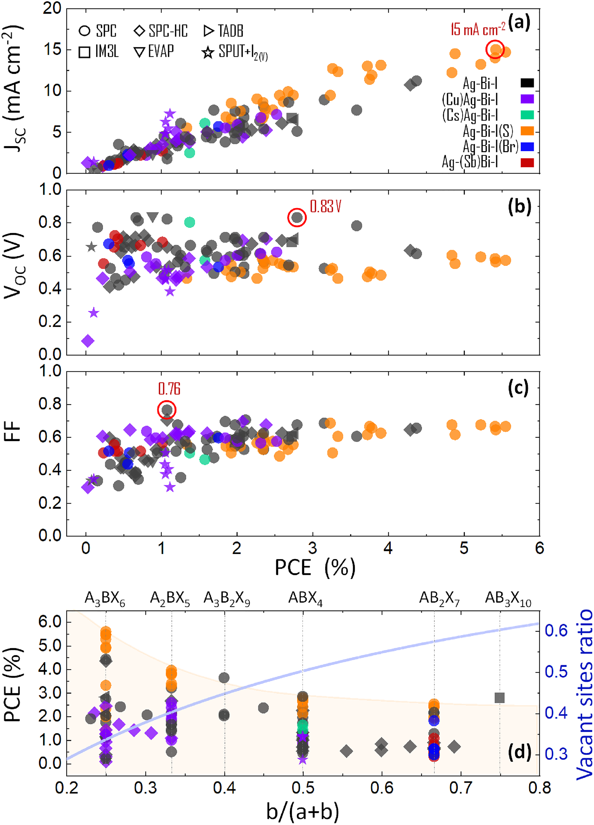
Visualisation of the performance parameters tabulated in Table 4,20–22,26,27,38–40,45,58,59,64–67,75,78,82,88,97–107 showing the correlation between the (a) JSC, (b) VOC, and (c) FF with the PCE. (d) PCE versus nominal stoichiometry expressed as b/(a + b) for A a B b X a + 3b compounds, where A = Ag, Cu; B = Bi, Sb and X = I, Br. Please note that we include the data for Cu–Ag–Bi–I absorbers on this plot by taking b/(b + a) as being the fraction of Bi3+ to the total number of cations in the formula of the species. But we emphasise that these quaternary compounds do not have the general formula A a B b X a + 3b, and the number of vacant sites deviates from the rudorffite structure model (see the ‘Crystal structure of Ag–Bi–I’ and ‘Crystal structure of Cu–Ag–Bi–I’ sections). The blue line in part (d) shows the vacant site ratio in the cation sub-lattice calculated for various stoichiometries.20,21 The shapes of the points correspond to the fabrication methods: SPC (circles), SPC-HC (diamonds), TADB (right-triangles), IM3L (squares), EVAP (down-triangles), SPUT + I2(V) (stars). The colours of the points correspond to various elemental compositions: Ag–Bi–I (black), (Cu)Ag–Bi–I (violet), (Cs)Ag–Bi–I (green), Ag–Bi–I(S) (orange), Ag–Bi–I(Br) (blue) and Ag–(Sb)Bi–I (red). The empty red circles highlight the highest JSC (15 mA cm−2), 75 VOC (0.83 V), 101 and FF (76%) 39 out of all devices reported thus far that we are aware of.
Morphology versus defects
In the early studies of Ag–Bi–I solar cells, there was a tendency to think that the PCE was mainly limited by the poor morphology of the Ag–Bi–I absorber layers. In contrast to hybrid LHPs, Ag–Bi–I semiconductors form adducts with a much higher content of solvent molecules. For example, Ag3BiI6 coordinates with eight DMSO molecules each, 20 which leads to substantial shrinking of the adduct layer upon decomposition during annealing (see Figure 18). This shrinking results in the formation of discontinuous Ag–Bi–I films with columnar morphology. If antisolvent treatment (AST) is used, then crystallisation begins from the top of the film, which results in the formation of voids in the bottom part of the film (see the ‘Defects in Ag–Bi–I compounds’ section for a detailed discussion 56 ). Ghosh et al. 27 optimised the hot casting procedure and improved the morphology of the absorber layers. While they improved the PCE for Ag2BiI5 from 1.6% to 2.6% by changing from spin coating to hot casting, they were not able to exceed earlier reports of Ag–Bi–I solar cells (see Table 4). 27 Similarly, for absorber layers with improved morphology fabricated by co-evaporation of AgI and BiI3, 106 or by co-sputtering of Ag and Bi followed by treatment in iodine vapour, 38 the PCEs reached <1% (Table 4).
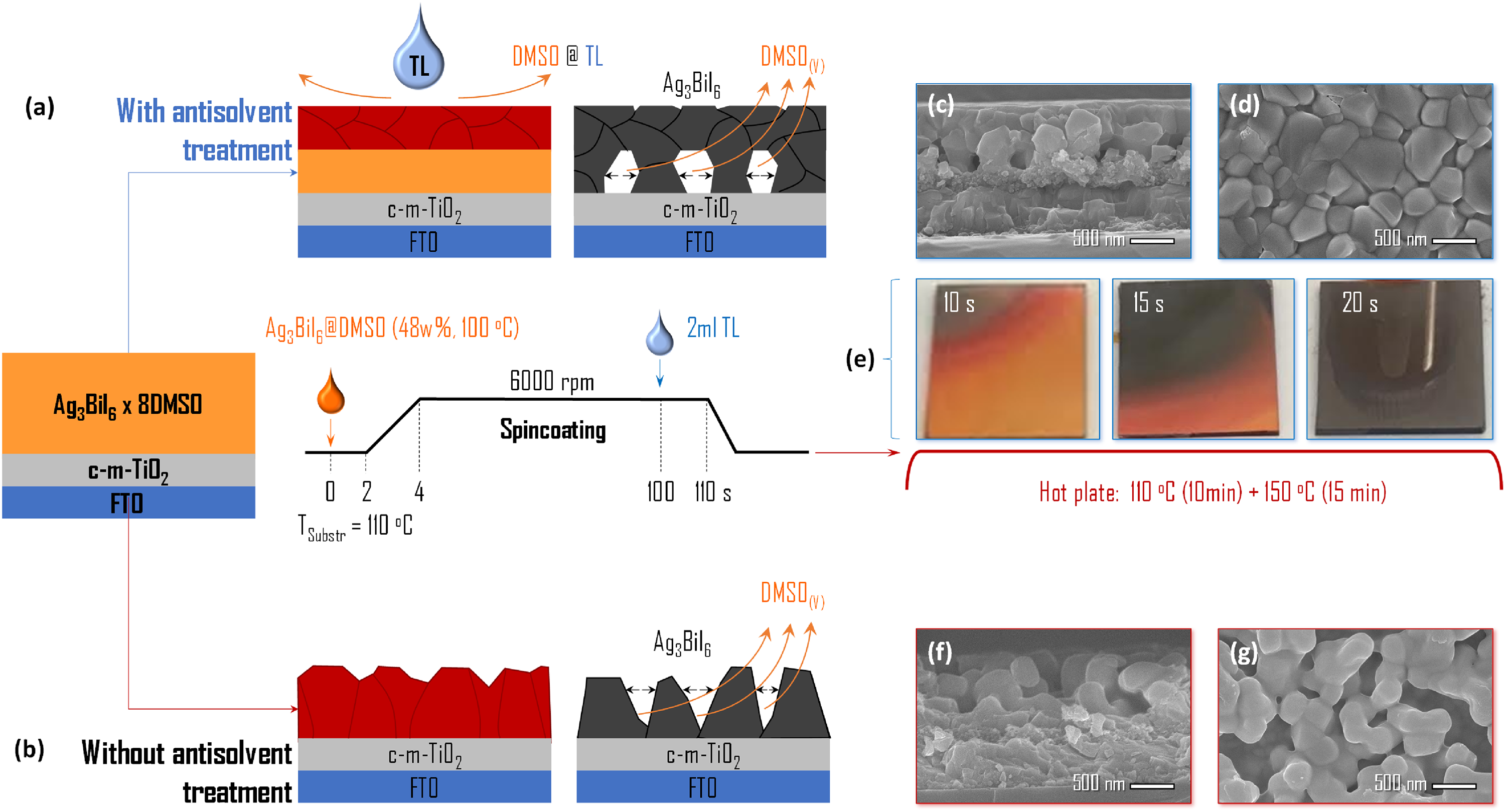
Fabrication of Ag3BiI6 thin films by SPC-HC. Schematic illustration, along with cross-sectional and top-down SEM images of Ag3BiI6 thin films fabricated with (a, c, d) and without (b, f, g) AST with TL. (e) Photographs demonstrating the annealing process of the samples fabricated with AST, resulting in a gradual decomposition of the Ag3BiI6·8DMSO adduct 20 and the formation of smooth mirror-like Ag3BiI6 films. In contrast to the top-down SEM image in part (d) which gives the impression of a compact film, the cross-sectional SEM image in part (c) reveals large holes at the bottom of the film. The samples fabricated without AST (f, g) feature rough, columnar morphology. Reproduced with permission from Turkevych. 108
As we can see in Figure 17(d), the PCE tends to be higher for Ag-rich compositions. Here, we are plotting the PCEs shown for all of the solar cell devices in the above panels (i.e. Figure 17(a) to (c)) as a function of the ratio of Bi3+ to all cation species present in the nominal stoichiometry. We denote this as b/(a + b), which is directly applicable for Ag–Bi–I compounds with the general formula A a B b X a +3b. We emphasise that Cu–Ag–Bi–I quaternary compounds do not have this general formula (see the ‘Crystal structure of Cu–Ag–Bi–I’ section for a description of the structure of these materials). For completeness, it is still useful to include the data for these quaternary absorbers. Interestingly, in Figure 17(d), we observe that the PCEs of solar cells based on Ag–Bi–I absorbers decrease overall as the content of Bi increases. Simultaneously, for increases in b/(a + b), the fraction of octahedral holes in a rudorffite structure occupied by vacancies (i.e. vacant sites ratio) increases (see the ‘Crystal structure of Ag–Bi–I’ section). 20 Thus, we would infer that the probability of lattice defects forming increases as the materials become more Bi-rich, which is consistent with the overall reduction in PCE. This hypothesis correlates with ultrafast transient absorption spectroscopy studies that reveal significantly slower trap-mediated charge-carrier recombination in Ag3BiI6 in contrast to AgBiI4. 109 Also, the time-resolved microwave conductivity figure of merit, studied by Iyoda et al., 110 is significantly higher for Ag-rich compositions. At the same time, we observe no trend in the PCE of solar cells based on Cu–Ag–Bi–I versus b/(a + b) (Figure 17(d)). This may be because these materials are severely underdeveloped in photovoltaics compared to Ag–Bi–I compounds, but also because the fraction of octahedral and tetrahedral holes that are vacant has a more complex relationship with the content of monovalent cations (see the ‘Crystal structure of Cu–Ag–Bi–I’ section).
Nevertheless, we can draw several conclusions: (a) materials within the CuI–AgI–BiI3 phase space are not defect-tolerant semiconductors, (b) trap-mediated charge-carrier recombination seems to be the major performance-limiting factor and (3) Ag–Bi–I compounds that are Ag-rich, in general, give higher PCEs, because they tend to form a lower density of traps. From these arguments, we would suggest three strategies to combat the issue of trap-mediated charge-carrier recombination in Ag–Bi–I photovoltaic devices: (a) improving the crystallinity and minimising the native defect density, (b) compensation of traps by doping and (c) fabrication of extremely thin absorber (ETA) heterojunction structures (as detailed later). This analysis also encourages future efforts on photovoltaics to focus on compounds with lower fractions of the cation sites occupied with vacancies.
Morphology control
Precursor dissolution
Beyond challenges with the formation of pinhole-free Ag–Bi–I thin films, it has also been challenging to find suitable solvents to dissolve the AgI and BiI3 precursors for Ag–Bi–I compounds. BiI3 is sparingly soluble, and AgI is insoluble in polar aprotic solvents commonly used in solution-processing halide compounds, for example, DMF and DMSO.20,22 The strategies employed to overcome this limitation have been to (a) heat the polar aprotic solvents, (b) add a small quantity of acid to the precursor solution to improve solubility, or (c) change to a different solvent system.
In the first case, Turkevych et al. 21 reported that AgI can be dissolved in DMSO when mixed with BiI3 and heated to 110 °C. This was attributed to the formation of [BiI3+x] x – complex ions that facilitate AgI dissolution. 20 The warm solution was deposited by spin coating onto substrates that were not pre-heated (i.e. not hot casting), but with the use of a toluene antisolvent. Pinhole-free Ag3BiI6 thin films were achieved, with 4.3% efficient photovoltaic devices realised (Table 4). 20
In the second case, groups have reported successful dissolution of Ag–Bi–I precursors by adding HI or HCl to the organic solvents. Shao et al. 98 mixed AgI and BiI3 into DMF at a lower temperature of 70 °C, and improved precursor dissolution by adding 50 to 70 µL of 37% HCl to a 1 mL solution. Dense films with large grains were achieved across a range of Ag–Bi–I stoichiometries, however, the photovoltaic performance only reached up to 0.78% for Ag2Bi3I11, mostly due to low short-circuit current densities of up to 2.39 mA cm−2. 98 This was due to low external quantum efficiencies (EQEs) reaching up to 15%. 98 Jung et al. 97 took a different approach of pre-synthesising Ag2BiI5 powders through melt synthesis, then dissolving these powders into a DMF/DMSO solution by adding a small quantity of HI (DMSO:DMF:HI = 3:2:0.2 by volume). However, these Ag2BiI5 films did not completely cover the mesoporous TiO2 substrate, and yet a higher PCE of 2.31% was achieved, mainly due to higher JSC values of 6.33 mA cm−2. 97 A discontinuous morphology was also obtained by Vivo and co-workers with Cu2AgBiI6 thin films. 111 Adding 1.5 vol.% HI to the precursor solution (using a mixture of DMF and DMSO as the solvent) resulted in films that were still discontinuous, but had larger microfeatures with greater coverage of the substrate, leading to an increase in the PCE from 0.60% (no HI) to 1.30% (with HI), and this was attributed to a reduction in the defect density of these films. 111
In the third strategy, groups have investigated the use of primary alkylamines as an alternative to polar aprotic solvents, since the alkylamines are known to dissolve AgI. 22 Kim et al. 22 proposed the use of n-butylamine, and successfully achieved dense thin films that were pinhole-free after annealing at 150 °C. This annealing temperature was found from FTIR measurements to remove remnant n-butylamine and therefore fully crystallise the film. The PCE achieved in photovoltaic devices was 1.22% (see Table 4). 22 Zhu et al. 40 used the same solvent to dissolve AgI and BiI3, and improved the PCE up to 2.1% (see Table 4) by tuning the stoichiometry towards Ag-rich Ag2BiI5, despite the presence of a small number of pinholes.
Similar strategies have been adopted for Cu-based systems. For example, while CuI has low solubility in DMF or DMSO, a combination of CuI and SbI3 was found to dissolve. 96 Similarly, for CuBiI4, the use of HI mixed with N,N-dimethylacetamide successfully dissolved the precursors. 66 However, in both cases, the PCEs reached were poor, below 1%, as is the case with all other solution-processed Cu–Bi–I compounds without Ag added (Table 4). Finally, as discussed earlier in the ‘Particular considerations for the synthesis of quaternary Cu–Ag–Bi–I compounds’ section, adding pyridine to the DMF/DMSO solvent mixture has been found to improve the solubility of the binary iodide precursors for making quaternary Cu–Ag–Bi–I compounds, and this contributed to an improvement in PCE from 0.43% to 1% for Cu2AgBiI6.28,93 However, these PCEs are still low compared to those achieved using hot casting and solvent-free methods (see next the two sections below).
Antisolvent dripping and hot casting
In the solution processing of LHPs, a common strategy to improve film morphology is to employ AST. In this approach, a solvent with poor solubility for the precursors is dripped onto the film during spinning, washing away the original ‘good’ solvent. This induces rapid supersaturation, and the formation of a high density of nuclei, thus increasing the chances of avoiding pinholes (see Dunlap-Shohl et al. 112 for mechanistic details). As mentioned earlier in the ‘Morphology versus defects’ section, AST has been employed with the deposition of Ag–Bi–I and Cu–Ag–Bi–I films, giving rise to improvements in morphology. Since the precursors used are polar, poor solvents will have low dielectric constants and low polarity. The antisolvents that have been investigated are ethyl ether, toluene, chlorobenzene and isopropanol, which all have dielectric constants below 20 (whereas DMF and DMSO have dielectric constants of 37).20,58,78,104 However, the use of antisolvents has not yet proven to be as effective as in LHPs, and poor morphology is often still obtained. Furthermore, stoichiometry, device architecture, and other processing parameters, such as annealing conditions, have had a larger influence than antisolvent dripping on device performance. For example, Zhai et al. 104 compared toluene, chlorobenzene and isopropanol as antisolvents and found isopropanol to give AgBiI4 films with the lowest pinhole density. Although this improved the PCE of AgBiI4 solar cells from 0.64% (without antisolvent) to 1.26% (with isopropanol), 104 the performance falls below that reported by Turkevych et al. 21 for Ag3BiI6 (4.3%) using a toluene antisolvent. 20
The supersaturation during spin coating can also be enhanced through hot casting, in which both the precursor solution and substrate are pre-heated to a certain temperature, and spin coating is carried out while both are warm. This enhances the evaporation rate of the original solvent. Ghosh et al. 27 combined hot casting with antisolvent dripping (using chlorobenzene as the antisolvent), improving the PCE of AgBiI4 from 1.2% (comparable to the best devices reported by Zhai et al. 104 for the same composition) to 2.2% with hot casting. These improvements in device performance were due to increases in grain size and reductions in pinhole density with the use of both hot casting and antisolvent dripping. 27 However, hot casting critically depends on how quickly the substrate and precursor solution are deposited after being taken off from the substrate, and it is difficult to precisely measure the temperature of the solution and substrate during the spin coating process. These factors make hot casting difficult to reliably reproduce in the lab with spin coating, but might be implemented more reproducibly in a manufacturing process where the substrate and precursor temperatures are controlled (e.g. in blade coating).
Overall, in comparing all fabrication methods detailed in Table 4 and visualised in Figure 17(a) to (c), there is no significant difference between spin coating, antisolvent dripping or hot casting. These observations for Ag–Bi–I absorbers also generally apply to Cu–Ag–Bi–I absorbers, although it is more difficult to draw conclusions given the scarcity of reports on these more novel materials. As an illustrative example, Pai et al. 65 reported a champion PCE of 2.45% for solar cells using hot-cast Cu2AgBiI6. Park et al. 58 obtained a slightly higher PCE of 2.53% for Ag2BiI5 with Cu added in, made by conventional spin coating. The stoichiometry and structure of these two absorbers are likely not the same, preventing a direct like-for-like comparison. But, at least we cannot conclude that hot casting leads to a substantial improvement in PCE over conventional spin coating. Furthermore, the effects of annealing conditions on photovoltaic performance are also not clear. More work to understand the process–property–structure–performance relationships of Ag–Bi–I, Cu–Bi–I and Cu–Ag–Bi–I compounds is needed, especially focusing on scalable fabrication methods.
Solvent-free methods
Thermal evaporation of AgBiI4 106 and sputter deposition of Ag3BiI6 and CuBiI4 have been demonstrated,38,67,88 as shown in Table 4. But in all cases, the performance reached has not substantially exceeded those of their solution-processed counterparts, despite dense films being achieved (see Table 4). Khazaee et al. 106 attributed the low performance of the thermally-evaporated AgBiI4 films to be due to the presence of Bi0, found from XPS measurements, which could act as recombination centres. Crovetto et al. 38 synthesised Ag3BiI6 films by first sputter-depositing Ag and Bi, followed by iodisation. A narrow processing window was found to avoid the formation of AgI or BiI3 impurities, and these may have played a role in limiting device performance. Indeed, as discussed earlier on the materials stability of Ag-Bi-I compounds, Ag3BiI6 is thermodynamically favoured to decompose to AgI and BiI3. 56
A similar approach was used to fabricate CuBiI4 films from the vapour phase, in which Cu and Bi were first deposited by sputter deposition, followed by iodisation.67,88 However, it was found that the deposition of a spiro-OMeTAD HTL on top led to the re-dissolution of the dense CuBiI4 film by the 4-tert-butylpyridine and acetonitrile present, leading to a rough morphology with intimate contact between the spiro-OMeTAD and CuBiI4.67,88 This was believed to enhance hole extraction by reducing the required hole transport length, leading to PCEs reaching 1.1%, which slightly exceeded the photovoltaic performance of solution-processed CuBiI4 (0.81%), 66 as seen in Table 4.
Quaternary Cu–Ag–Bi–I films have also been prepared by iodising sputter-deposited metallic Cu/Ag/Bi films (i.e. DMSER). PCEs reaching up to 2.76% have been achieved for DMSER CuAgBi2I8 with a natural CuI layer on top to help facilitate hole extraction. In these devices, a carbon electrode was directly deposited on top of CuI by blade coating and annealing at 100 °C for 10 min. 91 These devices are currently the most efficient for solar cells based on quaternary Cu–Ag–Bi–I absorbers (Table 4).
Further work on developing vapour-based fabrication methods is worthwhile, since these are more easily compatible with large-scale manufacturing than spin coating. Future efforts to improve performance will require detailed analyses of processes causing non-radiative losses, the defects present in the bulk and interfaces of the films, band alignment between the absorber and charge-transport layers, as well as whether the deposition of charge-transport layers onto the absorber damages the film or interface.
Potential of the ETA architecture
As shown in Table 4, the device structures utilised for Ag–Bi–I, Cu–Bi–I and Cu–Ag–Bi–I photovoltaics have mostly been borrowed from those developed for LHPs, that is, using mesoporous TiO2 or SnO2 for the ETL, and an organic HTL over the halide thin film (Figure 19(a)).
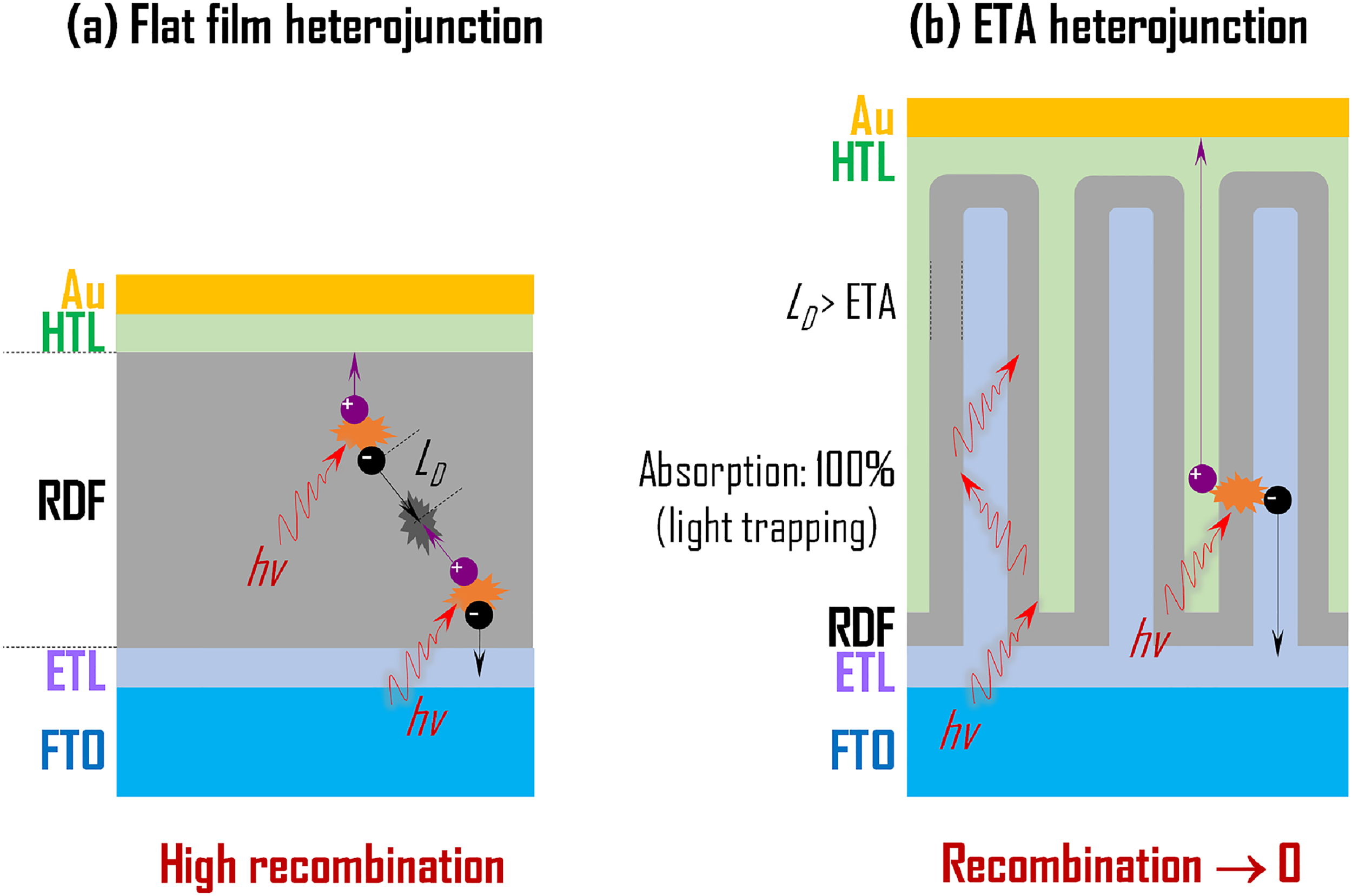
Advantages of the ETA heterojunction structure for Cu–Ag–Bi–I solar cells. The ETA heterojunction structure is an effective approach to alleviate the issue of the short LD and associated high non-radiative recombination rate. In contrast to the flat film heterojunction (a), the absorber layer, which is sandwiched between highly structured ETLs and HTLs in the ETA heterojunction (b), is thinner than the LD, while the trapping of light ensures sufficient light absorption in the thin absorber layer.
In particular, a thick absorber layer is required in this planar or meso-superstructure device architecture. However, Ag–Bi–I (and likely also Cu–Bi–I and Cu–Ag–Bi–I) have shorter diffusion lengths (LD) than LHPs. Rather than using a thick planar thin film, the ETA heterojunction structure could be an effective alternative to alleviate the issue of the short LD. In the ETA heterojunction, the absorber layer is sandwiched between the highly structured ETLs and HTLs (Figure 19(b)). The absorber can therefore be thinner than the LD, while light trapping in the nanostructured device ensures high optical absorption. The ETA structure can therefore significantly improve the collection probability of the photogenerated carriers, because they do not need to travel over large distances before separation. Another important advantage of the ETA structure is more efficient light scattering, which increases the optical path through the device and thereby enhances photon absorption. As a result, the photocurrent of the solar cell can be maximised by a separate optimisation of the optical and electronic thicknesses of the absorber layer. Ag–Bi–I, Cu–Bi–I and Cu–Ag–Bi–I solar cells with the ordered ETA structure have not been realised yet, however, there are several works that demonstrate structured absorbers with a disordered bulk-heterojunction, such as phase separated 0.5Ag3Bi2I9–Cs3Bi2I9, 102 CuBiI4 mixed with doped spiro-OMeTAD or PTB7, 88 and Ag2BiI5 mixed with MWCNT or RGO. 103
Using additives to improve photovoltaic performance
As mentioned earlier, compositional engineering in Ag–Bi–I films has a significant effect on their photovoltaic performance. There have been several works that studied elemental substitutions in Ag–Bi–I compounds with Cs, 78 Sb, 26 Br 59 and S, 75 and a detailed discussion of the effects of doping with these elements is given in the ‘Compositional engineering’ section. In terms of photovoltaic performance, the additive that has led to the highest PCE so far has been S incorporation into Ag-rich rudorffites. These compounds, with a nominal composition of Ag3BiI5.92S0.04, demonstrated a PCE 5.56%, 75 which is currently the record performance amongst all Ag–Bi–I solar cells (Table 4). These increases in PCE were driven by an increase in JSC from 11.2 mA cm−2 for Ag3BiI6 without S incorporation to 14.7 mA cm−2 with 4% S incorporation (Table 4). 75 As can be seen from Figure 17(a), these were among the highest JSCs reported for the Ag–Bi–I system. The increase in JSC was due to an increase in the EQE, as well as a reduction in the optical bandgap from 1.87 eV (no S) to 1.82 eV (4 at.% S), which enhanced light absorption. As discussed in the ‘Compositional engineering’ section, the reduction in bandgap came about from the VBM being raised. Further increases in S incorporation reduced the bandgap more, but were accompanied by further decreases in the VOC (see Table 4). Pai et al. 75 attributed these reductions in VOC to an increase in the density of recombination centres.
Device stability
Several groups have reported stable performance of unencapsulated Ag–Bi–I photovoltaics when stored in ambient air, dry air, or in an N2-filled glovebox.22,26,40,45,59,67,75,78,97,101,107 A range of stability tests have been conducted, from 10 days 22 to 77 days 59 in ambient air. In these tests, the devices were stored in the designated testing environment, and measured under 1 sun illumination at regular time intervals. In most cases, only a very small decrease in PCE was observed, on the order of 5% to 15%.22,45,75 In the case of AgBi2I7 doped with 10% Br, a slight improvement in PCE was observed after storing in ambient air in the dark for 77 days, and this was attributed to changes in the TQ1 HTL (see footnote of Table 4 for full name) after oxygen exposure, since the increase in PCE correlated with an increase in JSC. 59 In addition, Lu et al. 45 found that AgBiI4 demonstrated greater thermal and photostability than MAPbI3 perovskite. In thermogravimetric analysis measurements, the onset in mass loss for AgBiI4 was 260 °C (due to BiI3 sublimation), whereas the onset temperature for the perovskite was 200 °C (due to methylammonium iodide removal). 45 When pristine films were sealed in an inert gas environment and exposed to 1 sun illumination for up to 3 h, AgBiI4 showed no phase degradation, whereas the perovskite formed a PbI2 impurity peak after only 1 h. 45
However, it will be important to also understand long-term changes in PCE under continuous operation at the maximum power point. Zhang et al. 101 found that although the PCE decreased by <5% after repeated measurements over a period of 500 h in air, under continuous operation, the PCE decreased by approximately 40% under continuous operation for 50 s. These changes may arise from heat-induced, ion migration or changes to the device at the interfaces during operation, and should be investigated further. Indeed, as discussed earlier in the ‘Defects in Ag–Bi–I compounds’ section (on the effects of AgI impurities) and in the ‘Ion migration in Ag–Bi–I’ section (on ion migration), ionic species can be released and migrate to the top metal electrode, causing corrosion and performance degradation. 56 This occurs even for metal electrodes that would normally be considered inert, such as Au, and motivates further work to understand the mechanisms involved, as well as mitigation strategies (e.g. developing more inert electrodes). Achieving stable operation at the maximum power point and under continuous illumination will be important for Ag–Bi–I photovoltaics to ultimately pass standard accelerated degradation tests.113,114
In summary, from Table 4 and Figure 17, we can see that reasonably high parameters of 15 mA cm−2 for JSC, 75 0.83 V for VOC, 101 and 76% for FF 39 have been demonstrated in different devices. This suggests that a properly optimised device can potentially demonstrate a PCE of around 10%. We can suggest that the next generation of these halide absorber solar cells should adopt Ag- or Cu-rich compositions for absorber layers with heterovalent doping and the ETA heterojunction device structure.
Indoor light harvesting
IPVs are gaining increasing attention as a highly promising route to sustainably powering Internet of Things (IoT) devices.24,115 The IoT is an ecosystem of interconnected devices that can communicate with each other via the cloud. Such an ecosystem is considered to embed ‘intelligence’ into infrastructure, by making them responsive and adaptable (i.e. smart homes, smart factories, smart agriculture, etc.). The IoT is predicted to substantially improve quality of life, increase productivity and reduce CO2eq emissions by making processes more efficient.24,115–118 As the IoT ecosystem increases in size towards the trillion-node level, a critical question is how these autonomous devices can be sustainably powered. Currently, there is a heavy reliance on batteries, which have limited lifespan, and this could not only restrict the size and number of applications of the IoT, but also lead to substantial waste. 24 In this context, harvesting ambient light as a power source for IoT devices is highly appealing. IPVs can be integrated into the IoT node (Figure 20(a)), and could either directly power the IoT device (harvest-use), or both power the IoT device and recharge an energy storage device (e.g. battery or supercapacitor) that then powers the device in the dark (Figure 20(b), harvest-store-use). IPVs are advantageous over other energy harvesters because ambient light is a reliable source of energy that is widely available, and there is no need for the IPVs to be directly in contact with the light source. Furthermore, the energy density of indoor light sources is high compared to other sources of energy, typically up to 300 to 350 µW cm−2 under 1000 lux illuminance. Figure 20(c) illustrates that the instantaneous power IPVs can harvest under direct illumination is sufficient for a wide range of low-power communications protocols commonly used for wireless sensors 115 with a relatively compact area of 10 cm2. The excess energy can be stored to power the IoT node in the dark. Given the highly predictable availability of ambient lighting, the power management system and total power harvested by the IPV can be designed for. As such, the IPV industry is one of the fastest-growing photovoltaic markets. 115
Motivation for using Ag–Bi–I for IPVs. (a) Schematic of an RFID tag with an IPV. Reproduced with permission from Mathews et al. 116 Copyright 2019, Wiley. (b) Illustration of IoT nodes based on the ‘harvest-use’ and ‘harvest-store-use’ concepts. 24 (c) Power produced by IPV over a range of PCEs under different illuminances. A total of 1000 lux illuminance is taken to have 350 µW cm−2 irradiance. Power consumption of communication protocols from Mathews et al. 115 (d) Radiative limit and i-SLMEs under WLED and FL light sources. Reproduced under the terms of the CC-BY license from Pecunia et al. 24 Copyright 2021, The Authors.
Cu–Ag–Bi–I materials can have an important impact on the IPV field. Commercial IPVs are dominated by hydrogenated amorphous silicon (a-Si:H). However, owing to the high defect density in a-Si:H, the PCEs are limited up to 21%, 119 and are mostly in the 4.4% to 9.2% range.120,121 Higher PCEs under indoor light sources have been achieved by organic photovoltaics (to 30.3%), 122 dye-sensitised solar cells (DSSCs; to 34.0%, Table 5) 117 and LHP photovoltaics (to 41.2%, Table 5). 124 However, organic IPVs are limited by high synthesis costs, especially for the complex molecules used in the most efficient devices. 127 LHPs are limited by the presence of toxic and bioaccumulative Pb in a readily accessible form and may be prevented by legislation (e.g. EU restriction of hazardous substances directive) for use in consumer electronics. 128 Furthermore, LHPs, organic PV and DSSCs are commonly processed using large quantities of toxic solvents (e.g. DMF or chlorobenzene). 12 Simple inorganic compounds that can be processed using low thermal budget methods using low-toxicity solvents (e.g. DMSO 12 ) or solvent-free are therefore highly appealing. Hoye, Pecunia, and co-workers. 24 calculated the efficiency limit expected based on the measured optical absorption spectra (i.e. indoor spectroscopic limited maximum efficiency (i-SLME)) for a range of inorganic PIMs and found that Ag3BiI6 had a radiative limit and i-SLMEs reaching up to 56.2% under 1000 lux white light-emitting diode (WLED) illumination for Ag3BiI6 (Figure 20(d)). 23 The high i-SLMEs were due to the Ag–Bi–I compound having an optimal bandgap (close to 1.9 eV) for harvesting visible indoor lighting (WLED or FL), as well as its high absorption coefficients (see Figure 6). 38 These factors, coupled with the ability to synthesise Ag–Bi–I semiconductors using a small number of steps (compared to organic molecules), and compatibility with processing by nontoxic solvents or solvent-free methods, make the class of materials promising.
Performance of Ag–Bi–I and Cu–Ag–Bi–I IPVs. The average value and uncertainty for each parameter are shown, along with the value of the champion device in brackets, where all of this information is available. Otherwise, the champion performance reported is shown. The light source used in these reports was WLEDs, except for the report showing DSSCs, which were measured under FL lighting. Please note that not all devices were measured under the same illumination conditions, and the standards for indoor photovoltaic measurements had not been published when these reports were made. 1
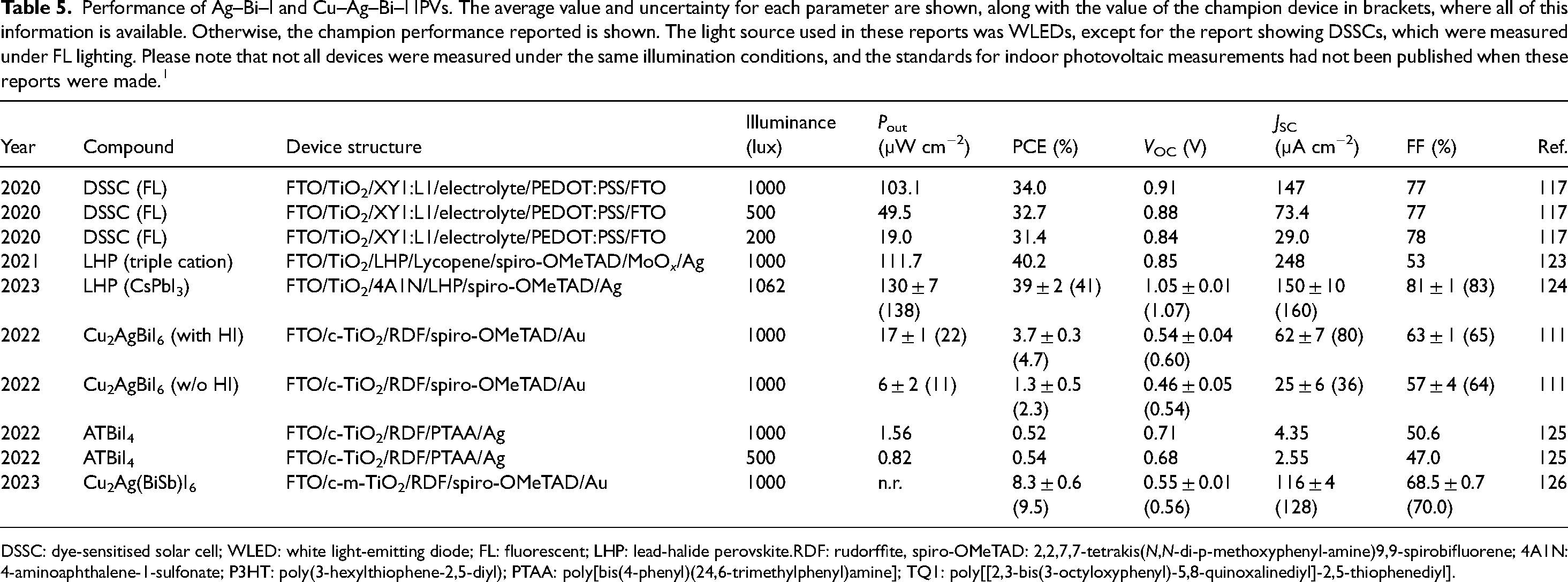
DSSC: dye-sensitised solar cell; WLED: white light-emitting diode; FL: fluorescent; LHP: lead-halide perovskite.RDF: rudorffite, spiro-OMeTAD: 2,2,7,7-tetrakis(N,N-di-p-methoxyphenyl-amine)9,9-spirobifluorene; 4A1N: 4-aminoaphthalene-1-sulfonate; P3HT: poly(3-hexylthiophene-2,5-diyl); PTAA: poly[bis(4-phenyl)(24,6-trimethylphenyl)amine]; TQ1: poly[[2,3-bis(3-octyloxyphenyl)-5,8-quinoxalinediyl]-2,5-thiophenediyl].
The demonstration of high i-SLMEs for Ag3BiI6 was only made in 2021. 23 Since then, Turkevych et al., 46 Grandhi et al., 111 and Arivazhagan et al. 125 have reported initial findings on Cu–Ag–Bi–I IPVs. The compounds explored were AgBiI4, Cu2AgBiI6 and ATBiI4, respectively, where AT = 2-aminothiazolium. The molecular structure of AT, along with the crystal structure of ATBiI4, is shown inset in Figure 21(a) (see the ‘Structure–property relationships of compounds in the CuI–AgI–BiI3 phase space, and their derivatives’ section for the crystal structure of AgBiI4 and Cu2AgBiI6). Unlike the all-inorganic compounds, the large size of AT results in a one-dimensional structure, comprised of edge-sharing chains of BiI6 octahedra. 129
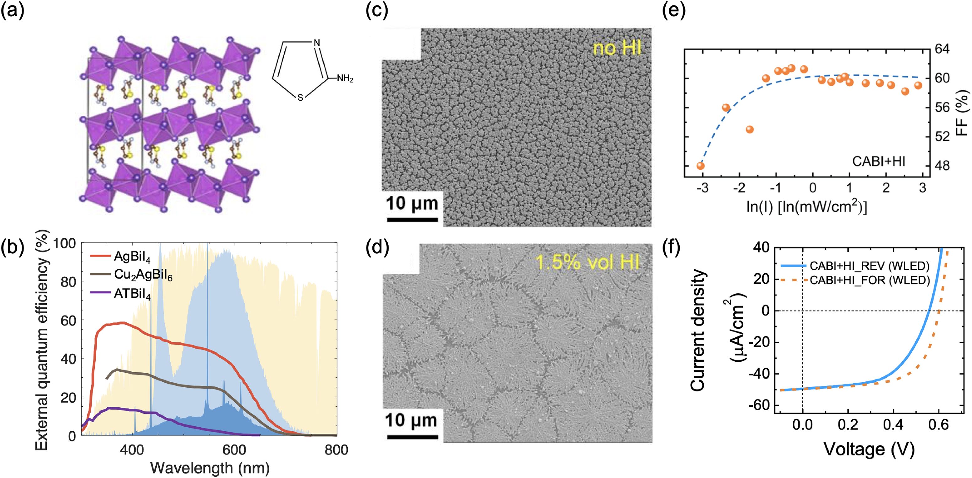
Performance of recently reported Ag–Bi–I and Cu–Ag–Bi–I IPVs. (a) Crystal structure of ATBiI4, with the structure of AT (inset). Reproduced under the terms of the CC-BY license from Arivazhagan et al. 125 Copyright 2022, The Authors. (b) EQE against wavelength of incident light for AgBiI4, 46 Cu2AgBiI6 111 and ATBiI4 IPVs, compared to the spectra for WLED (light blue), FL (dark blue) light sources, as well as 1 sun (yellow). Morphology of Cu2AgBiI6 (c) without and (d) with 1.5% HI added to the precursor solution. (e) Fill factor of Cu2AgBiI6 IPVs under 100–45,000 lux illuminance. (f) Forward and reverse sweeps for Cu2AgBiI6 IPVs. Parts (c) to (f) are reproduced under the terms of the CC-BY license from Grandhi et al. 111 Copyright 2022, The Authors.
The EQE spectra from the three compounds are shown in Figure 21(b). All three materials have bandgaps in the range of 1.78 to 1.96 eV,46,111,125 and the EQE onset for these devices was from approximately 700 nm wavelength, with an inflection point close to the optical bandgap. In the case of Cu2AgBiI6, the authors reported a four-fold increase in PCE under WLED lighting compared to 1 sun illumination, due to the better spectral match of their devices to indoor lighting. 111 Importantly, the VOC under 1000 lux illuminance remained relatively close to the VOC under 1 sun illumination (0.60 V vs. 0.70 V, respectively). 111 The ATBiI4 devices exhibited lower EQEs and lower device performance (Table 5), which may be due to discontinuities in the film and possibly BiI3 impurities. High trap densities on the order of 1018 cm−3 were also found from space-charge limited current densities measurements, and this would also limit performance. 125
Challenges with morphology and phase impurities were found to limit the efficiency of Cu2AgBiI6 IPVs. An SEM image of Cu2AgBiI6 films is shown in Figure 21(c). Attempts were made to improve this morphology by adding small quantities of HI to the precursor solution. While this led to larger domains (Figure 21(d)), discontinuities in the film remained. Intensity-dependent measurements showed that the FF decreased at low illuminances (Figure 21(e)), and this was attributed to the effects of morphology leading to dark currents that play a more substantial role under indoor lighting, given the low photocurrents at low illuminances. Furthermore, intensity-dependent VOC measurements showed that the diode ideality factor increased from 1.2 (0.1–1 sun) to 1.6 (100–45 000 lux), suggesting that under lower illuminances, non-radiative recombination due to bulk defects played a greater role. Indeed, phase impurities were found from XRD and PL measurements, and some of these could have acted as recombination centres. 111 Very recently, the same group reported an improvement in the morphology, along with a reduction in defect density, by alloying a small quantity of Sb into the pnictogen site. This led to an improvement in the PCE under 1000 lux from 5.52% to 9.53%, mainly due to an increase in the JSC from 72 to 128 µA cm−2. 126
Across all Cu–Ag–Bi–I IPVs reported thus far, hysteresis was found in the photovoltaic performance (Figure 21(f)). All three groups used a similar device architecture (refer to Table 5) to that commonly used for LHPs, from which hysteresis is commonly reported. Thus, in addition to efforts to suppress ion migration, it may also be important to investigate alternative electron/HTLs that could reduce hysteresis effects through interface passivation or by inhibiting ionic motion. 130 Furthermore, Al-Anesi et al. 126 reported a reduction in the hysteresis of Cs2AgBiI6 at high illuminance through Sb alloying, which may be due to a reduction in defect density.
Thus, there have already been encouraging initial results on Cu–Ag–Bi–I IPVs, with PCEs reaching into the range of commercial-standard a-Si:H IPVs, and are at a comparable level to initial BiOI and vacancy-ordered triple perovskite PIM IPVs. 23 This sets the stage for future efforts at improving the morphology, optoelectronic quality, and device structure to bring Cu–Ag–Bi–I towards their potential as IPVs.
Photodetectors
Photodetectors have important applications in medical imaging, surveillance cameras, machine vision, optical communications, and many more (Figure 22(a)). 131 While crystalline inorganic semiconductors (such as Si or InGaAs) are well established in commercial photodetectors, with high detectivity >1011 Jones, rapid advances in new applications call for innovations in imaging technology. 131 Solution-processed thin film semiconductors are particularly appealing for many reasons. They can be directly incorporated into read-out integrated circuits, which circumvents the cumbersome integration of conventional semiconductors, allowing greater miniaturisation. Solution-processed semiconductors are also compatible with large-area manufacturing techniques, such as roll-to-roll processing, spray coating, doctor blading or inkjet printing. 133 Furthermore, solution-processed thin films can be integrated with flexible substrates, which is important for wearable electronics, or integration into IoT sensor nodes. 134 Thus, chalcogenide colloidal quantum dots (QDs), organic materials and LHPs have gained significant attention as novel photodetector materials, and in some cases, detectivities have exceeded those of Si-based photodetectors in the visible wavelength range. 131 Cu–Ag–Bi–I materials are worth investigating for photodetection, because of their lower toxicity compared to Cd- or Pb-based colloidal QDs and LHPs, and their potentially simpler fabrication process compared to organic materials. Up to now, Ag–Bi–I and Cu–Bi–I compounds, as well as Ag/Cu alloys, have been investigated (Table 6), covering the UV and visible (UV–VIS) wavelength ranges (Figure 22(a)).
Application of Cu–Ag–Bi–I materials in solution-processed photodetectors. (a) Application of photodetectors at different wavelengths, 131 and the wavelengths of Cu–Ag–Bi–I photodetectors have been demonstrated thus far. Please note that Ag–Bi–I X-ray detectors have also been demonstrated, as elaborated on in the ‘Broader potential applications’ section. Illustration of photodetectors made in the (b) PC and (c) PD structure, as reported for Cu–Ag–Bi–I absorbers. (d) Comparison of the spectral responsivity reported in Pecunia et al. 41 for Ag2BiI5 and in Zhang et al. 93 for Cu2AgBiI6. Rise and fall in photocurrents under chopped illumination for (e) AgBi2I7 nanocrystal (under AM 1.5G illumination) and (f) Cu2AgBiI6 (under 405 nm wavelength illumination) PDs. Part (e) reproduced with permission from Premkumar et al. 132 Copyright 2020, American Chemical Society. Part (f) reproduced with permission from Zhang et al. 93 Copyright 2022, American Chemical Society.
Champion reported performance of halide Cu–Ag–Bi–I for photodetectors. The spectral response noted refers to the spectra the photodetectors were tested under, and not to the full range of spectra the devices could in principle work under (UV and Vis in all cases).
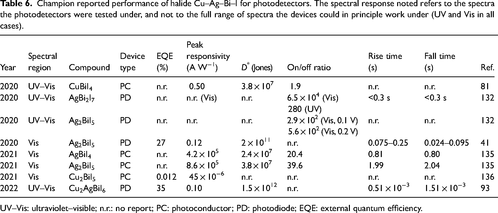
UV–Vis: ultraviolet–visible; n.r.: no report; PC: photoconductor; PD: photodiode; EQE: external quantum efficiency.
Thus far, groups developing Cu–Ag–Bi–I photodetectors have adopted either a lateral photoconductor (PC) structure (Figure 22(b)) or a vertical photodiode (PD) structure (Figure 22(c)), as shown in Table 6. The PC structure is simpler and involves depositing identical metal electrodes onto the Cu–Ag–Bi–I. The increase in conductivity following light absorption is read by applying an external voltage. In the case of Cu–Ag–Bi–I, the PD structures adopted have been identical to the architectures used in photovoltaics, although the thicknesses and processing of the individual layers are often different between these two applications because of the different ways in which they operate. In PDs, the built-in potential assists with the extraction of the photogenerated charge carriers, and this is often further assisted by the application of an external bias. 131
The key performance metrics for photodetectors are related to their efficiency, noise and speed. Efficiency includes the EQE, responsivity and specific detectivity. The responsivity (R) is the ratio of the current extracted to the optical power input and can be calculated from the EQE (ηEQE) from equation (1), where hν is the photon energy and q is the fundamental charge.
Ultimately, the overall figure of merit for the sensitivity of photodetectors is the specific detectivity (D*), which can be calculated from R, the noise current (IN), the noise bandwidth (B) used in measuring the noise current, and detector active area (A) from Equation 2.
Noise is the random fluctuation in the output current, and is often due to frequency-dependent flicker (1/f) noise (due to trapping in the bulk or surface) or frequency-independent thermal noise (due to the random thermal motion of charge carriers) and dark shot noise (due to dark current).
137
Often, in calculating D*, groups would consider IN to be solely due to the dark shot noise, but this would often lead to an overestimation of D*, since many other sources of noise also play a role. For example, for Ag2BiI5 PDs, the D* would have been 2 × 10¹² Jones if only shot noise was considered. But after considering thermal noise as well as shot noise, the D* reduced by an order of magnitude to 2 × 10¹¹ Jones.
41
To account for all sources of noise and accurately determine D*, the noise current as a function of frequency should be directly measured. However, the specific detectivities reported by all other groups in Table 6 were calculated based only on the dark current noise.81,93,135,136
Finally, the speed of the photodetector is commonly characterised by its response time, which is usually defined by the time for the photocurrent to increase from 10% to 90% of the maximum photocurrent under chopped illumination (rise time), or decrease from 90% to 10% (fall time).93,131 Another metric for the speed of photodetectors is the maximum frequency they can operate at (i.e., the cut-off frequency). 131 However, this parameter has not yet been reported for Cu–Ag–Bi–I photodetectors.
A comparison of the responsivity of recently reported Cu–Ag–Bi–I PD is shown in Figure 22(d), showing the ability of these devices to operate over a wide spectral range from UV to visible. Higher responsivity values reaching 0.5 A W−1 were reported for CuBiI4 PCs under AM 1.5G illumination (100 mW cm−2) by Qu et al. 81 These PCs were made in a lateral configuration, in which both Au electrodes were deposited onto the front surface of the CuBiI4 film. This was important to achieve rectification with an on/off ratio of 1.9, since pinholes were present in the morphology of the films, 81 and a high leakage current may have occurred if a vertical device structure were used.
Much higher responsivities on the order of 105 A W−1 were reported for AgBiI4 and Ag2BiI5 PCs by Prasad et al. 135 The films had a more compact morphology than the CuBiI4 films made by Qu et al., 81 and the key to achieving this was a post-annealing process at 125 °C for 15 min, which reduced the density of pinholes and increased the size of grains. 135 The responsivity was calculated from the ratio of the photocurrent to incident power, measured under 454, 532 and 633 nm wavelength excitations at a power density of 0.1 mW cm−2 and 1 V bias. 135 However, these responsivities significantly exceed the ideal responsivities (when EQE is 100%), which are <1 A W−1 at these excitation wavelengths. A possible explanation for this is photoconductive gain, in which the accumulation of majority charge carriers can lead to measured EQEs exceeding 100%. 138
An advantage of the PD structure over the PC structure is that a built-in field is already present without any external bias applied. PDs are therefore capable of being self-powered, which is important for low-power applications, such as in sensor nodes for the IoTs.24,41 Zhang et al. 93 reported self-powered Cu2AgBiI6 PD, which had a responsivity of 0.085 A W−1 under 405 nm wavelength excitation. The spectrally resolved responsivity over the UV and visible wavelengths is shown in Figure 22(d), from which it can be seen that improved performance was obtained using P3HT as the HTL rather than spiro-OMeTAD. This was because devices with P3HT had a higher JSC. Zhang et al. 93 also found that passivating the surface of the Cu2AgBiI6 films with phenethylammonium iodide (PEAI) led to an increase in the built-in potential, and this improved the photocurrents obtained.
A photoresponse further into the UV was obtained from AgBiI4, Ag2BiI5 and AgBi2I7 QDs by Premkumar et al., 132 with an average size of 5 nm. These QDs were found to have stronger excitonic characteristics and blue-shifted absorption compared to bulk films, with the excitonic peaks of AgBiI4, Ag2BiI5 and AgBi2I7 occurring at 2.99, 3.04 and 2.91 eV, respectively. 132 These QDs were used in PDs, with the device structure: FTO/nc-TiO2/QD/MoO3/Al, in which the nc-TiO2 layer was a film comprised of 50 nm sized nanocrystals. The photocurrent at 0.1 and 0.2 V applied bias was measured under 1 sun illumination, and the highest on/off ratios were reached for the AgBi2I7 PD, with a value of 6.5 × 10⁴ (Table 6). The AgBi2I7 PD also exhibited the best performance as a UV detector (under 390 nm wavelength excitation), with an on/off ratio of 280 and responsivity of 0.15 A W−1. In these UV detectors, the MoO3 layer was removed. Under both 1 sun and UV illumination, all devices had a long rise time <0.3 s, with a sawtooth pattern in the photocurrent under chopped illumination (Figure 22(e)), and this was attributed to unrelaxed electrons in excited state energy levels. 132 Prasad et al. 135 reported longer response times for AgBiI4 and Ag2BiI5 thin film PDs, on the order of 0.8 s (AgBiI4) and 2 s (Ag2BiI5). By contrast, much shorter response times on the order of milliseconds were reported by Zhang et al. 93 for Cu2AgBiI6 (Figure 22(f)).
An important advantage widely reported for Cu–Ag–Bi–I photodetectors is their stability under ambient environments. For CuBiI4, Cu2AgBiI6, as well as the Ag–Bi–I QDs from Premkumar et al., 132 the photocurrent under chopped illumination was measured for 100–500 s, and in all cases no decrease in performance was found.81,93 Prasad et al. 135 kept their AgBiI4 and Ag2BiI5 PDs in ambient air for 15 days and found no significant change in current–voltage curves. As another example, Shaji and co-workers found that Cu2BiI5 photodetectors remained operational after storage for 30 days in ambient air, with photocurrents that were similar to or less than an order of magnitude smaller than fresh devices. 136
Thus, Cu–Ag-Bi–I are potential solution-processable semiconductors for next-generation photodetectors, with promising stabilities in air. The development of these materials into photodetectors is still at an early stage and warrants further development, particularly in improving the processing and device architecture to further improve the performance. It will also be important to measure the noise current of these devices to more accurately calculate the specific detectivity, and elucidate in more detail the factors influencing the response time of these devices.
Broader potential applications
A core advantage of Bi–I-based materials is the high atomic number of these elements, which is important for efficiently attenuating ionising radiation. 139 Ionising radiation is widely used for non-invasive diagnostics, such as in security screening, detection of radionuclides from nuclear waste, or medical imaging. Across all applications, detectors with higher sensitivity, and the ability to detect lower dose rates (i.e. lower limit of detection (LoD)) are desired. For example, in medical imaging, the standard dose rate is 5500 nGyair s−1, which is four orders of magnitude above background levels of ionising radiation, thus posing a risk to the patient during medical scans.139,140 Achieving detectors that can directly convert X-ray photons to electrical signals with lower LoD and higher sensitivity requires materials with high average atomic numbers (Zav) and density, since the linear attenuation coefficient is proportional to ρZav4.30,139,140 AgBi2I7 was recently investigated for X-ray detection and was found to have linear attenuation coefficients (Figure 23(a)) over an order of magnitude larger than amorphous selenium (α-Se), which is the industry-standard material for direct-conversion detectors in medical imaging.30,139 This is particularly advantageous for detecting higher-energy X-rays. For example, Tie et al. 30 showed that whilst several millimetres thick α-Se would be needed to attenuate 100 keV X-rays, only 0.5 mm of AgBi2I7 would be needed. Furthermore, AgBi2I7 single crystals were found to have electron/hole mobilities on the order of hundreds of cm2 V−1 s−1, with mobility-lifetime (µτ) products on the order of 10−3 cm2 V−1 for both electrons and holes. 30 X-ray detectors were made with a PC structure (Figure 23(b), inset), in which the AgBi2I7 single crystal was sandwiched between two parallel Au electrodes. The photocurrent was measured from 11,403 nGyair s−1 down to 105 nGyair s−1 (Figure 23(b)) from a 60 kVp W-target anode X-ray tube, with 43 keV mean photon energy. From these measurements, the LoD was found to be 72 nGyair s−1 by extrapolating the signal-to-noise ratio down to 3, as shown in the inset of Figure 23(b). 30 This is a substantial improvement over the current medical standard, and the sensitivity obtained (282.5 µC Gyair−1 cm−2) exceeded that of α-Se (20 µC Gyair−1 cm−2). 30 These AgBi2I7 X-ray detectors also had higher sensitivities than the first report of Cs2AgBiBr6 double perovskite X-ray detectors (105 µC Gyair−1 cm−2), 140 but fall short of current state-of-the-art values for LHPs (now exceeding 104 µC Gyair−1 cm−2). 139 Lead-halide perovskite X-ray detectors have also achieved directly measured LoD values below 40 nGyair s−1. 35 Shaon et al. 47 theoretically analysed AgBi2I7 radiation detectors, and found that these devices have a predicted upper limit in sensitivity of 313 µC Gyair−1 cm−2 at 20 keV (for mammography), and 2870 µC Gyair−1 cm−2 at 60 keV (for chest radiography). It should be noted that the calculated upper limit in sensitivity of LHPs is only 8000 µC Gyair−1 cm−2 yet sensitivities exceeding this have been reported, which may be due to multiplication effects, such as photoconductive gain. 141 Thus, there is scope for further improvements in the performance of AgBi2I7 radiation detectors, and it will be important to determine and control the photoconductive gain (such as by controlling the device architecture), as well as understand the role of ion migration in these devices.
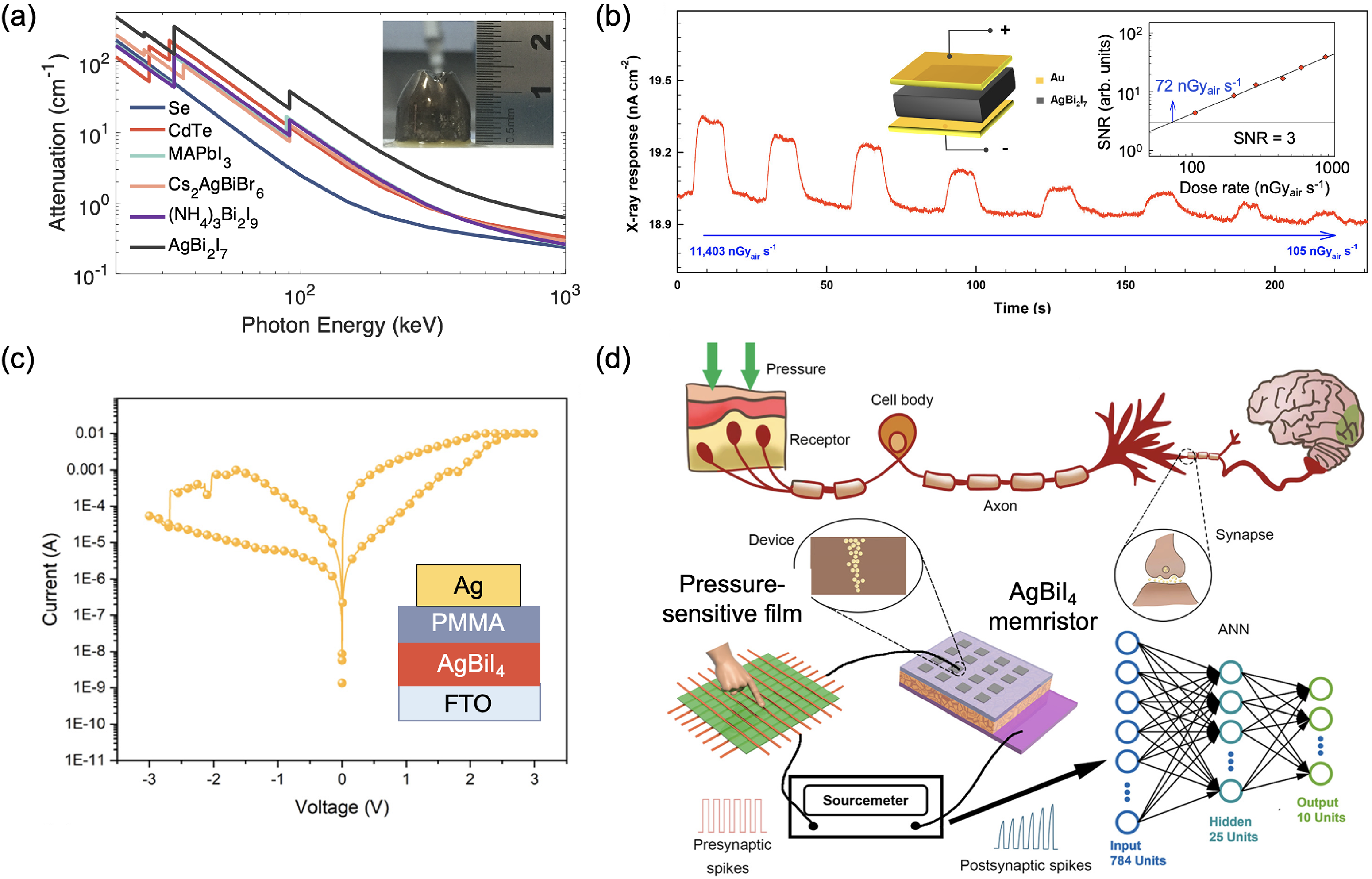
Broader applications of Ag–Bi–I in X-ray detectors and artificial synapses. (a) Attenuation coefficient of AgBi2I7 for ionising radiation, with a photograph of the AgBi2I7 single crystal inset. (b) Photocurrent of AgBi2I7 single crystal PCs with different dose rates of X-rays. Inset is a schematic of the PC, as well as the determination of the lowest detectable dose rate from the SNR. Part (b) and inset to part (a) reproduced with permission from Tie et al. 30 Copyright 2020, American Chemical Society. (c) Typical resistive switching curve for AgBiI4 memristors, with the device structure inset. (d) Illustration of how humans respond to tactile signals (top), and the replication of this system using a pressure-sensitive film and AgBiI4 memristors. Parts (c) and (d) reproduced with minor adaptations from Ye et al. 31 under the terms of the CC-BY-NC 3.0 license. Copyright 2022, The Authors.
Beyond photo-active applications, AgBiI4 has also exhibited resistive switching.31,142 Recently, there has been a surge of interest in developing novel materials for resistive switching random access memory (ReRAM) devices that could achieve high integration density, overcome the scaling limitations of Si flash memory, and be compatible with polymer substrates for flexible memristors. 142 Ye et al. 142 achieved compact AgBiI4 films at a low processing temperature of 150°C through dynamic hot casting, in which chlorobenzene was used as the antisolvent. These films were integrated into a vertically structured device, with a transparent conducting oxide (ITO 142 or FTO 31 ) on the bottom electrode, and Ag as the top electrode (Figure 23(c)). A thin layer of poly(methyl methacrylate) (PMMA) was used between the AgBiI4 and Ag electrode to prevent the degradation of the AgBiI4 layer by reactions with Ag. These devices exhibited low set and reset voltages of 0.16 and −0.16 V, respectively, with an on/off ratio exceeding 104. 142 The on/off ratio is comparable with the highest reported for LHPs, and the set/reset voltage significantly lower, which is important for achieving ReRAM with low-power consumption. These devices exhibited excellent data retention, maintaining the resistivity in the high and low resistance states for up to 104 s (at a reading bias of 0.02 V). The endurance of the devices was also high, maintaining the resistive switching behaviour after cycling 700 times. When built on flexible substrates, the AgBiI4 exhibited inferior performance, with an on/off ratio on the order of 102, but this was durable after 1000 bending cycles, demonstrating the mechanical robustness of these devices. 142
The proposed mechanism for resistive switching in the AgBiI4 memristors was the formation of conducting Ag-based filaments. Although the PMMA layer prevented reactions between the AgBiI4 and Ag, it was thin enough for Ag+ cations to diffuse through to form these filaments. 142 However, in a later report, the same group increased the thickness of AgBiI4 from 500 nm to almost 1 µm, which led to higher set/reset voltages (Figure 23(c)). 31 The mechanism was proposed to be different for the thicker devices due to the reduction in the electric field with an increase in layer thickness, to the extent that it was insufficient to cause Ag filament formation. Rather, the resistive switching mechanism was proposed to be based on VI defects. 31 These thicker devices exhibited a continuous reduction in resistivity during the set process (at 1.5 V) and an increase in resistivity during the reset process (at −1.5 V), which resembles the behaviour of biological synapses. This led to the construction of an artificial sensor neural system based on a pressure-sensitive film and AgBiI4 memristor artificial synapse feeding information to an artificial neural network that replicates the human tactile sensing system, as illustrated in Figure 23(d). 31 Ag–Bi–I semiconductors are therefore highly promising for neuromorphic computing.
Finally, an area that has not yet been explored is the application of Cu–Ag–Bi–I materials for photocatalysis or photoelectrochemical cells. As shown in Figure 24, the band positions of Ag–Bi–I and Cu–Bi–I compounds are suitable for proton reduction to form H2, CO2 reduction, or water oxidation to form O2 gas. Stable materials for clean solar fuel production are urgently required, and the device structures developed for photovoltaics can be beneficial for improving the performance and stability of these materials for photocathodes or photoanodes. 9 Furthermore, a bandgap of approximately 2 eV is optimal for single-junction devices for solar-driven water splitting (i.e. for both water oxidation and reduction), with an efficiency limit estimated to be in the range of 15% to 17%.144,145 Cu–Ag–Bi–I, with bandgaps close to this range, are therefore promising for exploration in water splitting, as well as for photoelectrochemistry more broadly.
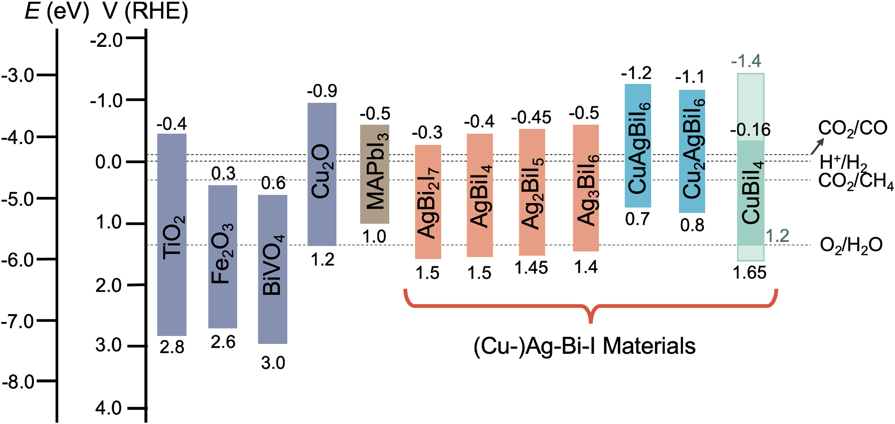
Comparison of the band positions of established semiconductors for photoelectrodes with the band positions of emerging Cu–Ag–Bi–I semiconductors. Band positions are shown relative to the vacuum level, and on the reversible hydrogen electrode (RHE) scale, in which 0 V(RHE) is −4.44 ± 0.02 eV. 143 Band positions were obtained from the literature.35,64–67 Please note that Hu et al. 66 and Zhang et al. 67 reported different sets of band positions and bandgaps for CuBiI4. Pairs of band extrema are given in the same colour (green or black).
Future perspectives for ternary and quaternary compounds from the CuI–AgI–BiI3 phase space
(Cu–)Ag–Bi–I compounds have many exciting emerging applications. To fully explore these areas, it will be important to resolve fundamental questions about these materials and gain further understanding of their process–property–structure–performance relationships in order to more rationally optimise these compounds. In the longer term, it will be important to consider how Cu–Ag–Bi–I materials could be manufactured sustainably and reliably at scale.
Important fundamental questions
One of the key fundamental questions is the nature of charge-carrier transport, and how it is influenced by coupling to phonons in the material. Recent works on Bi-based compounds have shown a wide prevalence of carrier localisation due to charge-carrier coupling to acoustic phonons.1,62,63 Buizza et al. 62 have provided insights into this phenomenon in Cu–Ag–Bi–I compounds, but it will be important to extend this over a wider range of stoichiometries and crystal structures. Such insights will be valuable to guide the community to design (Cu–)Ag–Bi–I compounds that could avoid carrier localisation and exhibit long diffusion lengths.
Another important question is the role of defects in the bulk and surface of (Cu–)Ag–Bi–I materials. Although defect tolerance is predicted in materials with strong s-orbital character from heavy-metal pnictogens, 13 the VB DOS in the case of Ag–Bi–I and Cu–Bi–I compounds is dominated by d-orbitals from the transition metal A-site cation. The picture is further complicated by the cation disorder present in compounds containing Ag and Bi, which have the same ionic radii. Joint experimental–computational investigations would be valuable and may guide the community towards compositions that could exhibit defect tolerance, or provide guidance on how materials can be processed to avoid the worst traps. In particular, it is important to understand how ion migration can be suppressed in these materials (e.g. in LHPs, fullerene ETLs suppress ionic conduction 95 ). Doing so reduces the extent to which ionic conduction obscures the effects of trap states on the capacitance versus frequency spectrum, thus allowing more accurate determination of the traps present through capacitance-based techniques.
At the inter-grain level, it will be important to understand how defects at grain boundaries affect non-radiative recombination and charge-carrier transport. Such characterisation may be accomplished by cathodoluminescence measurements,146,147 but in the case of Cu–Ag–Bi–I materials is complicated by the weak luminescence present in these materials. EBIC measurements can also be used to link grain structure to charge-carrier properties and early attempts from Pai et al. 65 highlight that grain boundaries and interfaces act as active channels for charge-carrier extraction. Another important intergranular property is microstrain, which is influenced by the degree of misorientation between grains and extended defects (e.g. dislocations). The degree of misorientation can be measured by electron backscatter diffraction (EBSD), or geometric phase analysis from transmission electron microscopy images. Recent EBSD measurements with LHPs have shown that greater misorientation results in increased non-radiative recombination.148,149 Similar investigations with Cu–Ag–Bi–I can reveal the true size of grains (as opposed to assuming that the microstructure found in SEM images are grains), and guide the optimisation of film processing to improve optoelectronic properties.
Finally, it will be important to understand the degree of ion migration in Cu–Ag–Bi–I, and how ions are segregated macroscopically over the entire film. Hysteresis has been widely found in Cu–Ag–Bi–I solar cells, and ion migration is believed to be the cause of device degradation in some cases. Indeed, Ye et al. 31 have proposed that iodide vacancy migration is responsible for resistive switching in micron-thick AgBiI4 films.
Process–property–structure–performance relationships
Currently, it is common to report the stoichiometry of Cu–Ag–Bi–I materials based on the starting stoichiometry used in solution synthesis. However, the diffraction patterns of many related stoichiometries are very similar, making phase determination challenging. This is complicated by the presence of phase impurities, such as AgI-based phases, 105 or other Cu–Ag–Bi–I stoichiometries. Furthermore, investigations into new materials as thin films result in peaks being absent due to texturing, which further complicates accurate phase identification. In-depth studies into powder samples or single crystals to better understand the crystal structure would be important, as would the use of techniques to measure the bulk composition of compounds (e.g. mass spectrometry, Rutherford backscattering spectrometry, or X-ray microanalysis).
Beyond the processing of the absorber itself, it will be important to understand how the processing of charge-selective layers on top of the Cu–Ag–Bi–I influence its properties. For example, we and others have found that the addition of tert-butylpyridine into spiro-OMeTAD causes the partial dissolution of the Cu–Ag–Bi–I film. In addition, it will be important to understand more about how the charge-transport overlayer influences the stability of the Cu–Ag–Bi–I. For example, we have found that Ag–Bi–I thin films, made by hot casting, degrade in ambient air, whereas many groups have reported that full devices are stable in ambient air for several days to months (see the ‘Device stability’ section). The higher apparent stability in devices rather than bare thin films may be due to the role of the overlayer in preventing the ingress of moisture from the air, as well as a more optimal morphology being less susceptible to moisture-induced degradation. For example, Hsiao et al. 105 found that films with larger grains led to solar cells that degraded more slowly under operation. Thus far, groups have reported Cu–Ag–Bi–I stability mostly based on XRD measurements of the bulk film and the performance of the final photovoltaic devices.22,40 But it will be important to understand whether changes in the film properties occur when exposed to ambient air without a protective HTL that are not detected by XRD, such as the formation of amorphous regions due to moisture ingress, or due to changes in morphology after ageing in air. Furthermore, it is important to establish more precisely the range of conditions (namely vacuum level and beam flux density) for characterising Cu–Ag–Bi–I thin films without causing changes in the sample during measurement.
Sustainable processing at scale
Finally, although current efforts have overwhelmingly focused on a simple solution processing for preparing and investigating Cu–Ag–Bi–I thin films, devising more scalable and reproducible methods of synthesising these materials will be required for future commercial applications. Recently, Hsiao et al. 105 demonstrated the deposition of Ag3BiI6 by thermally-assisted doctor blading, achieving solar cells with 2.03% PCE in devices with 1 cm2 area, comparable with the performance of small 4 mm2 devices (2.77% PCE). Further efforts to increase the performance of large-area devices, as well as increasing the active area towards 10 cm2 and beyond are needed. Achieving this through solution processing is complicated by the difficulty in achieving dense morphology in these Cu–Ag–Bi–I films, which may be due to how the precursor molecules coordinate with the solvent. 46 Furthermore, it will be important to consider the speed of processing films, since this has a direct influence over the cost of manufacturing. 113 It is also important to devise large-scale manufacturing routes for devices that have low thermal budget (and therefore low CO2eq footprint), with low synthetic complexity, and do not make use of toxic solvents and precursors. 24
Conclusions
In conclusion, over the past few years, ternary and quaternary compounds from the CuI–AgI–BiI3 phase space have transformed from relative obscurity to intriguing materials for optoelectronic applications. Beginning with initial reports in photovoltaics in 2016, these materials have now been explored for energy harvesting, photodetection, radiation detection, memristors, and artificial synapses for neuromorphic computing. The potential application space can be much broader, with opportunities also in photocatalysis and solar water splitting. This rich diversity in possible applications stems from the strong absorption of light, stable bandgaps in the range of 1.6 to 1.9 eV, as well as the high degree of tunability in a range of structural and optoelectronic properties by controlling the composition. At the same time, the fundamental understanding of these materials is at a nascent stage, and more in-depth insights into the nature of charge carriers and charge carrier transport are needed, as well as a deeper understanding of the role of defects, ion migration and grain boundaries. Furthermore, the rich chemical diversity in the Cu–Ag–Bi–I family of materials should be exploited more, exploring compounds beyond Ag–Bi–I and Cu–Bi–I. Such explorations should be guided by new insights into these materials, such as the role of structure on carrier localisation. On the more applied end of the scale, future efforts should also focus on developing the growth of these materials by scalable, rapid and sustainable methods to position these materials for possible commercial applications.
Footnotes
Acknowledgements
The authors would like to acknowledge the input and helpful discussions with Christina (Chuijiang) Kong (孔垂江) and are saddened by her passing prior to the completion of this review.
Declaration of conflicting interests
The authors declared no potential conflicts of interest with respect to the research, authorship, and/or publication of this article.
Funding
The authors disclosed receipt of the following financial support for the research, authorship, and/or publication of this article: Huimin Zhu and Fabien C.P. Massabuau received funding from Iberdrola through the ‘Energy for Future (E4F) Postdoctoral Fellowship’ (Marie Skłodowska-Curie Grant Agreement no. 101034297). Ivan Turkevych received support from the Japan Society for the Promotion of Science, JSPS KAKENHI (grant no. 21K05250). Robert L. Z. Hoye, Hugh Lohan and Pengjun Liu received support from a UK Research and Innovation (UKRI) Frontier Grant (grant no. EP/X022900/1), awarded via the European Research Council Starting Grant 2021 scheme. Hugh Lohan also thanks the Department of Chemistry at the University of Oxford for Support. Robert L.Z. Hoye, Huimin Zhu, Hugh Lohan and Pengjun Liu received funding from the Henry Royce Institute Industrial Collaborative Programme scheme, funded by EPSRC (grant no. EP/X527257/1). Fabien C.P. Massabuau received funding from the Engineering and Physical Sciences Research Council (EPSRC; grant no. EP/V034995/1), and the Royal Society (grant no. RGS/R1/201236). Robert W. Martin recevied support from EPSRC: University of Strathclyde – Equipment Account ‘Nanoanalysis for Advanced Materials and Healthcare’, grant nos. EP/K011952/1 and EP/N010914/1. Robert L. Z. Hoye received funding from the Royal Academy of Engineering through the Research Fellowship scheme (grant no. RF/201718/17101), as well as EPSRC (grant no. EP/V014498/2).