
Abstract
The growing amount of electronic waste is a global challenge: on one hand, it poses a threat to the environment as it may contain toxic or hazardous substances, on the other hand it is a valuable ‘urban mine’ containing metals like gold and copper. Thus, recycling of electronic waste is not only a measure to reduce environmental pollution but also economically reasonable as prices for raw materials are rising. Within electronic waste, printed circuit boards (PCBs) occupy a prominent position, as they contain most of the valuable material. One important step in the overall recycling process is the evaluation and the value estimation for further treatment of the waste PCBs (WPCBs). In this article, we introduce a method for value estimation of entire WPCBs based on component detection. The value of the WPCB is then predicted by the value of the detected components. This approach allows a flexible application to different situations. In the first step, we created a dataset and labelled the components of 104 WPCBs using different component classes. The component detection is performed on dual energy X-ray images by the deep neural object detection network ‘YOLO v5’. The dataset is split into a training, validation and test subset and standard performance measures as precision, recall and F1-score of the component detection are evaluated. Representative samples from all component classes were selected and analysed for the valuable materials to provide the ground truth of the value estimation in the subsequent step.
Introduction
Over the past years, the amount of electronic waste has been rapidly growing, and an end of this trend is not in sight. According to the Global E-waste monitor 2020, 53.6 million metric tonnes (Mt) of e-waste were generated worldwide in 2019, of which only 17.8% were officially documented as properly collected and recycled. It increased by 9.2 Mt since 2014 and is projected to grow to 74.7 Mt in 2030 (Forti et al., 2020).
The current development of printed circuit boards (PCBs) has followed a linear economy value chain, resulting in significant waste generation and loss of value at the end-of-life stage. To address this issue, the electronics industry needs to transition towards more sustainable practices. Chakraborty et al. (2022) provided an overview of potential solutions and opportunities that can arise from the increased utilization of emerging sustainable materials and resource-efficient manufacturing techniques. Today, the industry faces significant challenges in adopting green consumerism, including sustainable sourcing, production, product design, customer awareness and regulatory compliance (Karagiannopoulos et al., 2023). Approaches like reverse logistics (RL) and closed-loop supply chain (CLSC) of Waste Electrical and Electronic Equipment have gained acceptance and widespread practice in manufacturing industries over the last 20 years due to growing environmental regulations, the potential recovery of valuable material resources, and the need for sustainable business practices (Islam and Huda, 2018). Electronic waste presents unique challenges within RL and CLSC due to its rapid growth, driven by short product life cycles and changing consumer attitudes towards disposal. Despite the significant volume of e-waste generated, current literature does not adequately distinguish the RL and CLSC processes for e-waste from general waste streams. In 2019, the value of raw material in the global e-waste is approx. $57 billion USD. Thus, for both ecological and economic reasons, it is beneficial to recycle as much material as possible from e-waste, which needs automation to handle the mere amount. In fact, almost all electronic equipment contains PCBs and a huge part of the valuable raw materials is contained on them, for example, in integrated circuits (ICs), ball and pin grid arrays (BGA/PGAs) connectors and capacitors. In addition, the concentration of valuable metals as gold, platinum group metals, silver, tantalum, etc. in waste printed circuit boards (WPCBs) is considerably higher than in primary raw materials and has a smaller carbon footprint than producing these materials from mining (Hagelüken and Goldmann, 2022). This work focuses on the challenges that are related to the recycling of WPCBs. To ensure optimal efficiency in recycling and maximum recovery of the valuable materials mentioned above, it is desirable to estimate the content and value of WPCBs. After collection of the e-waste and extraction of the WPCBs, the value of large batches of WPCBs currently needs to be estimated by human experts on basis of random samples, a task that is time consuming, costly and error prone. This situation can impede the price discovery between seller and buyer. For an automated evaluation and value prediction, however, a reliable sensor system would be beneficial for both sides. First publications on automatic component detection for automatic classification and the estimation of the raw material value of entire WPCBs are limited to reflective imaging techniques as visible RGB (Silva et al., 2021, Sudharshan et al., 2020), NIR or hyperspectral imaging (Sudharshan et al., 2020). However, these imaging technologies are limited to the surface of the WPCB and require the components to be visible on the surface. For single-sided WPCBs, they require a correct orientation of the components towards the camera and for double-sided WPCBs, they are limited to the components on only one side. X-ray imaging provides the advantage of being a transmission technique, that is, it allows to ‘look through’ the object and thus, for both single- and double-sided WPCBs, it is irrelevant which side is facing the camera. Furthermore, X-ray imaging is less sensitive to dust and dirt on the WPCBs, as it is found in typical recycling environments.
The proposed method does not explicitly identify individual component types and manufacturers and does not explicitly determine which valuable material is contained within every single component as this would require a huge data base of millions of components that would likely look very similar. Rather, we estimate the composition of valuable materials from mean values of a limited number of different component classes, like ICs, BGAs/PGAs, tantalum capacitors, connectors, etc.
Materials and methods
Our approach for value estimation of WPCBs is based on X-ray images which are measured with an X-ray system and consists of two subsequent processing stages. The first stage is a deep neural object detection network that is used for localization and recognition of component types (which are hereinafter referred to as component classes). The second stage is a mathematical model for the estimation of the value of the underlying WPCB based on the detected components of the first stage and a chemical value analysis of a few components. The chemical value analysis is basis for the assignment of the component classes to its material value.
The experimental setup of this article has two main emphases:
Which object detection quality can be reached via deep neural networks in terms of: 1.1. Different deep neural object detection network designs 1.2. The number of component classes to be detected (more components enable a more curate value assignment in the second stage) 1.3. The equipped components on the WPCB side (single-sided versus double-sided)
Can a more accurate value estimation of WPCBs be realized by increasing the number of classes and also an enlargement of the number of components per classes regarding their value compared to our publications with four component classes (Firsching et al., 2022; Pomberger et al., 2022)
Measurements
The X-ray transmission (XRT) images were performed using a Comet MXR-225HP/11 X-ray source operating at 100 kV and 15 mA and a Hamamatsu C10800-09FCM-C dual energy line detector with a pixel pitch of 0.4 mm. The measurements were carried out in our lab with the WPCBs on a conveyor belt moving with a speed of 0.45 m s. Standard linear image correction methods as offset/gain correction were applied. The X-ray energy channels were normalized to the bright value leading to image values in the range [0, 1]. Subsequently, the natural logarithm was applied.
Computational environment
The hardware setup for the machine learning part consisted of a cluster of four workstation computers with single CPU (AMD Ryzen 72700 with eight cores), 64 GB of RAM and a single GPU each. Three computers were equipped with GTX 1080 Ti and one with RTX 3060 GPU, which enables the use of CUDA (Kirk, 2007; Ilievski et al., 2018). To train and use the model, PyTorch 1.7.1 and CUDA 11.0 were used.
Database
The database consists of 104 WPCB samples, of these samples 77 are covered on one side with components (single-sided) and 27 samples have components on both sides (double-sided). An illustration of XRT images of WPCBs are shown in Figure 1, which are acquired with the above described measurement technique.
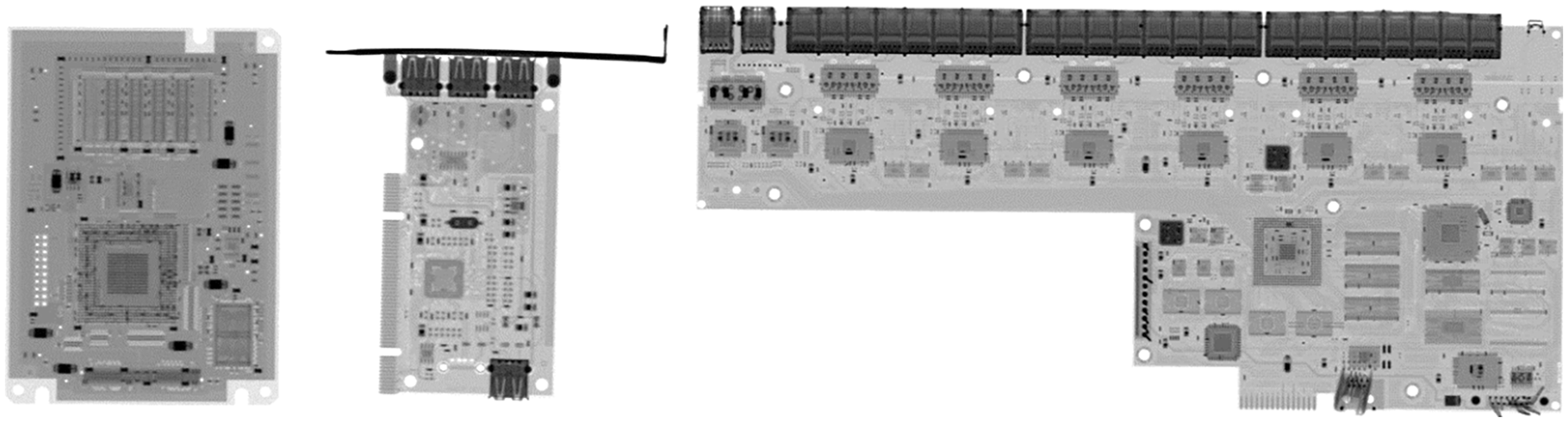
Illustration of three WPCB X-ray transmission images ID005 (left), ID025 (middle) and ID099 (right).
WPCB components were grouped according to their design to enable the machine learning model to learn related features of the components. In addition, this is intended to provide a rough reference to their material composition and an accumulation of certain materials in this group, which results in clusters of higher- and lower-graded components.
The database is fully annotated with seven different component classes: IC, tantalum capacitor (TC), ball and pin grid arrays (BGA/PGA), quartz crystal oscillators (Q), connectors that are subdivided into low-grade (Clg), high-grade (Chg) and Goldfingers (G). In total, the database consists of 5471 components.
Here, annotation refers to the determination of the ground truth that is required for a supervised deep learning object detection task. The annotation includes bounding box coordinates to specify the location of WPCB components, and component class labels to indicate the type of each component within the bounding box. Figure 2 illustrates an example on an annotated WPCB in form of a pseudo-colour representation which is the input in the object detection model.
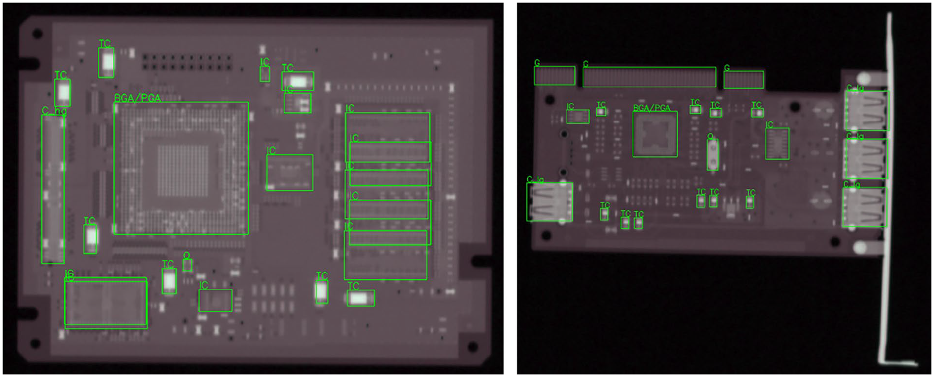
Two examples of annotated WPCBs, ID005 (left) and ID025 (right), are displayed in a pseudo-colour scheme which corresponds to the model input. Further the ground truth bounding boxes (positions) and names of the component classes are shown in green.
The datasets for the experimental setup are prepared as follows. The data and corresponding labels are split into three sets (training, validation and test) with the target that each set includes the same percentage of single-sided and double-sided WPCBs as well as a similar percentage of all classes. This is a common machine learning procedure to ensure that the model performance can be evaluated consistently during the training phase – with the validation set – and for a final independent evaluation with the data from the test set. The total amount of samples and component classes are listed in Table 1.
Quantity of the underlying single-sided (SS) and double-sided (DS) WPCBs and their numbers of component classes within each set.
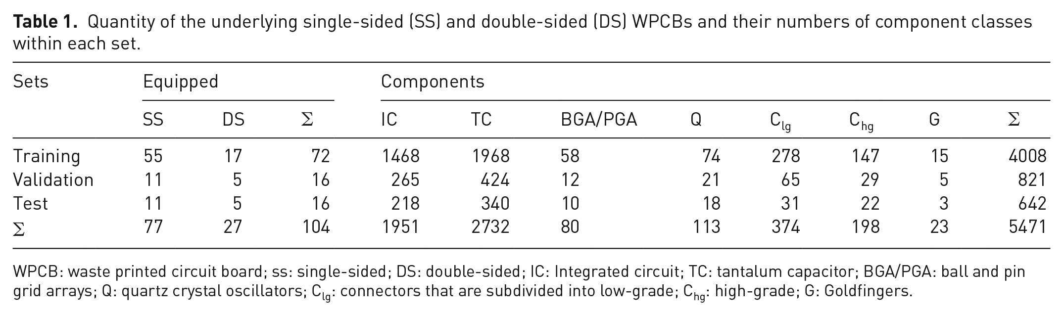
WPCB: waste printed circuit board; ss: single-sided; DS: double-sided; IC: Integrated circuit; TC: tantalum capacitor; BGA/PGA: ball and pin grid arrays; Q: quartz crystal oscillators; Clg: connectors that are subdivided into low-grade; Chg: high-grade; G: Goldfingers.
Models
The deep neural object detection network, which was used to solve the detection task, is based on the YOLOv5 architecture. The YOLO (You Only Look Once) is an object detector, which was designed with the goal to be able to detect as many different object classes as possible in a short time with good accuracy in an image. In order to detect all learned classes, the YOLO, unlike classical convolutional neural network (CNN), requires only one network pass. Since the YOLO looks at an image only exactly once, it belongs to the so-called single shot detectors. The used YOLOv5 (Jocher et al., 2021) builds significantly on its predecessor YOLOv3 (Redmon and Farhadi, 2018). A core element of the YOLO are the anchor boxes, which were introduced with the YOLOv2 (Redmon and Farhadi, 2017).
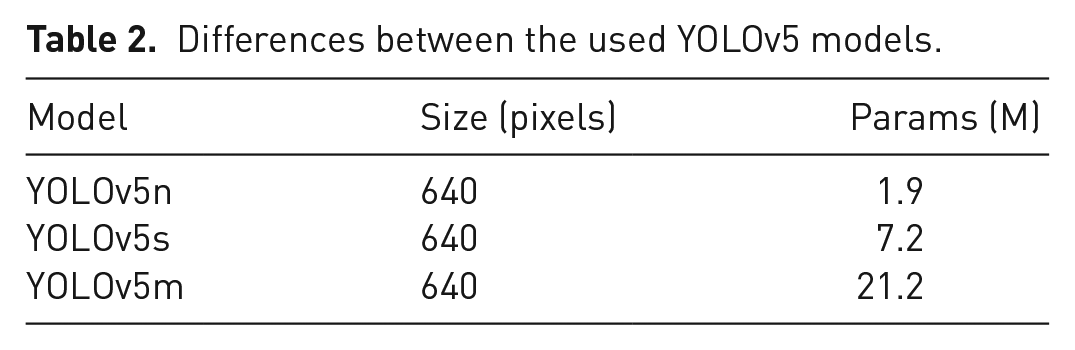
Several pre-trained configurations of this model based on the MS COCO dataset (Lin et al., 2014) were used. As shown in Table 2, three different models, that is, the nano (n), small (s) and medium (m) model, have been designed and trained and were evaluated. These models differ in depth (number of layers) and width (layer-size), which can have a high impact on the number of parameters in the neural network but have the same input image size.
Differences between the used YOLOv5 models.
Each model-setup is based on the architecture given in Figure 3. This architecture can be split into Backbone, Neck and Output. The backbone is a CNN, which creates different granularities and image features at the same time. The Neck is a set of network layers that combine image features of different granularities and transmit these to the Output. The Output contains prediction layers for the three different scales, which generates the coordinates of the bounding boxes of the recognition targets and predicts the class of the targets object.
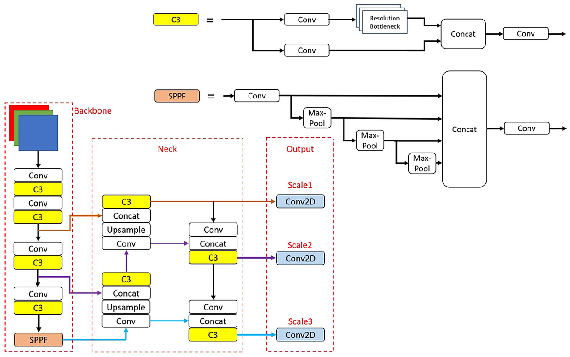
Architecture with its specific connections and the coarse separation into Backbone, Neck and Output. C3- and SPPF-Modules are shown in detail.
At the beginning, the input data in the backbone is scaled to 3 × 640 × 640. According to X-ray data the first channel includes the high energy values, the second channel includes the low energy values, and the third channel contains the mean over both energies. Then it goes through a series of convolution layers (Conv). The C3 modules contain two convolution layers connected in parallel, whereby a resolution bottleneck (Li and Liu, 2019) is attached to one of them. With a concatenation (Concat), both strings are connected and further processed by another Conv module. At the bottom of the backbone is the Spatial Pyramid Pooling Fast (SPPF) module, which is characterized by a pyramidal structure of max-pool layers (He et al., 2014). The neck as well as the output correspond to the structure of a feature pyramid network with a bottom-up path augmentation (Liu et al., 2018). This structure allows the exchange of features across the different levels of granularity both from the bottom up and from the top down.
Each model is trained for 500 epochs. A batch size of eight and input image dimension of 640 × 640 pixels in which the corresponding WPCB samples are centred and rescaled are used. Data augmentation strategies are randomly applied for each iteration step. This includes standard methods like scaling, translate and flipping as well as the Mosaic augmentation, which split the image into four pieces (Bochkovskiy et al., 2020). Additionally, each mosaic piece can be augmented by the standard methods.
Value estimation
The deep neural object detection network described above detects the components mentioned and classifies them. For each WPCB, a list of components with type and position is generated, from which also the size can be determined. From the analysis of the element contents, the average content of relevant elements per component class is known. By applying the value determination model, the specific value of a WPCB for recycling can now be determined based on the detected components. The value determination model can be parameterized and thus adapted to the needs of the respective user. These parameters can, for example, be linked to values such as current raw material prices or the yield of subsequent process steps. This approach allows the value determination model to be adapted very flexibly to the requirements in different application environments, for example the size of the detected objects could be taken into account.
One possible implementation of the value estimation model is to assign a mean value to the components of a class and to sum over all of them to predict the monetary value of the entire WPCB. For this purpose, the sample set was analysed by ICP-OES and the mean gold content of the components of the IC, BGA/PGA and connector (C) classes was determined. Per piece, the results were 0.457 mg for ICs and 4.71 mg for BGAs/PGAs. For the connectors, we have two cases, just one general connector class (C) with 0.914 mg of gold per piece and the sub-class ‘high-grade connectors’ (Chg) with 2.35 mg. At a current gold value (April 2023) of approximately €1820 per troy ounce (31.1 g), or 5.85 ct per mg, this gives a mean value of 2.7 ct per IC, 27.6 ct per BGA/PGA, 5.3 ct per (C) and 13.7 ct per (Chg). The mean mass of the TCs was 767 mg, which at a market price of about €25 per kg in 2022 for tantalum capacitors results in a mean price of 1.9 ct per TC. The values for quartz oscillators and Goldfingers are not yet available.
Results and discussion
In the following, the results of the different experiments are shown. Three designs of the architecture are trained and optimized based on identical dataset splits. For evaluation, we run our experiments ten times and average the results to keep the statistical error low. We use the widely used F-score as described in Goutte and Gaussier (2005) to present the achieved model performance.
The F-score F1 combines recall with precision to provide a clear quality measure where recall is considered to be as important as precision (β = 1). The F1 score ranges from 0 to 1 where F1 = 1 indicates perfect precision and perfect recall.
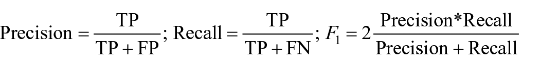
A decision is counted as true positive (TP) if the prediction corresponds correctly to the actual object class and its localization. Correct is denoted here that the intersection over union of the actual object location area and the predicted area of the object class is larger than 50%. Additionally, only objects are counted as correct if the model prediction certainty is larger than 50%. If the model detects the actual object class incorrectly or detects an object at a location where no object actually exists, this is considered as false positive (FP). An object that belongs to a certain class but was not detected by the model is called a false negative (FN).
Next, our test results of the experimental setups are presented:
First, our findings for four different classes of components (IC, TC, C and BGA/PGA) were evaluated for this dataset. This is already published at (Firsching et al., 2022; Pomberger et al., 2022). Therefore, the deep neural object detection network architecture YOLOv5s is used and optimized. The test results (shown in Table 3) reach a F1 score for ICs of 82%, TCs of 74%, Cs of 64% and BGAs/PGAs of 87%. Further the results indicate that the model detects components on single-sided (SS) and double-sided (DS) WPCBs in almost the same precision and quantity based on the underlying X-ray images.
Test results of the model optimized with four classes. The applied architecture is YOLOv5s.
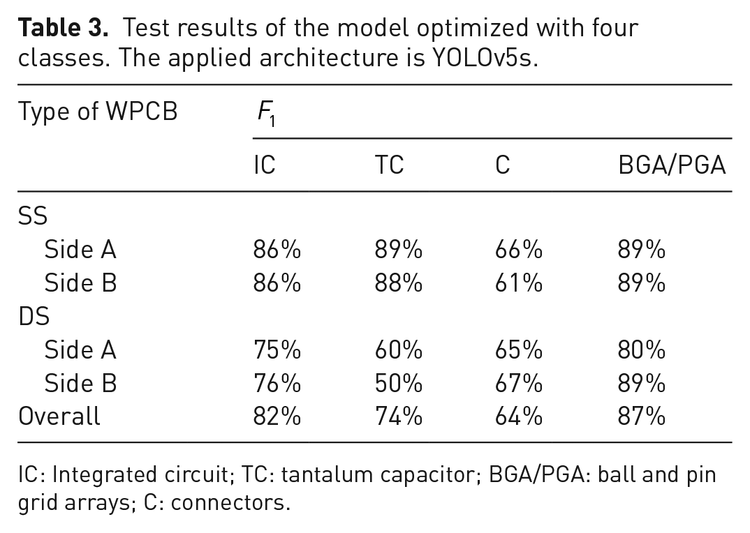
IC: Integrated circuit; TC: tantalum capacitor; BGA/PGA: ball and pin grid arrays; C: connectors.
The overall test results of the YOLOv5s model which was optimized for four different component classes and the value estimation are shown in Table 4.
Test results of the value estimation based on the object detection results.
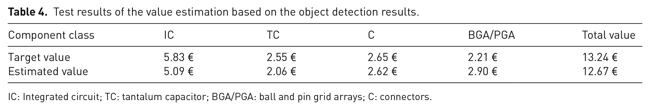
IC: Integrated circuit; TC: tantalum capacitor; BGA/PGA: ball and pin grid arrays; C: connectors.
The test results of the different models with the dataset with additional classes (Q, G, Clg and Chg) are given in Tables 5 to 7. Direct comparison between these models with the models in Table 3 reveals a decrease of the F1 score in all classes. Regarding the TC and IC classes, this is especially due to the large number of small components added to the dataset. These small components from the TC and IC class are difficult to distinguish.
Overall test results of the nano (N) model and additionally the detailed results with double sided WPCBs and single-sided WPCBs only.
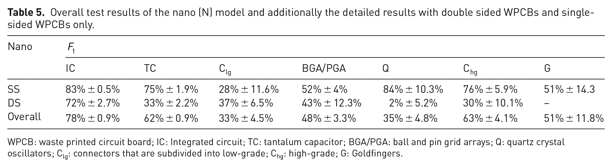
WPCB: waste printed circuit board; IC: Integrated circuit; TC: tantalum capacitor; BGA/PGA: ball and pin grid arrays; Q: quartz crystal oscillators; Clg: connectors that are subdivided into low-grade; Chg: high-grade; G: Goldfingers.
Overall test results of the small (S) model and additionally the detailed results with double-sided WPCBs and single-sided WPCBs only.
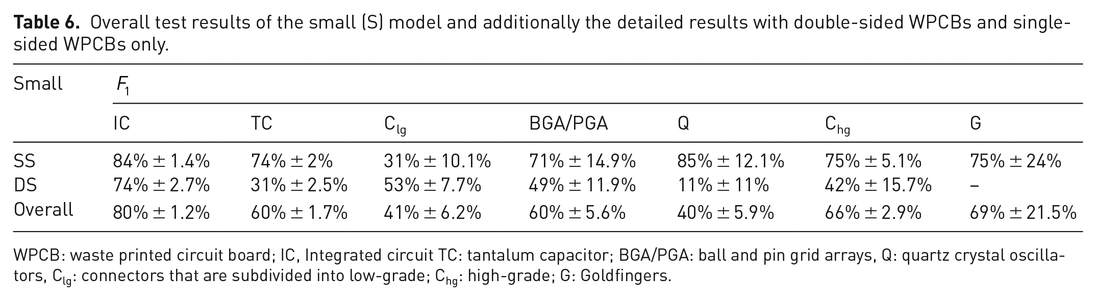
WPCB: waste printed circuit board; IC, Integrated circuit TC: tantalum capacitor; BGA/PGA: ball and pin grid arrays, Q: quartz crystal oscillators, Clg: connectors that are subdivided into low-grade; Chg: high-grade; G: Goldfingers.
Overall test results of the medium (M) model and additionally the detailed results with double-sided WPCBs and single-sided WPCBs only.
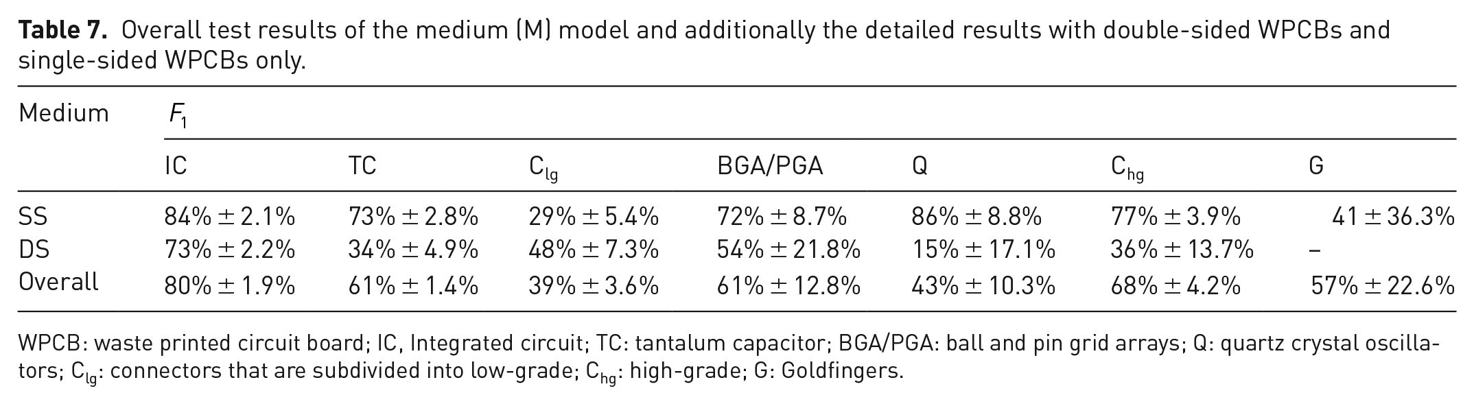
WPCB: waste printed circuit board; IC, Integrated circuit; TC: tantalum capacitor; BGA/PGA: ball and pin grid arrays; Q: quartz crystal oscillators; Clg: connectors that are subdivided into low-grade; Chg: high-grade; G: Goldfingers.
The overall results show that the S and M models score better than the N model. The S and M models are, apart from the low-grade connectors and the Goldfinger class, relatively similar. Due to the possibility of overlapping, components on double-sided WPCBs are harder to detect than on single-sided WPCBs. The classes TC and IC, which are the most represented, achieve the best F1 scores. The low-grade connectors (Clg) achieve better scores on the double-sided WPCBs. This is due to the fact that the Clg on the double-sided WPCBs are mainly placed at the edge, whereas the Clg on the single-sided WPCBs can be more distributed over the board. Furthermore, Figure 4 shows an example of overlapping components on double-sided WPCBs.
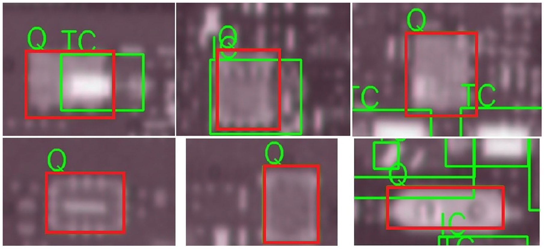
Example of the differences between the samples of the class for quartz crystal oscillators (Q). Ground truth bounding boxes of various classes are shown in the image sections, with the boxes of class Q highlighted in red in each case. While the quartz crystal oscillators often overlap with components of other classes, the components Q also differs in their appearance. For example, the first two components Q in the second-line look quite different in direct comparison. Because of these reasons, these components are more difficult to detect in the used dataset. The image quality is limited by the pixel size of the X-ray detector. It was chosen to allow real-time processing of the image data even at high conveyor belt speed.
Table 8 shows the value estimation for the congruent classes to Table 4. Value estimations for the classes Clg, Q and G are not available yet.
Test results of the value estimation. Processed were the prediction results of the YOLOv5s.
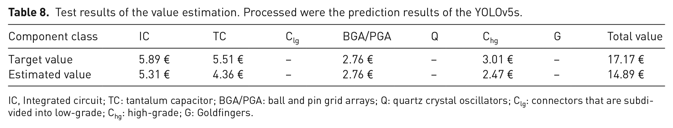
IC, Integrated circuit; TC: tantalum capacitor; BGA/PGA: ball and pin grid arrays; Q: quartz crystal oscillators; Clg: connectors that are subdivided into low-grade; Chg: high-grade; G: Goldfingers.
Summary and conclusion
In this article, we introduced a method for estimating the material value of WPCBs for recycling. The evaluation is carried out on complete, unshredded WPCBs that have been removed from the waste electrical devices. The value of WPCBs varies greatly and depends on the number of components integrated and the mass content of the valuable metals used in the components. It is uncertain if a real value evaluation for single components on the WPCB can be made, as there are millions of different designs of a single component. Furthermore, the quantities of valuable metals in the WPCBs are too small to allow direct sensory measurement for sensor-based sorting. Therefore, the method presented is based on counting the components and determining an average value per component in order to estimate the value of the WPCB. The method is based on the detection of valuable components on entire WPCBs from X-ray images using a machine learning-based object detection network called YOLOv5. We figured out that the YOLOv5 architecture is not only well suited for natural (visible light) images but also for X-ray images. With appropriate data pre-processing of the X-ray images, also models pre-trained with natural images can be used and yield good results using the YOLOv5 model.
We used WPCBs that are populated on one or on both sides. Compared to reflective methods like visible RGB imaging, NIR, SWIR or hyperspectral imaging, XRT imaging has the advantage of being independent on which side of the WPCB is on top. Thus, the reflective methods are challenged by the components that face away from the camera, whereas XRT is not limited in this way. However, with WPCBs populated on both sides with components, the components overlap in the XRT images, which also decreases the detection performance. When comparing the YOLOv5 models that differ in number of layers and layer size (called nano, small and medium), we found the expected trend that larger models perform better in most cases. However, the results are noisy in this aspect and differences are small, especially between ‘small’ and ‘medium’.
Using the deep learning object detection network, different classes could be detected successfully even with a relatively small training set. Different component classes were compared to each other. On one side, only four different classes were used: Ball/pin grid arrays (BGA/PGA), ICs, TCs and connectors (C). On the other side, seven classes were defined. The previous four were extended by Goldfingers (G) and quartz oscillators (Q) and the connector class was divided into two new classes connectors low-grade (Clg) and connectors high-grade (Chg). As to be expected, with more classes and the same, limited number of samples for training, the results deteriorated.
The feasibility of the method for value determination of WPCBs was demonstrated exemplarily for a limited number of WPCBs of high-value WPCBs coming from PC’s, servers and mobile phones. A generalized method for determining the value of all WPCBs, especially for medium- and low-grade WPCBs, is not yet proven. In addition, WPCBs are crushed for easier transport and sorting, so the WPCBs are more likely to be in the form of WPCB flakes. However, the deep neural object detection network shown is currently only trained on whole WPCBs. In the future, the two points mentioned above, firstly the extension to WPCB classes 2–4 (low-grade) and secondly the extension of the training data to WPCB flakes are to be realized; thus, a general method for determining the value and sorting of WPCBs will be established.
The economic and ecological benefits of this method have not yet been fully investigated. It is still to be evaluated whether the separation and concentration of different materials (gold, tantalum, palladium, etc.) has an economic advantage, which would be to obtain higher market prices for the concentrated material. The ecological advantage of the method would be to use less energy in the recovery of the valuable materials from the WPCBs and thus save CO2. An additional ecological benefit would be to reduce the consumption of chemical substances in the recovery process of the metals by a high pre-concentration of the valuable materials. As only those WPCBs will be processed further that have an adequate concentration of the wanted materials, the entire mass stream that needs to be processed can be reduced while keeping the recovery rate at a high level.
Footnotes
Declaration of conflicting interests
The authors declared no potential conflicts of interest with respect to the research, authorship, and/or publication of this article.
Funding
The authors received no financial support for the research, authorship, and/or publication of this article.