
Abstract
The evolution of microstructure strain partitioning during quasi in situ tensile loading of grade 2205 duplex stainless steel has been investigated. Digital image correlation revealed the development of tensile strain initially in austenite and at interphase boundaries, and further extending into the ferrite with increasing load. Higher resolution digital image correlation observations indicated strain hardening of austenite, followed by deformation of the ferrite. Digital image correlation analysis of a 20% cold-rolled microstructure revealed tensile strain development at interphases, with discrete tensile and compressive strain pockets observed within the austenite. X-ray diffraction measurements indicated the presence of tensile stresses primarily developing in the ferrite, with full-width at half maximum values indicating plastic strain accumulation primarily in the austenite. The effect of tensile loading on Volta potential differences, obtained via scanning Kelvin probe force microscopy, highlighted the development of discrete anodic and cathodic sites with the introduction of strain. A Volta potential roughness parameter (ΨRa) is introduced describing Volta potential changes as a function of strain. This observation supports the concept of an enhanced propensity of local electrochemical activity with increasing applied strain in duplex stainless steel.
Keywords
Introduction
Duplex stainless steels are nowadays used for application in demanding environments due to their excellent mechanical and electrochemical properties. 1 A balanced ratio of ferrite (δ) and austenite (γ) is typically present in duplex microstructures, 2 with the grain morphology elongated in rolling direction, leading to banded structures of discrete austenite grains embedded in a ferritic matrix. 3 The body-centred-cubic (bcc) ferrite has different mechanical properties compared to the face-centred-cubic (fcc) austenite, 4 and consequently, there is a mismatch during deformation in the microstructure, leading to strain and stress partitioning. 5 Residual strain is typically present in duplex microstructures due to different thermal expansion coefficients of both phases, resulting in the formation of heterogeneous strain fields in the microstructure.6,7
Grade 2205 duplex stainless steel is currently proposed as material option for intermediate-level radioactive waste (ILW) storage containers in the United Kingdom.8,9 It is therefore important to assess its microstructure with respect to the development of local strain and stress fields, primarily to understand how stress and strain affect corrosion and crack nucleation propensity. Knowledge about the evolution of critical strain components and their relation to corrosion sites in the microstructure will allow optimisation of material performance.10–12
The aim of the work reported in this article was to obtain information about the effect of strain partitioning and its relation to local changes in Volta potentials in grade 2205 duplex stainless steel. Microstructure observations during quasi in situ tensile loading obtained via digital image correlation (DIC) are compared to stress and strain development measured by X-ray diffraction (XRD) and the development of Volta potential changes in microstructure obtained via scanning Kelvin probe force microscopy (SKPFM). The implications of these observations are discussed in light of microstructure optimisation for application of duplex stainless steel in demanding environments.
Experimental
A solution-annealed (1100 °C, water quench) grade 2205 duplex stainless steel plate with 10-mm thickness and a chemical composition of 22.4% Cr, 5.8% Ni, 3.2% Mo, 1.5% Mn, 0.4% Si, 0.18% N, 0.016% C, 0.021% P, 0.001% S and Fe (bal.) was used in this study. Micro-tensile specimens with 50-mm length, 1-mm thickness, 25-mm gauge length and 3-mm gauge width were machined from as-received and 20% cold-rolled plate material. The surface of all micro-tensile specimens was ground to 4000-grit using SiC sandpapers followed by a 3- and 1-µm polishing finish using diamond paste. Electrolytic etching was performed to reveal the microstructure in 40% KOH at 5 V for 10 s, resulting in stained ferrite.
DIC was performed on a set of images taken during straining of micro-tensile specimens of as-received and 20% cold-rolled samples using a micro-tensile testing machine from Kammrath and Weiss (Dortmund, Germany). Straining was performed in discrete displacement increments of 5–10 µm using an elongation rate of 0.3 µm/s. The force–displacement values were recorded from the crosshead/actuator of the tester. Macroscopic strain was calculated from the applied displacement over the total gauge length, and stress was determined from the applied force as a function of the initial cross-sectional area of the micro-tensile specimen.
The as-received specimen was strained to 0.8% macroscopic strain with images of the microstructure recorded using a Keyence VHX-200 optical microscope at 400× magnification. This corresponded to an imaged region of 800 × 600 µm2. The image resolution was 1600 × 1200 pixels, resulting in a pixel size of 0.5 µm. The average grain size of ferrite and austenite was 7 ± 1 and 6.5 ± 1 µm, respectively, as reported in earlier work. 13 The tensile specimen was further strained to 1.4% macroscopic strain (+0.6% strain) and images of the microstructure obtained using the Keyence VHX-200 optical microscope at 1000× magnification, resulting in an imaged microstructure area of 320 × 240 µm2 and a pixel size of 0.2 µm. The specimen was then unloaded, the whole set-up transferred to an FEI Quanta 650 scanning electron microscope (SEM) and the sample reloaded to 6% total macroscopic strain, with images recorded in secondary electron (SE) mode at 500× magnification. This corresponded to a horizontal field of view of 600 µm, and the image resolution in the SEM was 2048 × 1768 pixels, giving a pixel size of 0.3 µm. The 20% cold-rolled specimen was strained to 4% macroscopic strain and the microstructure imaged using a Keyence VHX-200 optical microscope at 200× and 600× magnification. This corresponded to an imaged microstructure area of 1600 × 1200 and 533 × 400 µm2, respectively, resulting in a pixel size of 1 and 0.3 µm, respectively. The image resolution was 1600 × 1200 pixels. Table 1 gives a summary of all straining experiments performed with key parameters.
Overview of strain measurements and pixel resolution for DIC analysis.
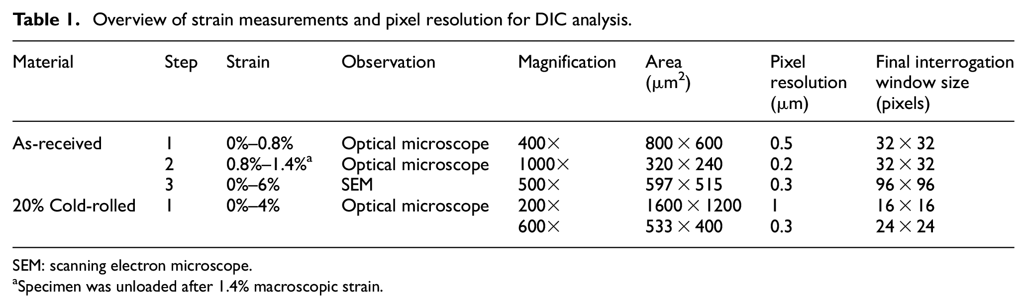
SEM: scanning electron microscope.
Specimen was unloaded after 1.4% macroscopic strain.
DIC of each sample was carried out after introducing a small amount of pre-strain (0.02%–0.04%) to observe the initial microstructure response. Images were then obtained at the end of each applied strain increment, and DIC of optical and SEM images of successive increments was carried out. DIC analysis was also carried out for images acquired at the end of each test and correlated with the first image of the unstrained condition.
LaVision DaVis (V8.2.2) was used for DIC analysis with all images converted into 8-bit greyscale. Shift and rotation correction was applied to correct for rigid body translations, and a 2D deformation time-series using integral correlation with sum of differential vector fields was performed. A geometric mask was applied, and multiple pass iterations (decreasing) with 512 × 512 or 256 × 256 pixels interrogation window size, 25% window overlap, three passing sequence, followed by a smaller window size (between 96 × 96 and 16 × 16 pixels) with 50% window overlap and two passing sequence, were applied for displacement vector calculations. A correlation coefficient of 0.3 was used. The maximum normal strain and maximum shear strain were obtained for each test.
To determine the noise of the system (strain uncertainty), two images of a non-deformed sample were taken and a small amount of in-plane rigid body translation was applied. DIC was applied to these images and the maximum strain uncertainty determined, with this analysis performed for each microstructure and magnification used in this study. The strain uncertainties were obtained for different interrogation window sizes, as summarised in Figure 1. Strain uncertainties were predominantly localised in the austenite due to fewer features formed by KOH etching. Therefore, strain uncertainties in the ferrite were in general at least one order of magnitude smaller than those reported in Figure 1.
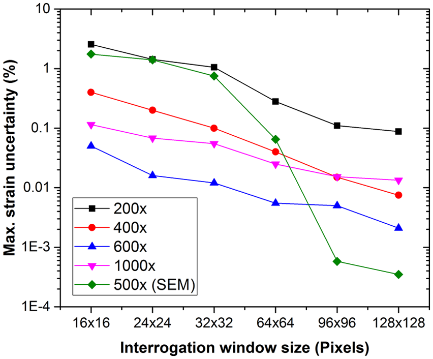
Maximum strain uncertainties of DIC-processed images for each image dataset.
XRD surface residual stress measurements were performed on a flat tensile specimen with a gauge length of 40 mm, a width of 10 mm and thickness of 2 mm. The specimen was at first mechanically ground to 1200-grit using SiC sandpapers, followed by electropolishing using a 20 vol% perchloric acid and 80 vol% methanol electrolyte at 20 V at a temperature of −35 °C, for 60 s. XRD measurements were carried out on a Proto iXRD Combo testing machine (Proto Manufacturing Inc., Taylor, MI, USA), equipped with a two-detector system. Cr and Mn X-ray sources were used to measure the strain in ferrite and austenite, respectively. The tensile sample was loaded to pre-set displacements with the strain measured in one phase, followed by changing the X-ray tube and measurement of strain in the other phase. The strain in the ferrite and austenite was measured under loading condition, after the application of three discrete displacement steps at 0.05%, 0.1% and 0.19% macroscopic strain, followed by a measurement after unloading the sample. The measurement position was in the centre of the gauge section of the specimen.
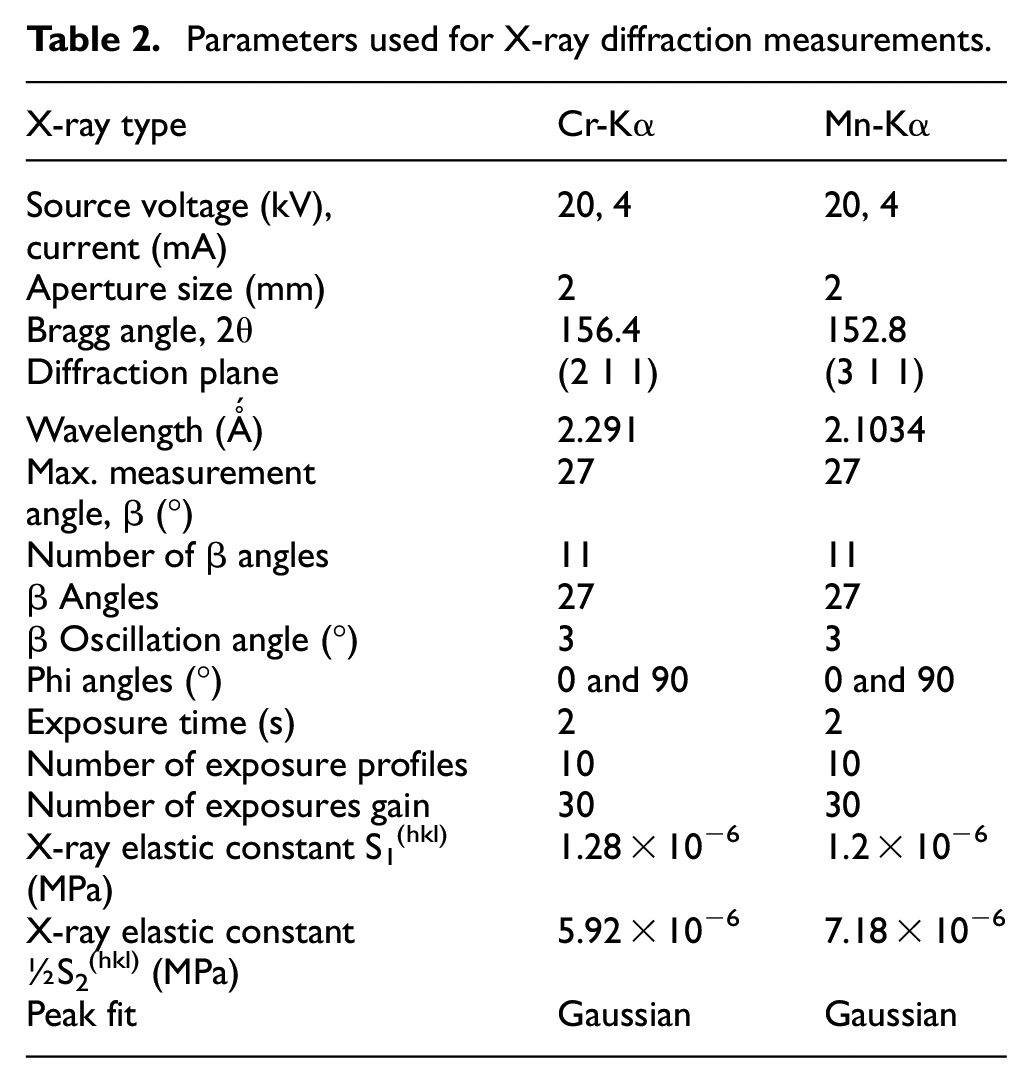
All XRD measurement parameters are listed in Table 2. Figure 2 describes schematically the experimental set-up, with the image insert in Figure 11 showing the tensile rig used and the corresponding sample coordinate system. Prior to the test, the X-ray diffractometer was calibrated using a stress-free standard (powder material provided by the manufacturer) and a stressed standard (ferritic and austenitic steel samples provided by the manufacturer) to accurately determine stress-peak positions. The multiple exposure technique with 11 measurement angles was used for inter-planar d-spacing measurements. Two stress tensors at 0° and 90° phi angles were obtained; with phi 0° being parallel to the loading axis of the sample (each measured orientation corresponds to the stress direction as specified in the image insert in Figure 2). The measurement position was in the centre of the specimen. Stress and full-width at half maximum (FWHM) values of the peak intensities were obtained from the Proto iXRD Combo software for each measurement and plotted versus macroscopic strain.
Parameters used for X-ray diffraction measurements.
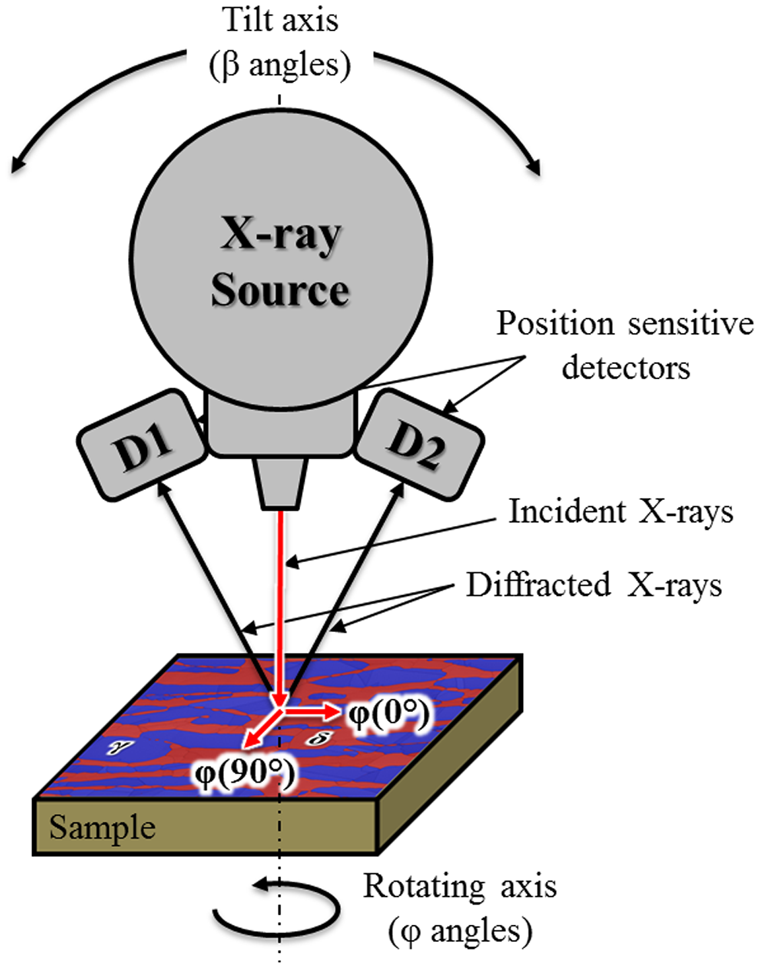
Schematic illustration of X-ray diffraction measurement set-up.
SKPFM measurements were performed using a Dimension 3100 atomic force microscope (AFM) from Digital Instruments (Tonawanda, NY, USA). The theoretical background and a description of SKPFM measured Volta potentials are described elsewhere.12,14–16 In summary, SKPFM is typically operated in a two-pass mode, with the first pass determining the surface topography, followed by a second pass carried out at a pre-determined height (typically 50–100 nm) to measure Volta potential differences. The measured Volta potential difference between the tip used and the surface reflects the electronic activity of the metal surface at this analysis point. OSCM-PT (Pt-coated Si) probes were used for Volta potential (ΔΨ) measurements, with a lift height of 50 nm. The SKPFM scan size was 80 µm × 80 µm. Data analysis was performed with the software NanoScope Analysis version 1.5. Topography and potential maps were flattened using first-order flattening in order to enhance contrast, but quantitative data analysis was performed on raw data without flattening. SKPFM data acquisition was carried out with 512 × 512 pixel resolution, with all values reported relative to the work function of the AFM-tip (Pt-tip). Potentials measured with higher and lower values with respect to the tip indicate net anodic and net cathodic activity, respectively. The Volta potential distribution was expressed as a Volta potential roughness (ΨRa) parameter to describe Volta potential variations as a function of the ferrite and austenite phase. The roughness parameter was determined from Volta potential maps using NanoScope Analysis 1.5 software (Bruker, Santa Barbara, CA, USA), with Ra of the Volta potential line profile in each phase extracted and quantified. Ra describes the arithmetic average of the absolute values of roughness profile ordinates. 17 Here, Ra was determined by extracting the mean of Volta potential variations in each profile measured over each crystallographic phase. One region in the centre of the sample was mapped for Volta potential differences, with 0%, 0.23% and ≈10% total macroscopic strain, with the latter being a different region than the others. The sample was measured in the unloaded condition and was therefore removed from the tensile tester for each SKPFM measurement.
Results and discussion
The as-received microstructure had a ratio of 43 ± 1% ferrite (δ) and 57 ± 1% austenite (γ) determined via image analysis of optical micrographs. The austenite was discrete with an island-like morphology, surrounded by the ferrite matrix. Typical microstructures of the as-received and 20% cold-rolled material condition are shown in Figure 3. The stress–strain curves of the as-received and 20% cold-rolled micro-tensile specimens are shown in Figure 4. The yield strength (Rp0.2), ultimate tensile strength (UTS) and strain to failure (ϵf) were 470 MPa, 690 MPa and 27% for the as-received and 800 MPa, 870 MPa and 5% for the 20% cold-rolled sample.
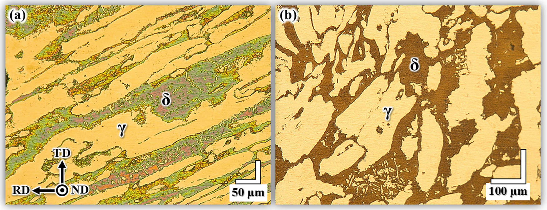
Optical micrograph of (a) as-received and (b) 20% cold-rolled duplex stainless steel microstructure. Arrows indicate microstructure processing orientation towards transverse direction (TD), rolling direction (RD) and normal direction (ND).
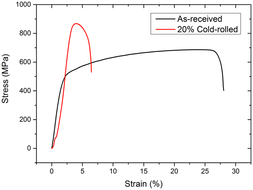
Stress–strain behaviour of as-received and 20% cold-rolled duplex stainless steel.
DIC of as-received microstructure
The results of the as-received microstructure after tensile straining to 0.04% and 0.8% macroscopic strain are shown in Figure 5. Small strain heterogeneities can already be seen after the application of 0.04% strain, primarily located in austenite regions. After further straining to 0.8%, most normal strain was still localised in austenite grains, but with more pronounced strain fields at some interphase boundaries.
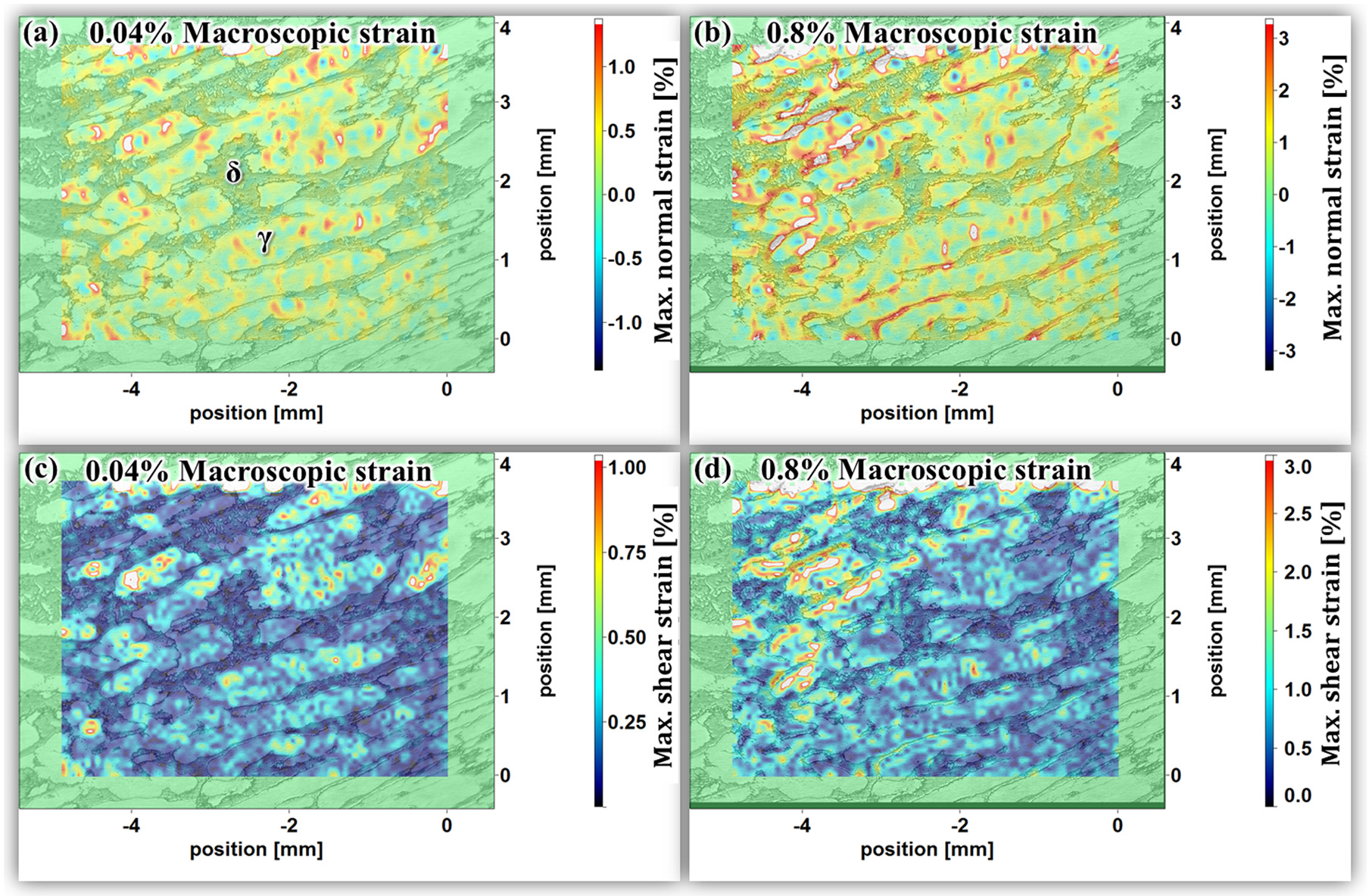
DIC analysis of the as-received microstructure with 0.04% and 0.8% macroscopic tensile strain with (a, b) showing maximum normal strain evolution with strain localisation in austenite and interphase regions and (c, d) showing maximum shear strain evolution concentrating primarily in austenite. Loading was applied to the horizontal axis of the images. Optical micrographs (400× magnification) of etched microstructure with KOH in normal direction. Interrogation window size: 32 × 32 pixels.
Figure 5(a) and (b) indicates that the strain distribution in the ferrite was far more homogeneous, while in the austenite and, to a lesser extent in certain regions, at interphase boundaries distinctive heterogeneous strain fields developed with increasing strain magnitude. El Bartali et al. 18 also reported heterogeneous strain fields at interphase boundaries, with the latter related to different crystallographic orientations of grains making up these interphases. There is often a strong Kurdjumov–Sachs orientation relationship existing in duplex stainless steels between the ferrite and austenite, in the form of [110](1–11)γ//[111](1–10)δ. This infers that slip transfer across interphases is facilitated if this orientation criterion is satisfied, leading to enhanced dislocation mobility. 19 However, intense heterogeneous strain fields can lead to micro-crack formation at sites where this orientation relationship does not exist, which can result in slip bands arresting at interphase boundaries. 18
Large crystallographic misorientations between neighbouring grains and the resulting slip system differences between both phases therefore limit dislocation motion. Strain localisation, in certain cases at least, can be indicative of stress localisation, and vice versa; hence intense heterogeneous strain fields can result in preferential corrosion as well as potential crack nucleation sites. In earlier work, it was shown that numerous heterogeneous strain fields at discrete regions, determined by local misorientation measurement using electron backscatter diffraction (EBSD), were found in cold-rolled grade 2205 duplex stainless steel microstructure, and such sites showed electrochemical activity with exposure to a chloride-containing atmospheric environment. 12
Some regions under compression or tension observed after 0.04% strain in Figure 5(a) were able to balance their strain fields after increasing the strain to 0.8%. Since tensile straining was incrementally performed, that is, after each straining step a time elapse was necessary to record an image of the microstructure, the material had time to creep, which may have affected the location of the small magnitude of normal strain locations in Figure 5(a).
Figure 5(c) and (d) shows that shear strain was localised in austenite regions, suggesting that shear deformation at interphase boundaries was less favoured than within the austenite grains. Austenite possesses 12 closely packed slip systems and allows easy dislocation mobility in almost all crystallographic directions while the ferrite possesses less closely packed slip systems, which typically possess higher critically resolved shear stresses for their activation. 4 The Peierls stress in the ferrite is typically higher than that in the austenite, rendering the austenite more ductile than ferrite. Therefore, plastic deformation of ferrite occurs usually after the first austenite grains have deformed, until the austenite is work-hardened.
The application of an additional +0.012% and +0.6% deformation in Figure 6, after changing to a higher magnification (1000×) to reach a maximum total applied strain of 1.4%, showed that the strain evolution became saturated or decelerated at interphase boundaries, while strain hardening of austenite continued, with in parallel the ferrite starting to accommodate larger strains. Strain hardening occurred preferentially in certain austenite grains indicating favoured grain orientation towards the loading direction. Both normal and shear strain indicated slip activity in the austenite, whereas only little strain activity was seen in the ferrite. This indicates that ferrite had a higher stiffness than austenite.
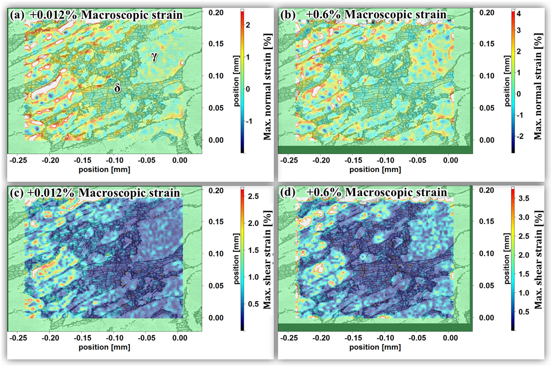
Higher resolution DIC analysis of the as-received microstructure with application of an additional 0.012% and 0.6% macroscopic tensile strain (in total 1.4% strain) with (a, b) showing maximum normal strain evolution and (c, d) showing maximum shear strain evolution. Loading was applied to the horizontal axis of the images. Optical micrographs recorded with 1000× magnification. Interrogation window size: 32 × 32 pixels.
Figure 7 shows the duplex microstructure after unloading and reloading the sample for SEM analysis to 0.024% and 6% macroscopic strain, showing intense heterogeneous strain fields with high strain gradients primarily in austenite grains and at a few ferrite-austenite interphase boundaries. The presence of discrete regions with tensile strain was typically accompanied by neighbouring regions with compressive strain fields. The extent of these compressive strain fields was larger than previously observed in Figure 6 due to the larger strain applied. Furthermore, the contrast of tensile and compressive regions was apparent, and the spacing between them was small, resulting in high strain gradients. This infers that un- and reloading caused further strain development with local strain re-distribution.
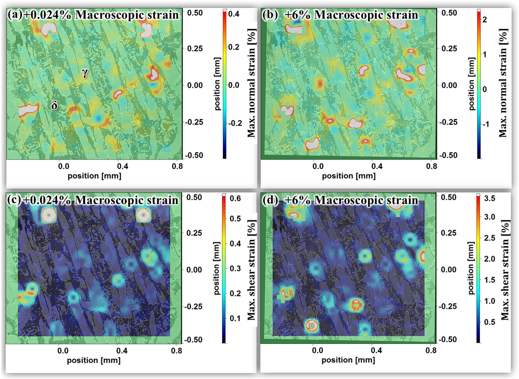
DIC analysis of the as-received microstructure with 0.024% and 6% macroscopic tensile strain highlighting with (a, b) showing maximum normal strain and (c, d) showing maximum shear strain. Loading was applied to the vertical axis of the images. Images were taken with an SEM at 500× magnification. Interrogation window size: 96 × 96 pixels.
Figure 7(c) and (d) shows that shear strain mainly developed in the austenite, with the maximum shear strain in certain regions larger than the maximum normal strain, suggesting that work-hardening had occurred due to shear deformation in the austenite. The presence of regions with compressive strain in austenite is most likely related to grains with less favoured orientation with respect to the loading direction. Adjacent grains with favoured orientation have possibly deformed, so that less favoured grains laying in-between deformed sites were compressed leading to the introduction of negative strains. Even after the introduction of 6% macroscopic strain, no distinct heterogeneous strain evolution in the ferrite was observed.
DIC of 20% cold-rolled microstructure
DIC results of the 20% cold-rolled microstructure after introduction of 0.012% and 4% macroscopic strain are shown in Figure 8. Heterogeneous strain concentrations appeared primarily in austenite and at interphase boundaries, both compressive and tensile in nature (Figure 8(a) and (b)). Compressive strain seemed to be related to the austenite, with ferrite showing no clear change up to 4% macroscopic strain. Discrete regions containing shear deformation were present in the austenite and at interphase boundaries at 0.012% macroscopic strain, and the ferrite seemed to accommodate more strain. Cold rolling clearly work-hardened the microstructure, and up to five times larger strain development in austenite was observed than in ferrite.
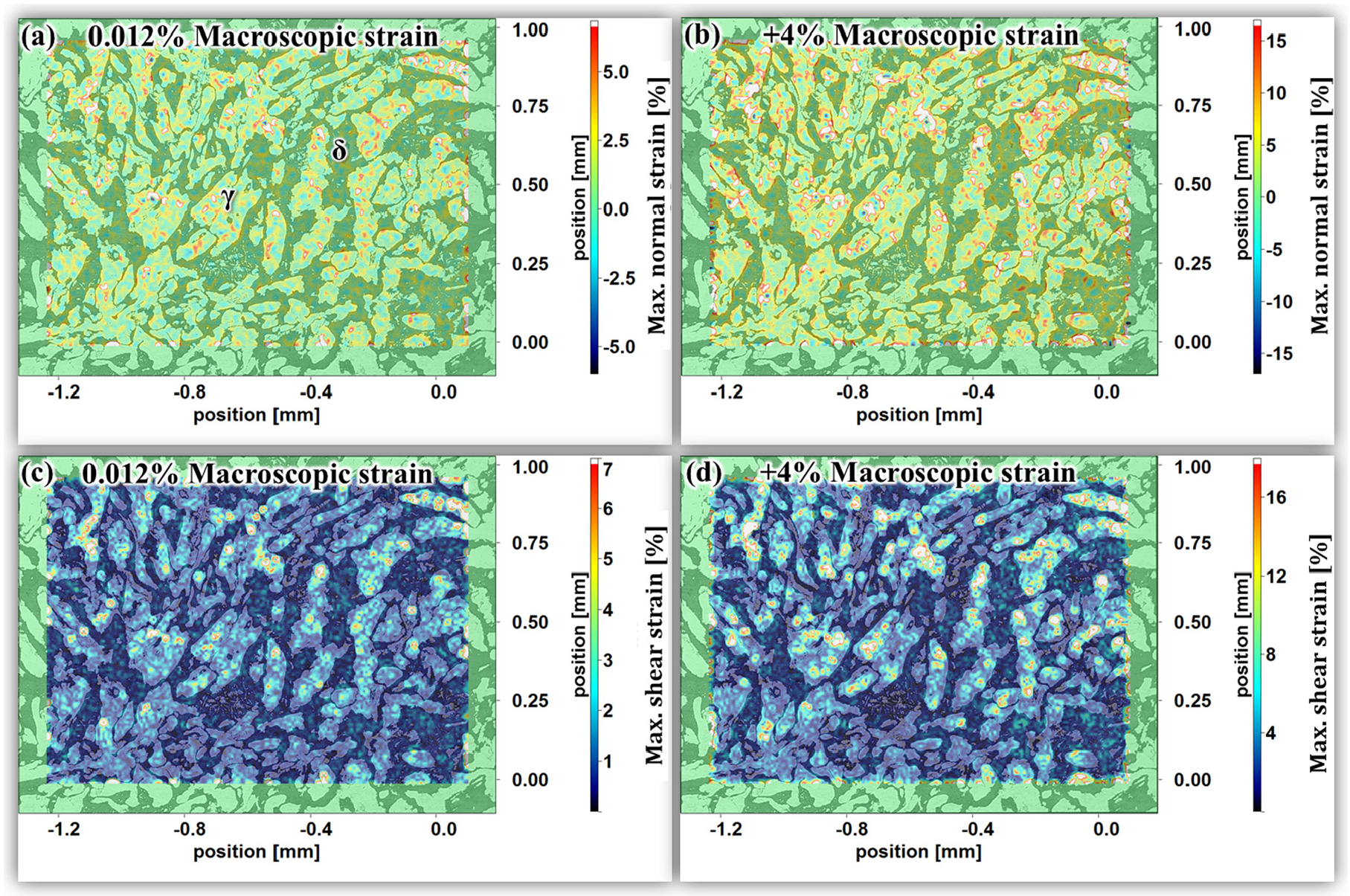
DIC analysis of the 20% cold-rolled microstructure after 0.012% and 4% total macroscopic strain with (a, b) showing maximum normal strain evolution and (c, d) showing maximum shear strain evolution. Mechanical loading direction was to the horizontal axis of the images. Optical micrographs recorded with 200× magnification. Interrogation window size: 16 × 16 pixels.
The strain heterogeneity was significantly increased in the cold-rolled microstructure compared to the as-received condition, and regions with high concentrations of tensile strain were observed in the vicinity of compressive strain fields. Higher resolution DIC analysis, shown in Figure 9, confirmed that large strain gradients exist within both phases. The strain distribution across the austenite was distinctively larger indicating more deformation occurred compared to the ferrite. The austenite in the cold-rolled microstructure was significantly strain-hardened and seemed to have accommodated additional strain by plastic deformation of the ferrite. Large heterogeneous strain fields also developed in ferrite and at interphase boundaries indicating a slip activity shift from highly strained austenite grains to neighbouring ferritic regions (Figure 9(c) and (d)).
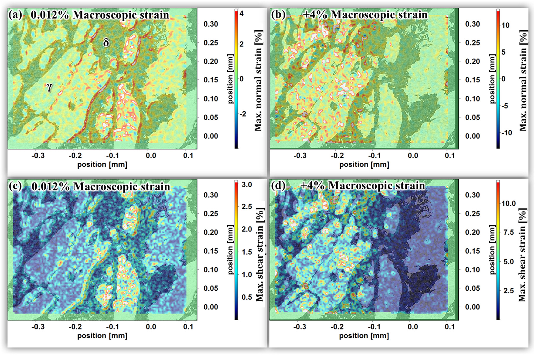
DIC analysis of the 20% cold-rolled microstructure after 0.012% and 4% total macroscopic strain with (a, b) showing maximum normal strain evolution and (c, d) showing maximum shear strain evolution. Mechanical loading direction was to the horizontal axis of the images. Optical micrographs recorded with 600× magnification. Interrogation window size: 24 × 24 pixels.
Summary of DIC observations
Strain hardening is primarily concentrated in the austenite phase in as-received microstructure due to much easier slip activity than in ferrite and lower stiffness. Most elastic and plastic strain is accommodated at certain regions in the austenite during mechanical loading as can be seen in Figure 10(a), showing the maximum strain intensities from DIC-processed images versus applied strain. Slip activity in ferrite is significantly lower than in austenite, and strain fields at the interphase boundaries are higher than in ferrite. However, strain fields developing in ferrite and at interphase regions quickly reach saturation enabling further strain hardening of the austenite phase.
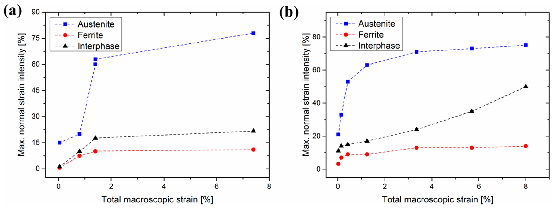
Maximum strain intensities of normal strain component measured in DIC mapped areas of (a) as-received and (b) 20% cold-rolled microstructures.
In the 20% cold-rolled microstructure, austenite was still accommodating most strain, with higher maximum normal strain intensities due to increasing strain concentrations and associated gradients as can be seen in Figure 10(b). The presence of discrete strain fields indicated accumulation of local deformation at confined regions. The ferrite and interphase regions showed accommodation of strain, which probably promoted slip activity in ferrite in the cold-rolled microstructure.
XRD surface stress determination
The quasi in situ XRD stress measurement results are summarised in Figure 11. Both ferrite and austenite contained compressive stresses in the as-received condition. Loading to 531 µ-strain (0.05%) indicated an increase of 150–170 MPa in both ferrite and austenite. The overall stress in ferrite became tensile, and the austenite became more balanced along the loading direction (phi = 0°). No clear change in residual stresses in the other direction (phi = 90°) was seen. Further loading to 1009 µ-strain (0.1%) strain showed stress development in both the ferrite (additional ∼220 MPa) and austenite (additional ∼120 MPa).
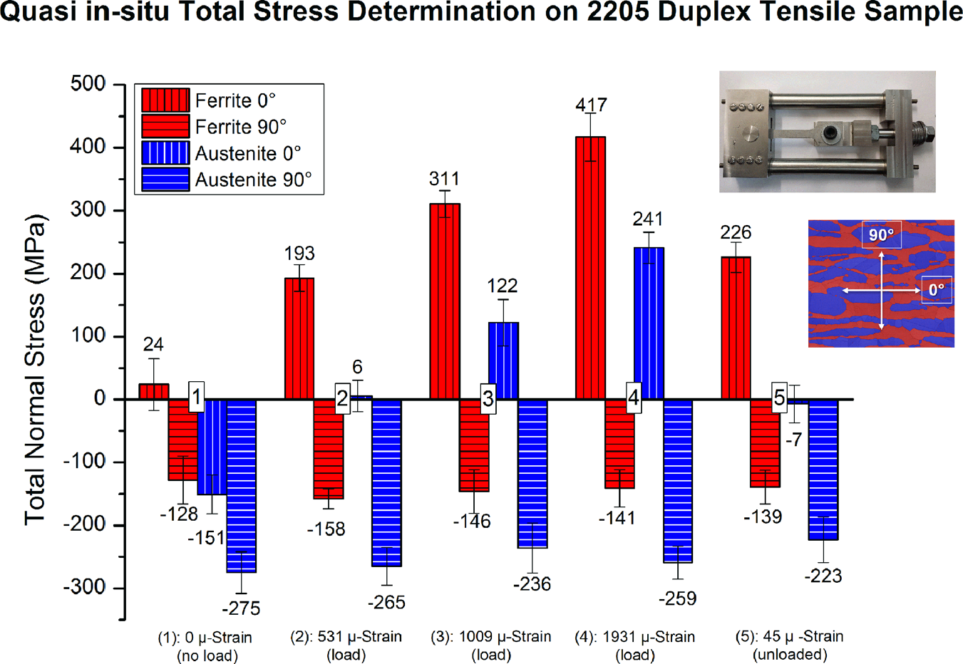
Quasi in situ XRD stress measurement of austenite and ferrite in the as-received duplex stainless steel microstructure.
Application of a final loading cycle to 1931 µ-strain (0.2%) strain increased the stress in both the ferrite and austenite by approximately 120 MPa. The increase in stress in ferrite and austenite along phi 0° seemed to be proportional in both phases with increasing applied load. With further increase in applied macroscopic strain, it is likely that the stress development in ferrite saturates earlier, ultimately resulting in the development of higher stresses in the austenite due to higher work hardening capability. Lower strains result in stress portioning to the ferrite. Therefore, strain localisation in microstructure does not necessarily lead to stress evolution at sites containing high strain in duplex stainless steel.
Unloading the sample revealed the presence of a residual stress in the ferrite (phi = 0°) of 226 MPa, with the austenite showing a reduction in the previously measured stress to a value close to 0 MPa. The FWHM values of ferrite and austenite as a function of macroscopic strain are compared in Figure 12. The FWHM of the austenite phase showed an overall increase compared to the ferrite, indicating the accommodation of more plastic strain in austenite with larger macroscopic deformations. The FWHM value is sensitive to the variation in microstructure and stress–strain accumulation in the material. Typically, an increase in stacking faults and structural disorders widens the XRD peaks, and the presence of tensile stress causes an increase in the FWHM, with relaxation processes typically decreasing its magnitude.20,21 After unloading, the FWHM of ferrite remained the same as the last straining step, whereas the FWHM increased in the austenite indicating accommodation of plastic strain in the austenite.
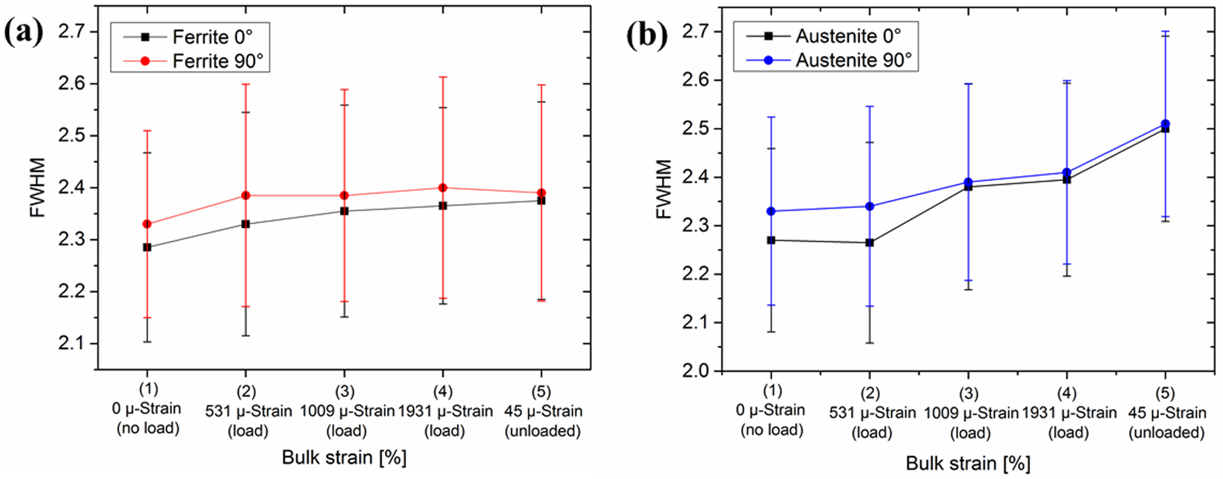
XRD FWHM values of (a) ferrite and (b) austenite of as-received microstructure as a function of total macroscopic strain.
SKPFM Volta potential measurements
Surface topography and SKPFM Volta potential maps of the as-received, 0.23% and ∼10% tensile strained microstructure are shown in Figure 13. The Volta potential distribution within the as-received microstructure was smooth in each crystallographic phase, with only long-ranged potential gradients. The austenite phase showed a Volta potential roughness (ΨRa) of 2.7 mV with a maximum potential variation of 21 mV across the entire phase, compared to a Volta potential roughness of ferrite of 3.6 mV with a maximum potential variation of 30 mV. A total Volta potential difference of 30 ± 15 mV was measured between ferrite and austenite, with the austenite having lower potential differences than ferrite indicating superior electrochemical properties. Volta potential correlation of ferrite and austenite regions with local electrochemical activity was earlier reported for 2205 duplex stainless steel. 12 Usually, the ferrite is preferentially attacked in chloride-containing environment, while the austenite is more corrosion resistant.11,12,22–25
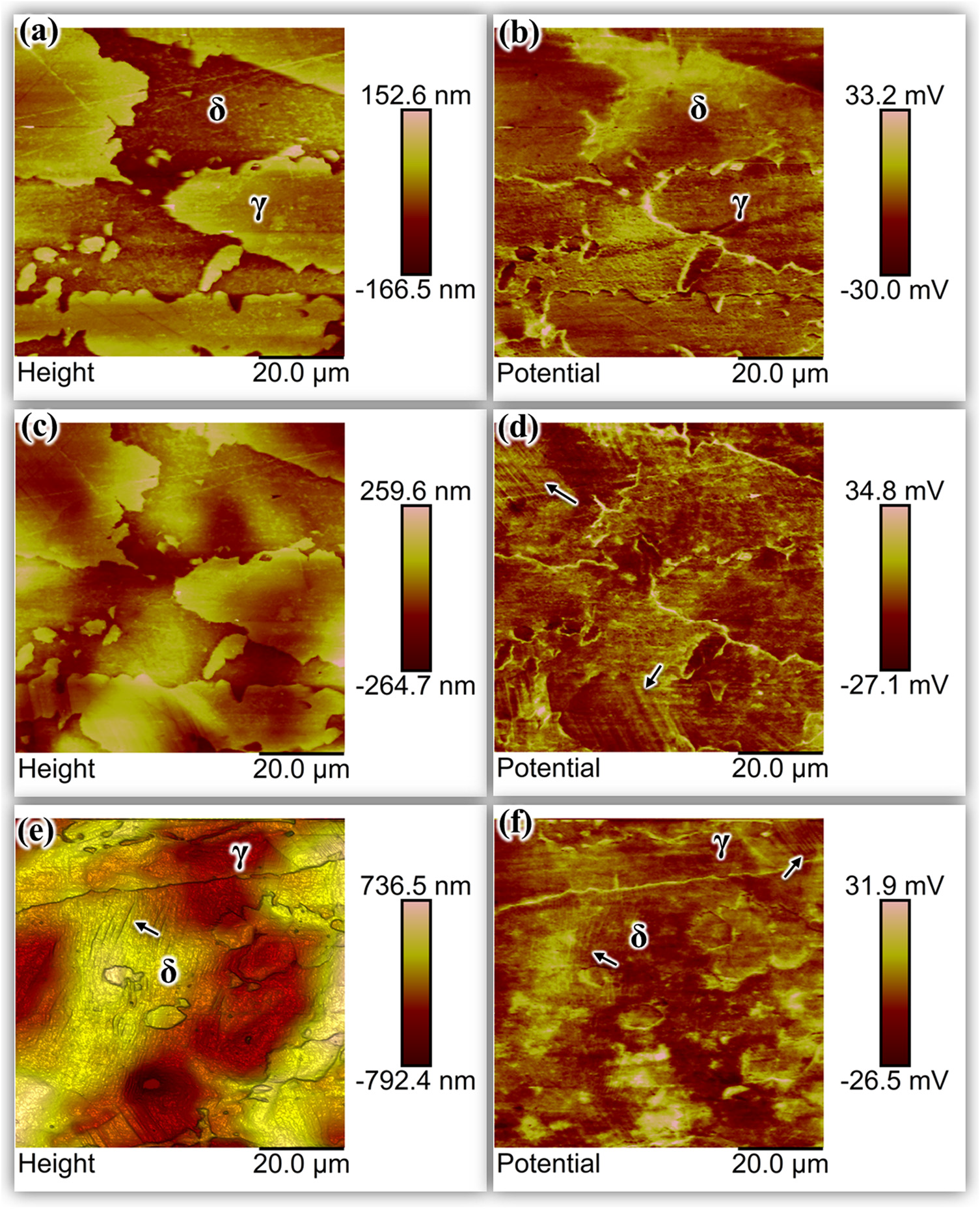
SKPFM Volta potential analysis after tensile straining with (a) showing the topography of as-received microstructure (normal direction view) with (b) showing the corresponding Volta potential differences map, (c, d) after 0.23% strain and (e, f) after ~10% plastic strain. Note that all potential maps were flattened to enhance potential contrast differences. Note that the arrows in the maps point at slip bands. Loading direction was oriented to the horizontal (rolling direction) of the images.
Volta potential differences between ferrite and austenite increased to 40 ± 30 mV after the application of 0.23% strain (in Figure 13(b)), with large scatter across the entire microstructure. The Volta potential roughness of ferrite and austenite increased to 4.1 and 5.4 mV, respectively, with potential variations of 32 mV for the ferrite and 33 mV for the austenite phase. This supports previous observations of changes occurring in the austenite and the ferrite after tensile straining, with reports of the development of discrete cathodic and anodic Volta potential sites at confined regions (hot-spots). The first slip bands were observed in the austenite, with Volta potential differences measured over slip bands having larger anodic character, in contrast to regions without slip band deformation. It is well known that the passive layer can be disrupted during plastic deformation processes, which typically generates a bare metal surface. Such sites can play a vital role in the initiation of corrosion processes.
Further plastic deformation to ≈10% total macroscopic strain enhanced the deformation activity in the bulk material, with more slip bands emerging primarily in the austenite, but also in the ferrite as shown in Figure 13(c). The Volta potential differences between ferrite and austenite decreased to 20 ± 15 mV. Austenite was on average slightly more cathodic than the ferrite by only 5 mV, indicating that plastic deformation decreased the Volta potential differences within the duplex microstructure. This would mean that a lower galvanic interactivity between ferrite and austenite is expected. Similar observation was reported after 40% cold rolling of 2205 duplex stainless steel. 12 Anodic and cathodic Volta potential fields at confined regions (hot-spots) with discrete geometries became more apparent indicating a possible driving force for local galvanic activity. Similar observation was also observed on copper, with an increase in dislocation density because plastic deformation was found to decrease the electron work function of copper, indicating enhanced electrochemical activity. 26
The Volta potential roughness parameter (ΨRa) increased to 5.8 mV for the austenite and 6.3 mV for the ferrite, with a maximum potential variation in each phase further of 35 and 43 mV for austenite and ferrite, respectively. This indicates heterogeneous Volta potential sites in each phase, promoting local galvanic activity. The Volta potential roughness and maximum Volta potential variation in ferrite and austenite as a function of tensile strain are summarised in Figure 14. Here, the effect of applied strain on the changes in Volta potential differences of ferrite and austenite becomes clearer, indicating initially small changes in the ferrite, accompanied by larger potential changes in the austenite. This is in line with DIC observations of strain localisation at interfaces and austenite, followed by the ferrite taking up more strain. The latter seems to affect the Volta potential differences as well, as summarised in Figure 14.
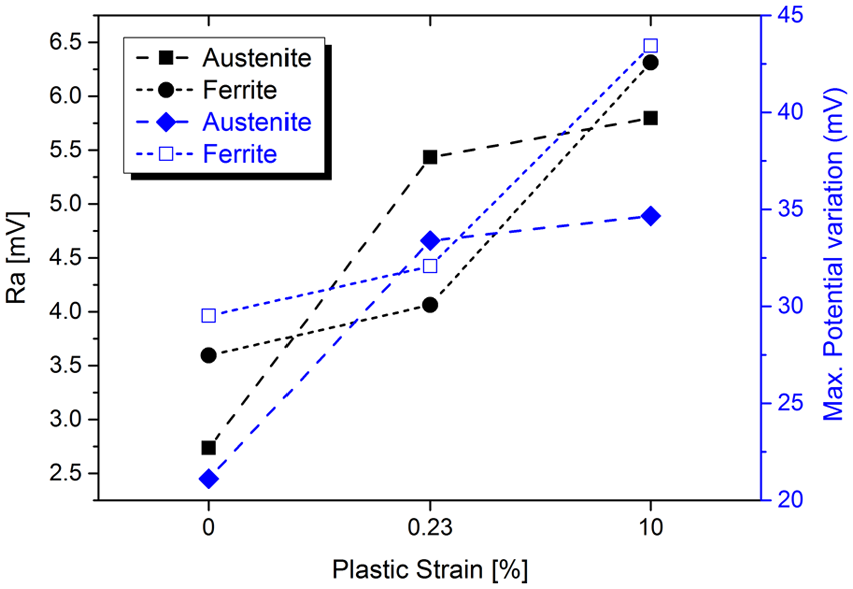
SKPFM analysis of Volta potential roughness (Ra) values with maximum potential variation.
Conclusion
Strain partitioning with Volta potential development in 2205 duplex stainless steel has been analysed and can be summarised as follows:
DIC analysis of quasi in situ strained micro-tensile specimens showed local strain development primarily in the austenite. Discrete heterogeneous strain fields within austenite grains indicated higher work-hardening behaviour and lower stiffness of austenite than ferrite.
Work-hardening of the austenite enabled the ferrite to accommodate more plastic strains which led to the evolution of heterogeneous strain fields within ferrite regions.
XRD stress measurements showed that strain localisation does not necessarily indicate stress localisation; ferrite showed almost double the stress than austenite during quasi in situ straining to 0.2% macroscopic strain.
SKPFM Volta potential measurements showed reduced Volta potential differences between ferrite and austenite with the introduction of macroscopic deformation.
The introduction of tensile strain increased the Volta potential roughness (ΨRa) and the maximum potential variation across ferrite and austenite phases, leading to the development of discrete cathodic and anodic Volta potential sites.
Footnotes
Acknowledgements
The authors are grateful for the kind provision of grade 2205 duplex stainless steel plate by Rolled Alloys (UK). Mr Gary Harrison, University of Manchester, is thanked for his support during XRD stress measurements.
Declaration of conflicting interests
The author(s) declared no potential conflicts of interest with respect to the research, authorship and/or publication of this article.
Funding
The author(s) disclosed receipt of the following financial support for the research, authorship, and/or publication of this article: The authors acknowledge Radioactive Waste Management (RWM) (NPO004411A-EPS02) and EPSRC (EP/I036397/1) for financial support.