
Abstract
Medium or high-entropy alloys have led to widespread interest in their preparation, property control, and applications. The ability to apply these new alloys as coatings on conventional materials allows alternative surface treatment methods. This study used electrospark deposition with powder feedstock, to form MEA coating with fine-tuned compositions on steel substrate. Single-phase CrFeCoNi MEA using optimized ESD parameters and powder formulation. The phase and composition of MEA coatings and their hardness were also characterized. The coating showed two orders of magnitude reduction in specific wear rate coefficient compared with that of bare A516 steel substrate. This study demonstrates that the powder-based ESD technique can be used to create in-situ M/HEA coatings for applications requiring improved properties.
Introduction
High entropy alloys (HEAs) contain 5 or more principal elements with atomic fractions between 5% and 35%, 1 often having highly disordered atomic arrangements and forming stable solid solutions at high temperatures. This disorder can increase their stability and beneficial properties, including slow diffusion rates due to the random and non-uniform local energies, and high solid solution strengthening due to the increased lattice distortion that impedes dislocation movement. 2 A class of medium entropy alloys (MEAs) with less configurational entropy are also of interest due to their comparable properties with that of HEAs. The elemental combinations of M/HEAs have high diversity, where the 3d transition metal HEAs are most widely studied, such as AlCrFeCoNi, CrMnFeCoNi, etc., 3 which have superior fracture toughness, 4 yield strength, and specific strength. 5
To utilize the superior properties of these M/HEAs in engineering, the coating is one of the main applications to improve the properties, such as resistance to wear and corrosion, of conventional alloys workpieces. For example, RhRuPtPdIr thin film was fabricated on glassy carbon electrode substrate using atomic layer deposition which exhibits excellent hydrogen evolution reaction. 6 Magnetron sputtering was used to deposit CrFeCoNi on MgO crystal substrate which shows deposition quality. 7 AlCrFeCoNi coatings have been fabricated on 316L stainless steel substrate through plasma spraying with high-purity single-element powders, 8 pre-synthesized CrMnFeCoNi HEA powder was applied onto 2024 aluminium alloy with cold spraying. 9 Laser cladding was also used to coat Al0.6CrFeCoNi HEA on Q235 steel with a single-element powder mixture. 10 These studies all use powdered materials as feedstock. However, these powders require specific sizes and shapes, and the process parameters needed for high-quality coatings and bonding are complex, making manufacturing expensive. Hence, there is a need to explore simpler and more intuitive coating techniques.
Electrospark electrode deposition (ESED) process, a low-energy welding technique, typically uses a rod electrode to form the coating by generating sparks when the rotating electrode and substrate come into contact. Instead of the direct deposition of electrode materials on the substrate, the powder materials can also be used as the feedstock to achieve coating with ESED, which is known as electrospark powder deposition (ESPD). Zhao et al. 11 used a NiCrSiB powder-covered electrode to deposit metal matrix composites (MMC). Recently, electrospark was adopted for alloying Ti-Ni-Zr-Mo-Al-C composite coating on Ti-6Al-4 V surface for higher resistance to wear and high-temperature gas corrosion using metal/alloy powders Ti, Ni, Zr, Mo, Al and Ti3Al + 10%C mixture. 12 These investigations suggest that powders can be one of the feedstocks in coating fabrication, and the “straightforward” combination of M/HEA coatings can be fabricated with ESPD, which could largely simplify the coating process and is readily for new alloy development, yet there is no study related to this approach. In addition to this manufacturing process, the ESPD can rapidly fabricate the M/HEA coating using conventional metal or alloy powder, which can largely reduce the cost, it can neglect the complex surface morphology of the substrate, and it has low requirements to the feedstock in terms of size and shape. The ESPD technique generally exhibits a lower deposition rate compared to other coating methods, making it more suitable for thin coatings. However, one of the key advantages of ESPD is its localized heating with minimal heat input to the substrate. 13 In contrast, methods such as laser cladding and plasma spraying involve significant heat input to both the substrate and the powder feedstock, which can result in oxidation and alteration of their properties. Additionally, ESPD forms a strong metallurgical bond between the coating and the substrate, ensuring excellent adhesion and durability. 13 Conversely, the bonding strength of cold spray coatings may be lower due to their reliance on plastic deformation and interlocking mechanisms. Furthermore, ESPD allows for precise coating of small and intricate areas, whereas spray techniques are generally more suitable for large-area coatings. 13
This study fabricates a CrFeCoNi MEA coating on A516 steel via ESPD process using Cr, Fe, Co, Ni powder mixtures. The deposition parameters, such as electrical parameters and powder mole fraction, are optimized to reach the desired composition in the MEA coating. The microstructure, microhardness, and the wear property of the coatings will be characterized. This study will explore the feasibility of manufacturing H/MEAs coatings using ESPD with powder as the raw material.
Materials and methods
Experimental materials
Commercially available high-purity (>99.8%) Cr, Fe, Co, and Ni powders (Thermo Fisher Scientific) with non-uniform shapes shown in Figure 1(a)-(d) were used as feedstock, the sizes of the powders are varied from 4 to 40 μm, the non-uniformed sizes can ensure the occupation of the space of the mixture, which is also studied in additive manufacturing process. 14 During the deposition process, a slurry-like powder mixture was used for this study to reduce dry powder movement due to the rotating electrode and flowing gas cover. The four metal powders were mixed according to the equal mole fraction of each element in the MEA. The ratio of mixed powder: polyvinyl alcohol solution (PVA, 10 wt.% aqueous): ethylene glycol (EG) was 12g:1mL:1.4 mL to form a slurry. The slurry was applied onto a 1.76 mm thick A516 plate and then dried on a hot plate. The morphology of the slurry after drying is shown in Figure 1(e). Although the morphology of the powders differs, the influence of these characteristics on the process is not within the scope of this study.
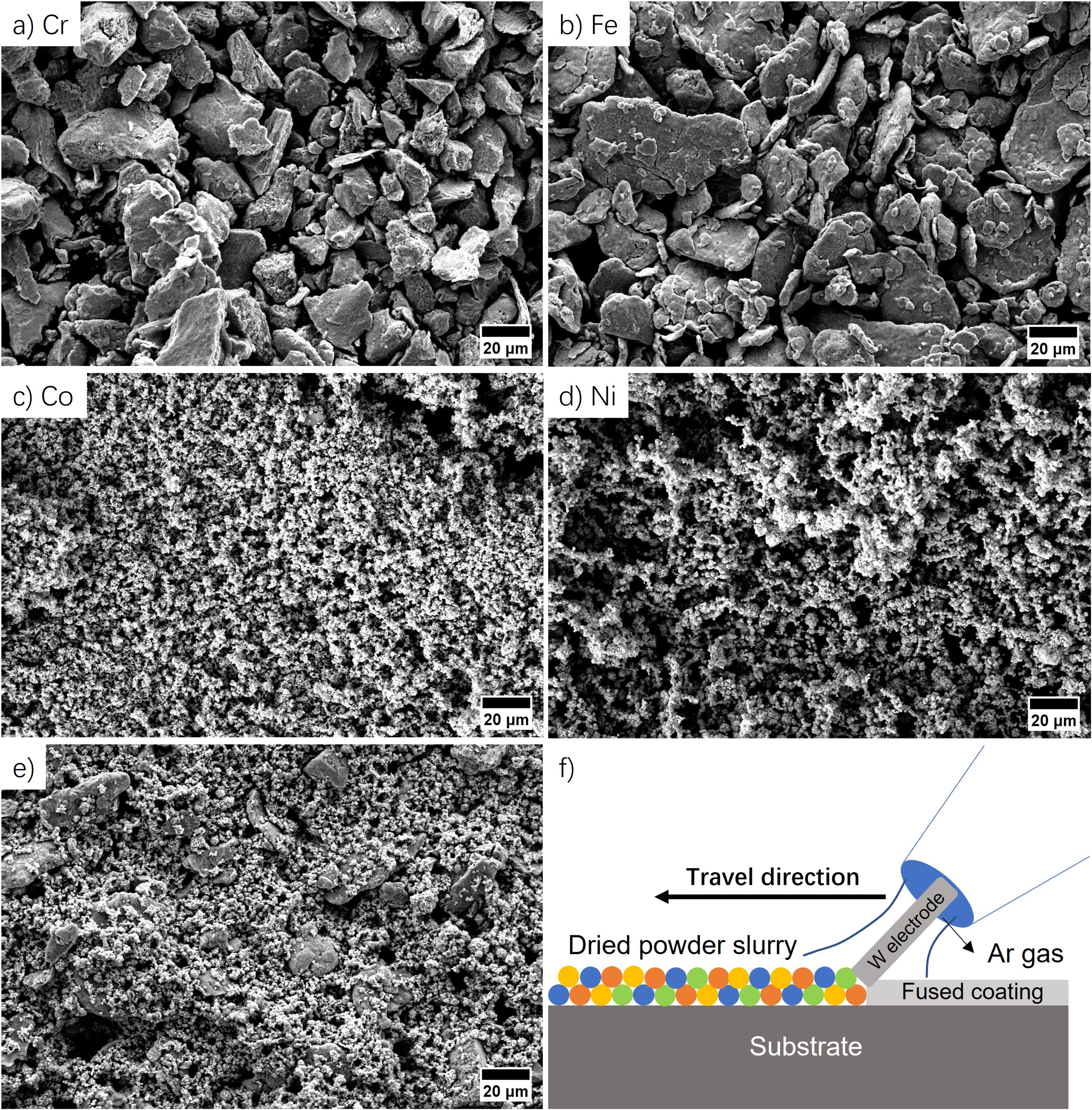
Morphology of powder feedstock a) Cr; b) Fe; c) Co; d) Ni; and e) dried slurry; f) a brief sketch of ESPD.
Electrospark powder deposition (ESPD) process
The process of the ESPD is sketched in Figure 1(f). A pure tungsten rod with 3.175 mm in diameter was used as the electrode to restrict the unexpected addition of the electrode material into the coating. The electrode was moved along sketched direction while contacting and fusing the powders to coating. The process parameters adjusted in this study to create the alloy coating are capacitance, voltage, and pulse frequency, with the ranges shown in Table 1, after the preliminary experiment. A manual ESD machine manufactured by Huys Industries was used with a 20 L/min flow of argon shielding gas to minimize the oxidation of the powder.
Electric parameters attempted for powder deposition using ESD
The pulse energy (E) and power input (P) during the ESD were calculated using equation (1) and (2).

Characterization
The coated/uncoated samples were mounted in conductive resin and were ground and polished. The steel substrate was etched with Nital etchant for microstructure characterization, and Kalling's 2 Reagent was used for the analysis of the alloy coating microstructure. Microhardness was measured by a microhardness tester (CMT (v. 8.0.197), Clemex, Canada) with a force load of 25 g and a dwell time of 10 s. A linear wear tester with a 4 mm diameter ZrO2 ceramic round pin was used to perform the abrasive wear test with a force load of 988.9 g for 200 cycles (400 passes) with 7 mm of travel distance per pass. Roughness was measured with an optical profiler (NT1100, WYKO, USA) and a laser profilometer (VK-X250, Keyence, Canada).
The macro-scale and detailed microstructure were analyzed by an optical microscopy (BX51 M, Olympus, Japan) and a field emission scanning electron microscope (SEM) (UltraPlus, Zeiss, Germany) with an energy-dispersive X-ray spectroscope (EDX) (Apollo XL, AMETEK EDAX, USA) attachment for element information. X-rays diffraction (XRD) (Materials Research Diffractometer (MRD), PANalytical, Netherland) spectra were obtained with copper being anode material, X-ray wavelength of 1.5406 Å. The electron backscattered diffraction (EBSD) (7000F SEM, JEOL, Japan) was performed in the Canadian Centre for Electron Microscopy (CCEM), and the obtained results were post-processed using HKL channel 5 software.
Results and discussion
Deposition parameter study
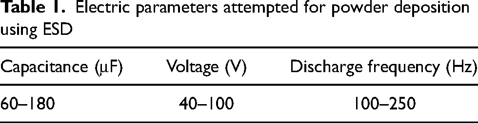
The conventional principle of ESED is the generation of sparks when the anode and cathode come into contact, resulting in a very high local temperature that causes the anode electrode material to melt, transfer, and solidify onto the substrate. 16 Similarly, when ESED is performed with powders, the powder particle in contact with the cathode substrate can be considered as the cathode during the powder deposition process. The high temperatures during the spark cause the powders to melt, fuse together, and solidify onto the substrate to form coating. In the ESPD process, when the electrode contacts with the dried powder slurry, the sparks are generated immediately. The slurry that has dark, rough, non-reflective surface starts burning, and transfer to a layer coating that has of silver, bright, and continuous surface. The 3 most typical characterizations are shown in Figure 2. A cross-sectional image of the coating deposited with the ESPD parameter set of 100 μF, 60 V, 100 Hz, which corresponds to a relative low pulse energy of 0.18 J and power input of 18 W, is shown in Figure 2(a), where most of the powders are fuse, but some unmelted particles are still visible. EDX analysis shows that these are mainly unmelted Co and Ni powders located between a fused layer of powder and the substrate, which may due to the low parameter set, the voltage is not high enough to overcome the small gaps between the particles to melt and mix the powders, in the image case, the Co and Ni powders, which can be observed in almost all the parameter sets with low energy input. This is expected to be highly detrimental to the integrity of the coating, which suggests that the increasing pulse energy and power input is needed to ensure a greater melting. When the parameters are increased to 180 μF, 100 V, 250 Hz, corresponding to high pulse energy and power input of 0.9 J and 225 W, respectively, the powders are completely fused whereas tungsten could also be deposited from the electrode as shown in Figure 2(b). EDX analysis shows the weight fraction of the W was 63.13% because of excessively high pulse energy, and the higher the energy input, the more the electrode material deposited. Therefore, a medium parameter set of 150 μF, 70 V, and 200 Hz was selected for powder deposition for detailed study, and the EDX mapping analysis with this parameter set is shown in Figure 2(c) shows an even distribution of elements in the coating and unmelted Cr powder. The influence of the characteristics of the powders on the coating quality did not show any impact to the deposited coating in Figure 2(c), but a study on comparison of powder morphology needs to be performed for optimization of coating fabrication, whereas this is not in the focus of this study.
SEM image of a) partially molten powder mixture with its magnified area at low pulse energy and power input; b) undesired W inclusion at high pulse energy and power input; c) fabricated coating with selected parameter set and its EDX mapping.
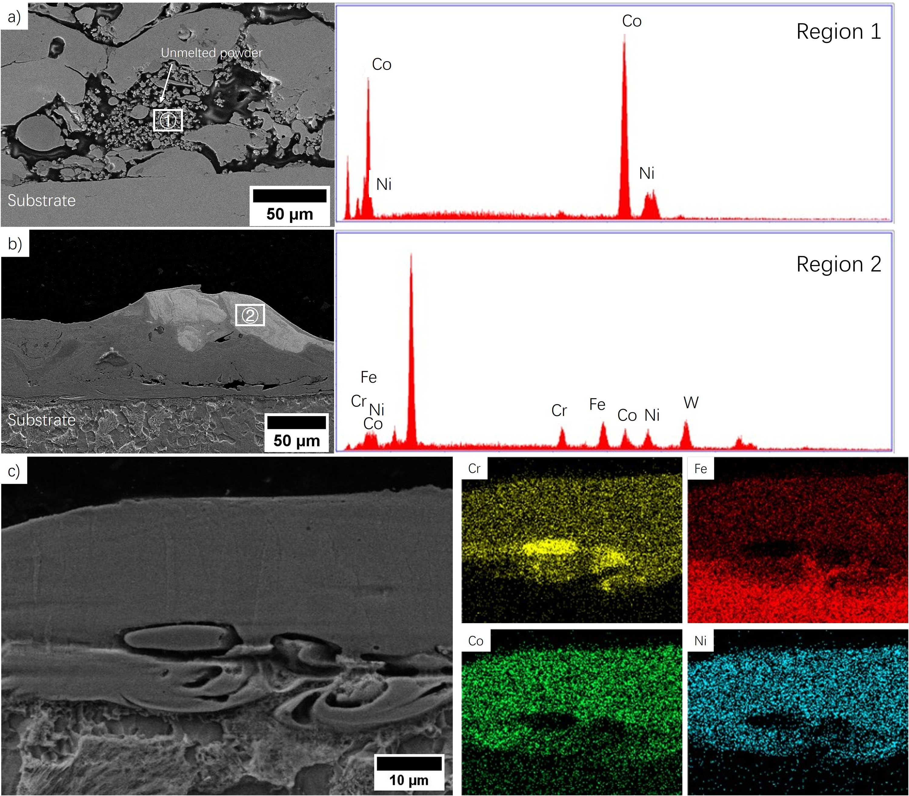
The Cr, Fe, Co, and Ni powder slurry with a mole fraction of 1:1:1:1 for the constituent elements is used for MEA coating fabrication. The cross-section of the as-deposited coating is shown in Figure 3(a). The EDX line scan in Figure 3(b) indicates the coating is nearly equiatomic. A gradual increase in the atomic fraction of Fe near the coating-substrate interface is due to the dilution of Fe from the substrate, and the slight change of Cr is because of the incomplete melting during the deposition processes.
a) Cross-section and b) EDX analysis of deposited equiatomic coating with Cr, Fe, Co, Ni powder slurry mixture. XRD analysis of c) A516 steel substrate and d) the deposited coating.
The XRD spectra of the A516 steel and the deposited coating are shown in Figure 3(c) and (d), respectively. The A516 substrate has a BCC phase whereas the coating has the FCC phase. Three peaks corresponding to (111), (200), and (220) plane, respectively, can be observed. The lattice constant of the deposited alloy is calculated to be 0.358 nm, which agrees with the CrFeCoNi alloy fabricated with laser melting 17 and arc melting methods. 18
Deposition process optimization
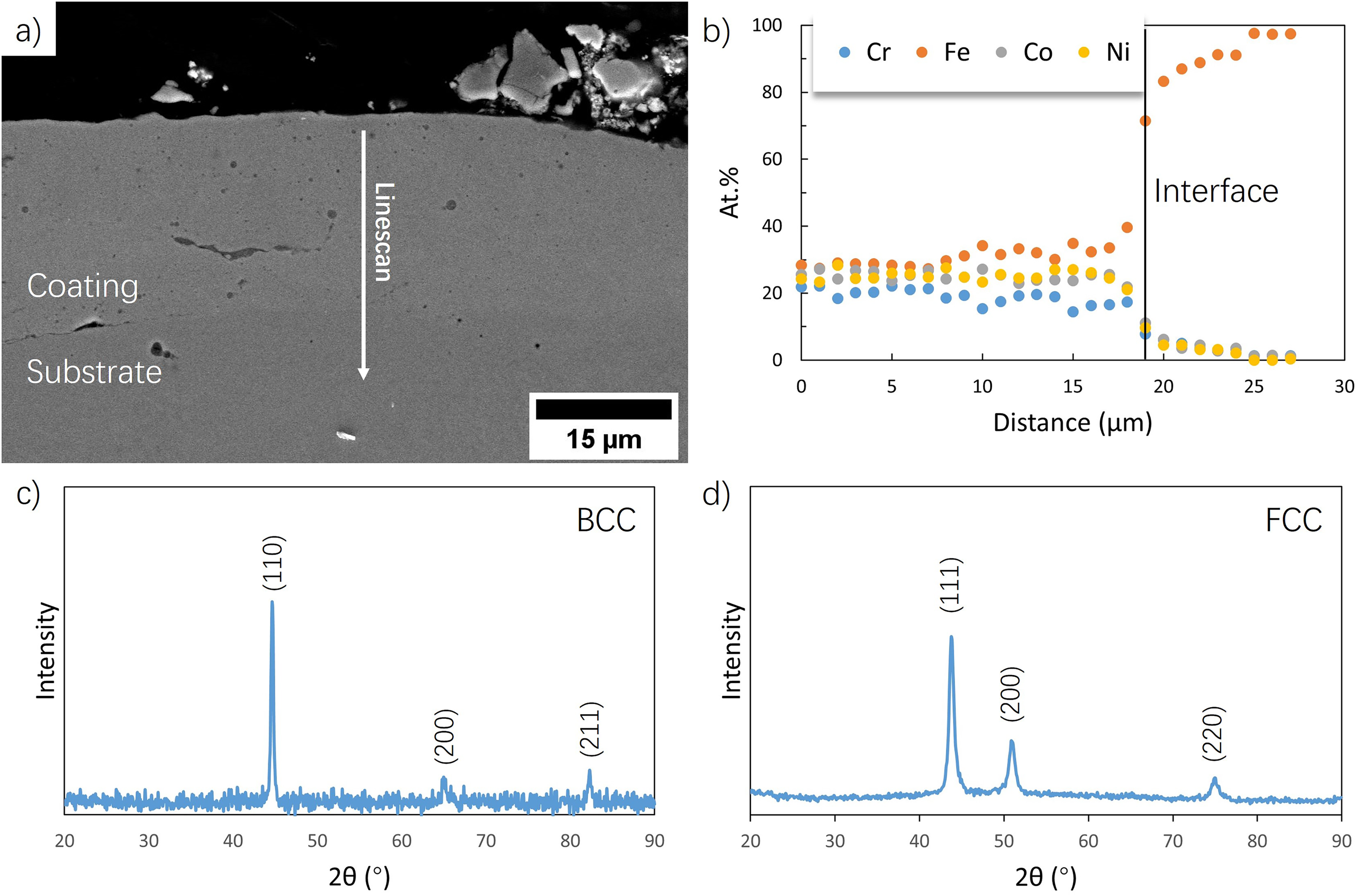
With the most appropriate parameter set, the deposition process can also be optimized, which can combine the ESPD and ESED in the entire deposition process (dual deposition process). When deposition is performed directly with electrodes (ESED), the electrode material melts and rapidly solidifies onto the substrate surface. For ESPD, the powders act as an intermediate between the electrode and substrate. The poor electrical connection between the powders and the substrate would cause the melted powders to be deposited on the electrode as well, see Figure 4(a). The EDX analysis (Figure 4(b)) indicates the deposition on the electrode yields an atomic fraction of 24.55%, 24.84%, 26.87%, and 23.73% for Cr, Fe, Co, and Ni, similar to the coating composition on the substrate. This suggests MEA is also deposited on the W electrode. Consequently, post surface smoothing process was then performed with this MEA coated W electrode using low pulse energy conditions to smoothen the deposited coating on the substrate. Although low pulse energy decreases the deposition rate,15,19 re-melting/depositing the MEA alloy on the electrode to the valleys for smoothening the substrate surface can happen. In the study, the parameter set of 60 μF, 40 V, 100 Hz was used for surface smoothening. Figure 4(c)-(f) show the surface morphology and roughness of coating before and after smoothening. The arithmetical mean height (Ra) within the effective measurement area is 17.86 μm, while the distance between the peak and the valley (Rz) is 127.73 μm. A significant improvement in roughness after low-pulse-energy smoothing is observed, with a decrease in Ra and of Rz 11.61 μm and 83.23 μm, respectively.
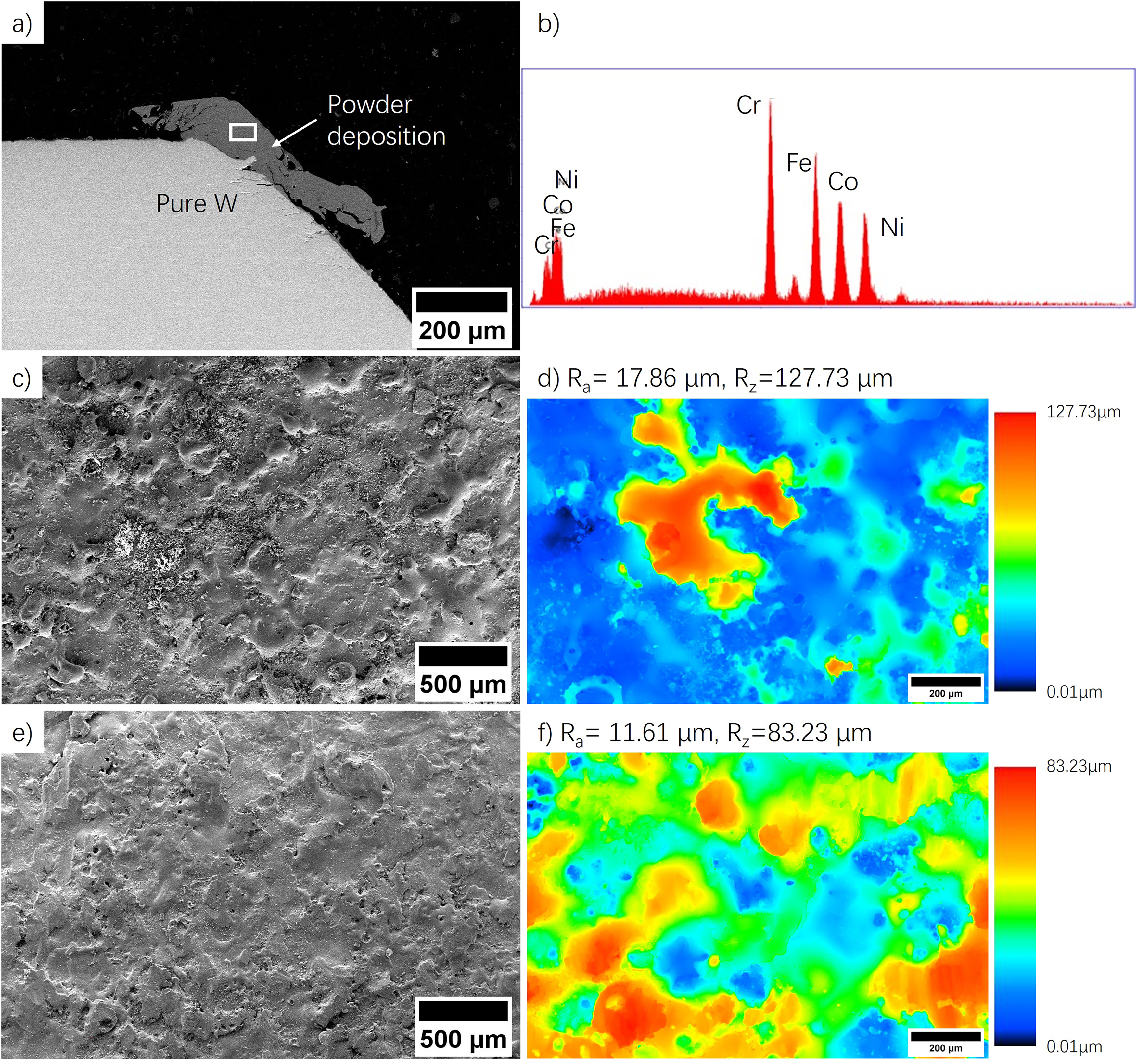
a) SEM image of W electrode after deposition with powder deposited on the electrode; b) the EDX analysis of deposited alloy; c) SEM image of the as-deposited coating surface with high pulse energy and d) its roughness measurement; e) smoothened surface with deposition of alloy on the electrode under low pulse energy and f) its roughness measurement.
Microstructure and microhardness of the in-situ MEA coating
The OM images of the coating after etching are shown in Figure 5(a) and (b). Columnar grains parallel to the deposition direction can be observed due to the epitaxial growth.20,21 OM image of the coating after major etching are shown in Figure 5(c). SEM image at the same area is shown in Figure 5(d). EDX mapping shows a homogeneous coating that has an even distribution of elements and no obvious segregation of elements between different grains. No W was detected in the overall regions, suggesting the melting of W is negligible in the process. A Fe-rich zone in the coating near the interface can be observed, which shows the dilution of the substrate.
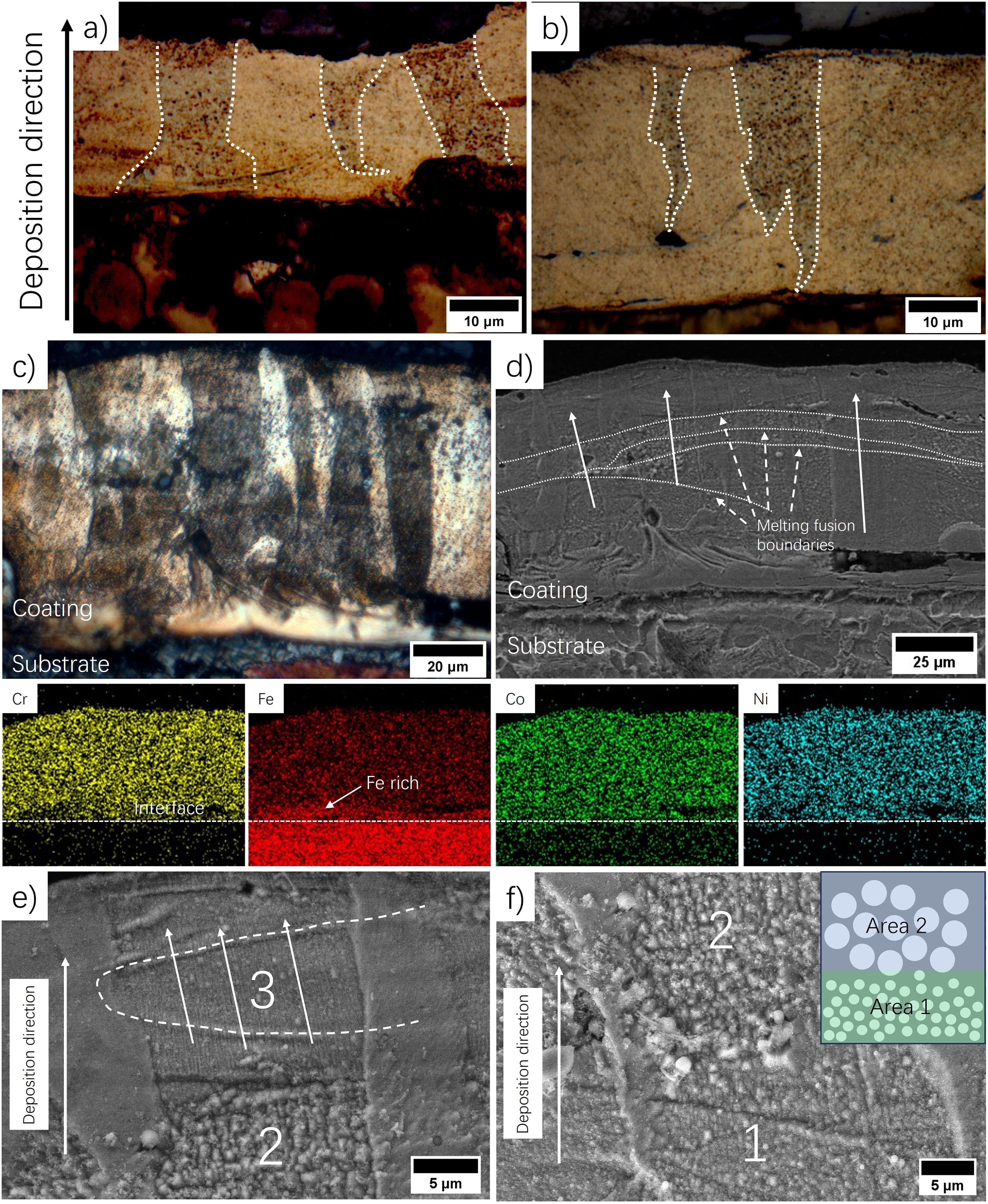
a) and b) OM images of minor etched coating. c) OM image of the major etched region; d) SEM image at the same region with EDX mapping; e) and f) representative magnified areas in a) with a texture sketch.
The boundaries between the different deposited passes can be observed and are marked in Figure 5(d). The grains extend from the substrate to the top of the coating indicated by arrows that penetrate throughout multiple fusion lines, this is because the atoms in the liquid (melted material) stick on the solidified materials and arrange themselves with the same atomic pattern, thus they do not change the orientation of crystallization.20,21 Three regions with different microstructures are represented with numbers in Figure 5e and f. With the melt pool highlighted with dash line in Figure 5(e), region 3 is considered as the ESED layer with material splat. 15 Region 1 and 2 represent the ESPD layer which does not have the splashing structure. Region 2 has a coarser granular texture size of 1–2 μm, and those of the texture in region 1 are <1 μm, which suggests ESED involves a relatively higher or more effective heat input, which can coarsen the texture of the deposited layer. In addition, the heat input of ESPD is not high enough to coarsen the deposited ESED layer, resulting in the texture size in region 1 being evidently smaller.
EBSD results of the coatings are shown in Figure 6. The substrate and coating have the iron BCC phase and the FCC phase, respectively, as shown in Figure 6(a). The equiaxed grains can be observed in the substrate in Figure 6b, while the coating has columnar grains, which is consistent with the OM and SEM observations. The grain size of the steel substrate near the interface is smaller than that in the bulk region, which is because the materials in this region are formed through recrystallization during the melting and solidification process, which can also be observed in Kernel average misorientation (KAM) map in Figure 6(c), with a relatively higher misorientation near the interface. An unindexed layer can be observed near the interface between the substrate and the coating, which might be due to the formation of nano-sized grains or residual stresses with the dilution of substrate elements. Therefore, the Kikuchi pattern at the interface is not able to be indexed with the selected phases (iron BCC and Ni-superalloy FCC phases). In addition, the intermetallic compounds formation at the interface could also result in the unindexed region.
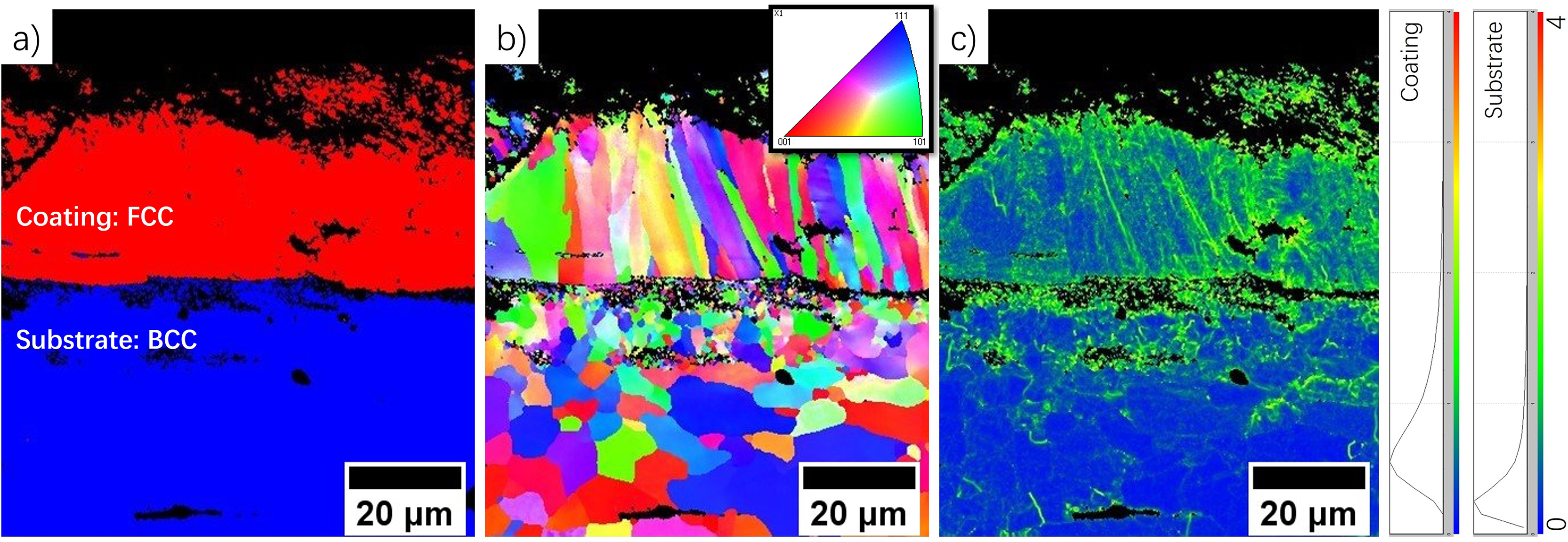
EBSD analysis of deposition with a) phase map; b) IPF X map, and c) KAM map.
Heat-affected zone in A516 carbon steel
The microstructure of the as-received A516 carbon steel substrate is shown in Figure 7a. A ferritic microstructure is observed and the measured microhardness of the as-received A516 steel is 186.0 ± 3.5 HV. Small changes in terms of the phases and size of the grains are observed after the ESPD process, as shown in Figure 7(b). This is attributed to the low-energy input that occurs during ESPD, with minimal heating of the substrate. The microhardness measured on the coating is 331.5 ± 18.9 HV, which is much higher than that of the cast22,23 and arc melted 24 CrFeCoNi MEA with a much lower grain width of approximately 7 μm as shown in Figure 7(b). Therefore, the relatively high hardness can be attributed to the finer grain size, and the width of the texture may also play an important role in determining the microhardness15,25 and possibly high residual stresses caused by very high cooling rates in ESED process. 18
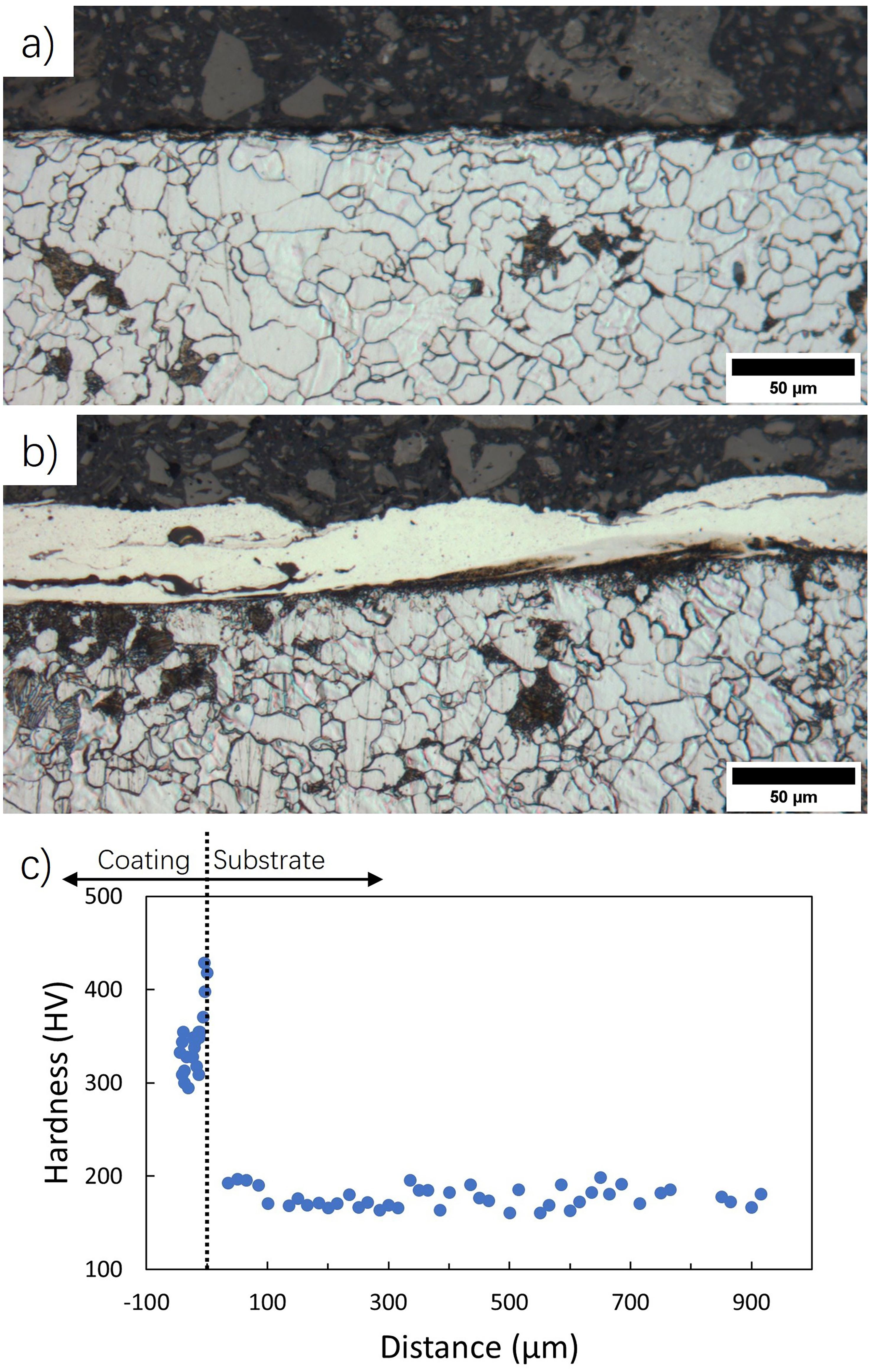
Om images of microstructure of a) A516 carbon steel substrate without and b) with coating; c) microhardness profile of coated sample on the substrate.
Figure 7(c) shows the microhardness profile of the coating (negative) and substrate (positive). The microhardness of the interface (distance = 0) is much higher than the A516 steel and the deposited CrFeCoNi. This might be attributed to the dilution of Fe from the substrate and the resulting IMCs formation, as mentioned above.
Wear property of coatings
Figure 8(a) and (b) show the microstructure of bare A516 carbon steel surface after wear test. The depth measurement is shown in Figure 8(c), where the X and Y axes are marked, and the Y represents the direction of the wear test. The height profiles at typical cross-sections (Y) are shown in Figure 8(d), showing that the width and depth of the wear track are approximately 0.78 mm and 11.5 μm, respectively. Figure 8(e) and (f) show the wear test track on the surface of the MEA-coated sample, exhibiting a narrower and shallower track. The depth measurement and height profile in Figure 8g and h indicate the average width and depth of tracks are approximately 0.16 mm and 2.5 µm, which is significantly lower than that of bare steel.
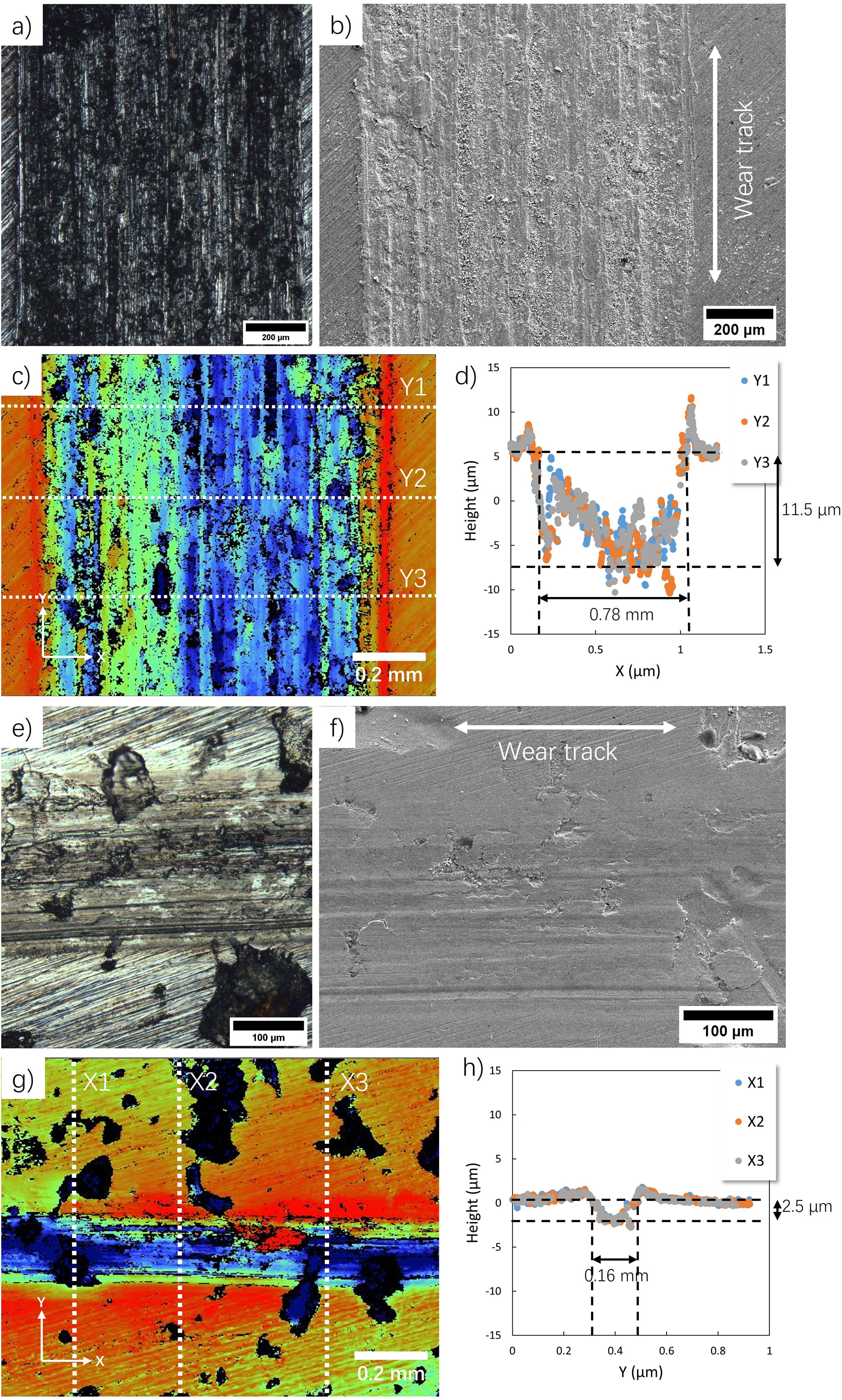
a) OM image and b) SEM image of linear wear track on the A516 steel substrate surface; c) depth measurement of the wear track and d) its height profile at random cross-sections (Y); e) OM image and f) SEM image of linear wear track on coating surface; g) depth measurement of the wear track and h) its height profile at random cross-sections (X).
The specific wear rate coefficient can be calculated using equation (3).
Conclusions
This study produced a high-quality equiatomic MEA CrFeCoNi coating by depositing an elemental powder mixture slurry using ESPD technology. A dual deposition process (ESPD + ESED) can evidently smoothen the coating. The microhardness of the coating was measured as 331.5 ± 18.9 HV, with columnar grains along the deposition direction. The minimum HAZ after ESPD was observed because of the low heat input nature of ESD. The CrFeCoNi alloy coating exhibited higher wear resistance than the steel substrate, which provides 95.56% reduction in the specific wear rate. This study introduces a novel method for fabricating M/HEA coatings using pure metal powder feedstock. This approach capitalizes on the inherent flexibility and diversity achievable in HEA combinations. In addition, this approach confirms the feasibility of the ESD process using powder mixture as the feedstock, which can be further expanded to arbitrary element combinations for coating fabrication for potential properties.
Footnotes
Acknowledgements
This work was supported by the Natural Sciences and Engineering Research Council of Canada (NSERC) Alliance grant, and the Canada Research Chairs (CRC) Program.
Author contributors
Jihui Yan: Conceptualization, Methodology, Investigation, Data curation, Visualization, Writing-Original Draft. Kaiping Zhang: Methodology, Visualization, Writing-Review & Editing. Peng Peng: Validation, Project administration, Funding acquisition, Supervision, Writing-Review & Editing. Y. Norman Zhou: Project administration, Funding acquisition, Supervision, Writing-Review.
Data availability
The datasets generated during and/or analyzed during the current study are not publicly available as the data also forms part of an ongoing study but are available from the corresponding author on reasonable request.
Declaration of conflicting interests
The authors declared no potential conflicts of interest with respect to the research, authorship, and/or publication of this article.
Funding
The authors disclosed receipt of the following financial support for the research, authorship, and/or publication of this article: This work was supported by the Canada Research Chairs, Natural Sciences and Engineering Research Council of Canada.