
Abstract
Spin-active point defects in hexagonal boron nitride (h-BN) are emerging as a promising platform for scalable quantum technologies, both as sources of single photons and as spin–photon interfaces. As a host material, h-BN can be easily integrated into quantum photonic circuits and its two-dimensional nature means defects can be in close proximity to the surface, allowing for high-resolution quantum sensing. This review summarises recent progress in the understanding and engineering of these defects, and explores their suitability to different quantum technology applications. Key outstanding challenges, such as prolonging spin coherence and developing a method of deterministic defect creation, are identified, and comparisons are made to other solid-state platforms – particularly nitrogen–vacancy centres in diamond.
Introduction
It is well understood that, in principle, the uniquely quantum properties of superposition and entanglement can be harnessed to enhance computation,1,2 cryptography3–5 and metrology6,7 capabilities. Solid-state platforms have long been considered an appealing route for developing scalable quantum technologies due to their potential integration with conventional silicon-based computing chips.8,9 One approach for creating solid-state qubits is to use electronic spins trapped in atom-like confinements – either quantum dots or point defects in crystals.10–12 These qubit states are extremely sensitive to their material environment, and advancing these technologies has pushed the boundaries of material growth and nanofabrication techniques.13,14 Materials science therefore plays a crucial role in the realising of solid-state quantum devices.
With many proposed schemes for implementing quantum technologies relying on the ability to distribute entanglement across quantum networks,15–17 the development of efficient spin–photon interfaces is essential. Point defects in wide-bandgap materials are a leading candidate for achieving this, with the negatively charged nitrogen–vacancy (NV−) centre in diamond being the focus of much attention over the last two decades.9,12 Motivated by the gemstone and jewellery industry to understand the mechanisms controlling the colour of crystals, defects in diamond were being extensively studied long before the idea to use them as qubits. 18 Research into the quantum applications of NV− centres surged following the observation of single-photon-emitting centres in 2000 19 and the demonstration of their coherent spin control in 2004.20,21 The NV− centre displays extremely long spin coherence times, even at room temperature, 22 and was used to demonstrate the first loophole-free violation of Bell's inequality in 2015. 23 However, despite its impressive spin properties, its poor optical properties necessitate the search for alternative systems. 13 These have included group IV–vacancy defects in diamond,24–26 as well as defects in SiC27,28 and hexagonal boron nitride (h-BN),29,30 a van der Waals material with graphene-like layers.
Layered – so-called two-dimensional (2D) – materials are an emerging platform for quantum technologies.31,32 These are an attractive prospect due to their easier, and more scalable, device integration when compared to materials such as diamond.33–35 Materials of interest include h-BN and transition metal dichalcogenides (TMDs) such as WSe2 and MoS2. In recent years, both h-BN and TMDs have been shown to host quantum emitters.36–38 The origin of emission in TMDs is believed to be quantum-dot-like bound exciton states. 39 However, due to it having a wider bandgap, h-BN is capable of hosting colour centres similar to those found in diamond and SiC. Several h-BN colour centres have also been shown to be spin active, 40 providing a spin–photon interface within a 2D material platform.
The first single-defect studies in h-BN were published in 2016. 37 Unlike single-photon emitters already observed in WSe2, 36 these were stable at room temperature. The 623 nm emission observed by Tran et al. 37 has been speculated as originating from nitrogen antisite–vacancy (NBVN) complexes, 41 although this is far from conclusive. In terms of spin-active defects, the most well established, and only defect in h-BN whose atomic structure is confirmed, is the negatively charged boron vacancy (VB−).42–45 However, this defect's symmetry leads to forbidden optical transitions; 46 the resulting low quantum efficiency means that the VB− has so far only been studied at the ensemble level. Other spin-active defects have been observed at the single-defect level,30,47–50 displaying both impressive optical and spin qualities. The defects observed in these studies are all thought to be carbon related; their exact structures, however, remain unclear. Candidate structures for these defects are discussed later (see Table 3).
This review aims to introduce the reader to spin defects in h-BN and the metrics used to evaluate their performance, as well as to explore the applications for which h-BN defects show the most promise. The review begins with the physics of optically active defects before considering the performance of h-BN defects as single-photon sources. Then, spin-active defects are considered, with the focus on the factors affecting spin coherence, how spin states can be controlled experimentally, and how the spin coherence of h-BN defects compares to other systems. The next section discusses progress being made towards creating defects deterministically, and the role of 2D materials science in optimising defect properties. Finally, the conclusion provides an outlook as to the current state of this field of research. Key steps required to advance the field are identified and the suitability of h-BN defects to different quantum technology applications are discussed.
Optical properties
Photophysics of colour centres
Colour centres – historically called F-centres from the German Farbzentrum – are point defects in crystals with electronic energy levels lying within the host material's bandgap. If optical transitions between these states are allowed, absorption and emission may occur, often within the visible spectrum. During such transitions, an electron can be excited to one of the vibrational levels of the excited-state manifold, as illustrated in Figure 1. Following a rapid relaxation to the vibrational minimum of the excited state, during which phonons are emitted, the electron will de-excite back to the ground state – again, this can be to a vibrational level within the ground-state manifold. Photoluminescence (PL) spectra of colour centres therefore contain a characteristic sharp line (where no phonons are involved in the transition) accompanied by a broad phonon-assisted sideband, as shown in Figure 1. The absorption and emission spectra are symmetric about the zero-phonon line (ZPL) so the emission has a lower average energy than the absorption; as with molecular systems, this is called the Stokes shift. 52
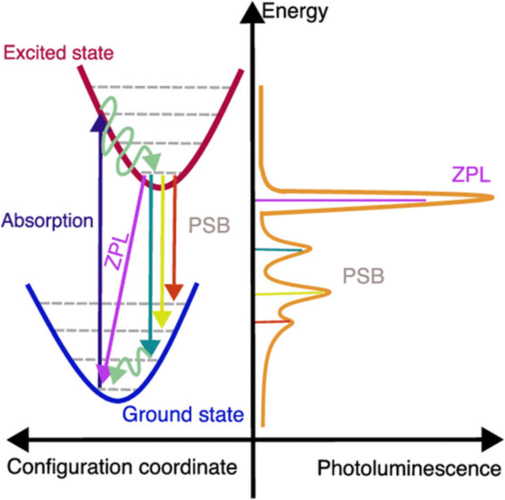
Left: Configuration diagram of ground and excited electronic states, each with several vibrational levels indicated by dashed lines. Transitions are illustrated by straight lines (optical) or wavy lines (vibrational). Right: The corresponding PL spectrum of this vibronic transition showing a ZPL and accompanying phonon sideband (labelled PSB). Reproduced with permission from Cholsuk et al.. 51 © 2023 American Chemical Society.
The arrangement of atomic nuclei will be different in the ground and excited electronic states due to the electron orbitals differing in their spatial distributions. The Franck–Condon principle states that electronic transitions occur on timescales much faster than the relaxation of nuclei.
52
Thus, if the ground and excited states have a larger difference in their nuclear configurations, it will be more likely for electrons to be excited into higher vibrational modes, where the lattice is distorted to a greater degree. The mechanism for these so-called vibronic (vibrational + electronic) transitions was first described quantitatively by Huang and Rhys in 1950.
53
The coupling of vibronic transitions can be calculated from the difference between the equilibrium lattice configurations in the ground and excited states which can, in turn, be modelled using density functional theory (DFT).
54
The Huang–Rhys factor
Reported figures-of-merit for single-photon emitters in h-BN and other material platforms. The best-performing platforms for each metric are indicated in

SC: semiconductor; RT: room temperature.
*Defect structure proposed but not conclusively confirmed.
Estimated from PL spectrum in Gao et al. 50
Background subtraction has been applied.
Resonant excitation scheme used.
h-BN defects as single-photon emitters
Applications such as simple quantum key distribution (QKD) protocols and quantum random number generation (QRNG) require single-photon sources with a high purity – that is, a high probability of exactly one photon being emitted. Other applications, such as all-optical quantum computing 67 and repeaters in quantum networks,68,69 go further and require that these photons be indistinguishable from one another. Despite requiring cryogenic operating temperatures, current leading platforms include epitaxial III–V quantum dots (these offer high-purity sources with a high degree of spectral tunability)66,70,71 and negatively charged silicon–vacancy (SiV−) centres in diamond (these have excellent spectral stability with emission that can be down-converted to telecom wavelengths).24,72 Since their discovery in 2016, colour centres in h-BN have emerged as an alternative solid-state single-photon source.37,73
The purity of a single-photon source can be measured by performing Hanbury Brown and Twiss (HBT) interferometry.
74
This involves passing the emitted light through a 50:50 beam splitter and sending the two streams of photons to separate detectors, where coincidence events at time difference 
Since
For a coherent photon source, the spectral linewidth of the emission is ideally lifetime limited. For many room-temperature defects in h-BN, the ZPL is much broader than this; this is generally attributed to spectral wandering during the acquisition time of the spectrum. Further research into the temperature dependence of the ZPL and the timescales of spectral wandering are required in order to fully understand this. To measure the indistinguishability of photons, a Hong–Ou–Mandel (HOM) experiment can be performed.
79
This is a two-photon interference experiment where two streams of photons are sent to different input ports of a 50:50 beam splitter. For indistinguishable photons, destructive interference of their wavefunctions results in both photons exiting the beam splitter from the same output port; again, a dip in coincidence events is therefore observed. The degree of indistinguishability is described by the visibility of the dip and varies from
HBT autocorrelation and HOM cross-correlation tests are commonly employed across the literature to measure the quality of single-photon sources. A recent study by Fournier et al. measured the so-called B-centre (a particular blue-emitting defect in h-BN) as emitting single photons with
Another factor to consider is the source brightness as this limits the rate at which photons can be generated and therefore the usefulness of a source for different applications. There are several ways of quantifying the brightness of a single-photon source:
80
one benchmark is the saturation intensity
With a high brightness and quantum efficiency, 82 colour centres in h-BN look to be a promising platform for quantum photonic technologies. This has been affirmed with proof-of-concept demonstrations of QKD83,84 and QRNG,85,86 as well as a single-qubit photonic processor using an h-BN defect as the single-photon source. 87 However, in the near future it is likely that III–V quantum dots, with their superior purity and indistinguishability, will remain the platform-of-choice for some of the purely optical applications. For a recent, comprehensive review of h-BN defects’ performance in QKD and QRNG, the reader is referred to Çakan et al.. 88 Additional opportunities for h-BN defects lie with the spin-active colour centres, where optically controllable spin states could allow scalable, room-temperature spin–photon interfaces in a 2D system to be developed. Properties and applications of these spin defects are explored in the following section.
Spin properties
Spin Hamiltonian
For a defect to be used as a qubit, it needs a spin state which can be controlled and read out with high fidelity, ideally at room temperature. Like the NV− in diamond, many promising defects in h-BN have spin-triplet ground states;30,89 as explained later, this is often advantageous. The Hamiltonian for a spin 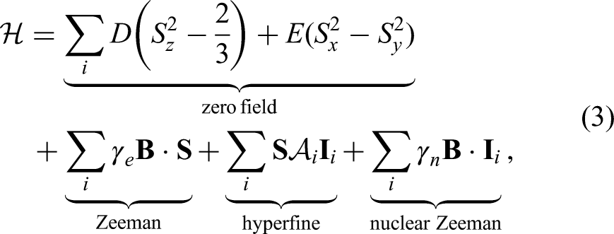
External fields perturbing the Hamiltonian allow for the sensing of said fields by measuring the subsequent change in energy levels. This forms the basic principle behind using spin defects as sensors.89,90 Due to the 2D nature of h-BN, spin defects can be situated extremely close to a sample being measured. Combined with the atomic size of point defects, this allows for extremely high spatial resolution. Magnetometry – either using single defects
91
or VB− ensembles
89
– is the most well-studied sensing application. The defect studied by Gilardoni et al. (an unknown carbon complex with
Decoherence of h-BN defects
Coherent control of a qubit is the ability to manipulate its quantum state whilst preserving knowledge of its phase. This losing of phase information is called decoherence and occurs from unknown interactions with the environment. Any interaction which changes the energy splitting between computational states
The coherence time (
Comparison of reported spin coherence times of defects in h-BN with other solid-state spin qubit platforms. Measurements were performed at the temperature indicated and in magnetic fields below 1T unless otherwise stated. The best-performing platforms for each metric are indicated in

SC: semiconductor; RT: room temperature.
*Defect structure proposed but not conclusively confirmed.
Nuclear spin control is demonstrated by Bourassa et al. but the coherence time is not measured. 104
At high magnetic fields (
More advanced pulsed sequences can be implemented to repeatedly refocus a dephasing spin. This could in principle continue indefinitely. However, imperfect pulse sequences also contribute to decoherence by introducing ‘gate-induced’ errors. These pulse sequences are called dynamical decoupling sequences as they act to extend coherence times by decoupling the electron from its spin environment. The term
Mechanisms that couple between
Electronic spin control
So far, the control of spin states has been treated in the abstract, without consideration for how the spins are actually manipulated in a laboratory. In this section, the experimental protocol for achieving coherent control of defects’ electronic spins is outlined. This discussion is then extended to nuclear spin control in the next section.
The first step in spin control is to initialise into a particular spin state. A useful feature of many
Spin resonance experiments can be used to probe
Optically detected magnetic resonance (ODMR) is a related technique which takes advantage of spin-dependent relaxation pathways in spin defects to read the spin state directly from the PL intensity.
118
During this process, a laser is used to initialise the spin state and the fluorescence from the defects is monitored. When resonant transitions occur, and the spin state is changed, the PL intensity will increase or decrease accordingly. The optical readout allows ODMR to be implemented within confocal microscopes so that individual defects can be studied in addition to defect ensembles; ODMR has therefore emerged as the standard technique to investigate optically active spin defects in solids.48,118 Contrary to conventional EPR, ODMR experiments typically keep the

ODMR spectra of VB− ensembles at 8.7 mT in isotopically purified h-BN (top) and h-BN with a natural isotopic abundance (bottom). Solid lines depict multi-peak Lorentzian fits and the shaded regions show simulated ODMR spectra. Adapted from Gong et al. 119 under a CC BY 4.0 licence.
Figure 3 shows how the frequencies of the VB− spin resonance transitions evolve as the 

Tracking the spin resonance frequency of VB− ensembles as a function of magnetic field. Experimental data are indicated by diamonds and theoretical models plotted as solid lines. (a) ODMR measurements at 5 K and 295 K. At zero-field, the transitions occur at microwave frequencies of
Whilst cw ODMR allows for the initialising and readout of
Nuclear spin control
Nuclear spins in the proximity of a defect can be used to store coherent quantum information for longer periods of time. Multi-qubit nodes comprising nuclear spins controlled via a single defect's electronic spin have been realised in diamond101,123–126 and SiC 104 To control the nuclear spins via the electron spins, a series of controlled-NOT (CNOT) gates is used to swap the electronic and nuclear spin states. Generally, this is based on electron–nuclear double resonance (ENDOR) pulse sequences21,45 but more complex gates have also been demonstrated. 126
Specific implementations of the swapping procedure depend on the nature of the electronic structure and hyperfine coupling of a particular defect but a simple example for an
In h-BN, coherent control of nuclei had until recently only been achieved using VB− ensembles coupled to the three nitrogen nuclei neighbouring each defect.
45
Single-defect studies had been limited by only finding weak hyperfine signatures believed to arise from nitrogen nuclear coupling,
30
or by not observing any hyperfine signatures at all.
49
Gao et al. recently reported control of individual 13C nuclei using a single defect.
50
This study used an ENDOR sequence similar to the approach outlined above, with nuclear spin states read out by mapping them back onto the electronic spin. This was made possible by the defect's strong hyperfine coupling (300 MHz). In this study, they perform nuclear Rabi oscillations with Rabi frequencies approaching 1 MHz and a
The abundance of nonzero nuclear spins in h-BN means that it will not be possible to detect or control distant nuclei as has been achieved in diamond.127,128 However, the recent results by Gao et al. have demonstrated that nuclear spins intrinsic to the defect still present an opportunity for controlling and storing information on individual nuclei. This resulted in the longest coherence time of a defect in h-BN to date of 162 μs (see Table 2). This is believed to be limited by the electronic
Defect engineering
Identifying defects
In order to produce scalable photonic devices using colour centres, one must be able to deterministically create the defect of interest. A key step towards this is understanding the atomic structure of the defect itself. However, assigning structures to observed defects is not a trivial feat. The identification process consists of comparing the predictions of theoretical models to experimental observations,51,129 as well as calculating the formation energies of defects and their charge state stability.
130
DFT modelling of a defect's electronic structure can be used to predict the ZPL energy and the polarisation characteristics of optical transitions.131,132 The phonon density of states can also be calculated and weighted by
Experimentally, cryogenic cooling of samples increases the resolution of the sideband structure, and photoluminescence excitation (PLE) spectroscopy can be used to probe the sideband structure in absorption spectra. 133 However, an outstanding challenge in the field is that different defect structures are predicted to have similar PL spectra. 134 Because of this, it may prove impossible to unambiguously assign defects in h-BN from PL spectra alone. It can also be unclear whether variations in ZPL energies between defects arise from different structures, local variations in strain environment, or a combination of both.
It is easier to positively identify spin-active defects since the measured spin Hamiltonian parameters provide additional comparisons to theory.43,135 This was the case with the VB−, which displays a spin-triplet ground state with zero-field splitting and hyperfine coupling consistent with atomistic modelling. 43 The isotopic dependence of the hyperfine signature136,137 and the observation of excited-state ODMR 138 have since confirmed the VB− structure beyond doubt. Many individually addressable spin defects in h-BN have been attributed to various carbon complexes30,47–50. A summary of potential structures can be found in Table 3. The role of carbon doping in the formation and stability of colour centres in h-BN has long been studied, 116 and in recent years theoretical models for different carbon-based defects have been developed to attempt to unveil the structures responsible for quantum emission from h-BN. Many candidates have been proposed including single substitutionals (CB and CN),134,135 dimers (either C2 or separated CB–CN donor–acceptor pairs),134,135 trimers,133,135,139 tetramers,140,141 and C6 rings, 142 as well as additional complexes containing antisites, vacancies, and oxygen substitutionals.130,143 Of these, the CNCB3+ symmetric tetramer has been suggested as being the origin of the defect studied by Guo et al., 49 and CBON+ seems a strong candidate for one of the defect classes studied by Gao et al. 50 From the data presented in Table 3, it is clear that the evidence for the CBON+ structure is substantially stronger than that of CNCB3+.
Evidence for structures proposed to explain spin defects in h-BN. Theoretically predicted values are indicated by ‘th.’ and experimentally measured values by ‘exp.’

At the ensemble level,
An additional tool which has been proposed to aid in defect identification is electron microscopy. Annular dark-field (ADF) imaging can be used to directly visualise point defect structures in very thin h-BN samples. 145 The challenge here arises in correlating these findings with optical emission since the resolutions of optical and electron microscopy are vastly different, and many defects will exist within the confocal volume, despite only one being responsible for the emission.146,147 A recent study by Liang et al. was able to identify a blue-emitting colour centre as originating from boron intercalant atoms. 148 Here, high-angle ADF imaging of the h-BN sample was used to shortlist potential defect structures. These structures were then modelled using DFT to determine which was the likely source of the observed emission. This is an innovative approach capable of providing direct evidence for particular defect structures.
Creating defects
There exist many techniques to introduce defects into crystals. These include ion implantation to incorporate a specific atom species into the lattice, irradiation to generate vacancy–interstitial ‘Frenkel’ pairs, and thermal annealing to mobilise defects so that larger complexes can form. 149 An ideal defect creation process would be capable of fabricating a single defect on demand with full control of its position, whilst avoiding the creation of undesired defects nearby (particularly paramagnetic defects contributing spin noise). As with most areas in spin defect research, the most progress made in this regard is with the NV− centre in diamond. It is well understood that this defect can be produced in nitrogen-containing diamond with two steps: first, irradiating to generate vacancies; second, annealing to mobilise these vacancies until they latch on to a nitrogen impurity atom. 149 The most successful technique to progress this from a bulk process to one with position-specific formation is defect laser writing. 150 This approach uses pulsed lasers to generate vacancies and provide localised annealing. Improvements to this technique have allowed for the production of arrays of single NV− centres with near-unity yield and sub-micron positional precision. 77 This method has also been extended to other defects in diamond. 151
In h-BN, VB− ensembles can be readily generated through a variety of irradiation techniques including using electrons, 152 neutrons, 42 and focused ion beams.153,154 There have also been several reports of site-selective generation of single defects; although, as yet none of these have produced spin-active defects. As shown in Figure 4, B-centres have been reproducibly created using electron beam irradiation.57,155 Other single defects in h-BN have been created by irradiating samples with electron beams 156 and helium ions, 148 and by using femtosecond laser writing.157–159 To transfer this site selectivity to a particular spin-active defect, it would be useful to first know the atomic structure of the defect. As explained at the beginning of this section, this has proven difficult to ascertain and there is much active research trying to identify defects of interest. Until now, the creation of spin-active defects in h-BN has been limited to the non-deterministic approach of carbon doping the entire sample, resulting in a low yield of the desired defect.50,129

Deterministic creation of B-centres in h-BN using a 15 keV electron beam with a 33 nm spot size. (a) PL map of irradiated sites showing localized emission from eight regions. With 1000 s of irradiation, ∼ 20 individual defects were formed at each site. (b) Low temperature PL spectra of the emission from these eight sites each showing a reproducible ZPL at 436 nm. Reproduced from Fournier et al. 57 under a CC BY 4.0 licence.
Another important factor to consider with h-BN defects is the growth process of the material itself. Since this controls the initial state of the crystal, including which defects are already present in the lattice, it is sensible to consider this alongside the defect creation process. Bulk single crystals of pristine h-BN can be produced by high-temperature high-pressure methods 160 or chemical vapour deposition (CVD). Exfoliated flakes of high-purity crystals can then be used as the starting point for the defect creation processes listed above. Single h-BN crystals can also be grown at atmospheric pressure from a flux, most notably by using a Ni–Cr solvent.161,162 An alternative approach is to use epitaxial growth methods such as metal–organic vapour-phase epitaxy (MOVPE) 163 or molecular-beam epitaxy (MBE) 164 to produce wafers of h-BN. With many of these techniques, impurities such as carbon can be controllably incorporated into the lattice during growth. In the case of MOVPE, an organoborane precursor such as triethylborane (TEB) acts as the carbon source. The concentration of carbon defects can then be controlled by adjusting the TEB flow rate. 129 For MBE, there are a variety of carbon sources that can be utilised to introduce carbon into the lattice.129,165 For CVD-grown h-BN, a recent study was able to directly engineer carbon-defect formation by altering the growth conditions. 166
The isotopic composition of the crystal is a further consideration to be had. This can be controlled when growing crystals via the flux method.167,168 As shown in Figure 2, purifying the isotopes of boron and nitrogen (and thus homogenising their nuclear spins) leads to a better-resolved hyperfine structure in the VB− ODMR spectrum.
119
Gong et al. found that
Device integration
For solid-state quantum technologies to be scalable, they need to be integrated into on-chip devices.
13
A major hurdle to the scalability of diamond-based systems is one of efficiently incorporating defects into photonic chips without compromising the quality of the defects. This should be more straightforward with a layered host material which is more conducive to integration with photonic circuits.34,35 The fabrication of monolithic nanophotonic components has been demonstrated using h-BN; these include optical cavities with quality factors exceeding 3000
169
and resonators with quality factors exceeding 4000.
170
Moreover, emitters in h-BN have been integrated with non-monolithic structures including single-photon coupling to AlN waveguides with
Additionally, van der Waals heterostructures can be assembled to alter the properties of the host material. For example, graphene electrodes have been used to control defect charge states by altering the Fermi level. 175 This may be able to prevent defect charge-state switching which is observed for several species of single defect.30,50 Electrodes can also be used to tune the emission from h-BN defects by exploiting the Stark effect; ZPL shifts of up to 43 meV have been recorded.176,177 ZPL shifts of up to 65 meV have also be achieved by applying strain.41,178 The versatility of 2D materials means that there are a variety of methods that can be used to apply electric or strain fields; Yu et al. provide a recent review of these techniques. 179 Studies have shown that emission from different defects in the same sample respond differently to applied strain; this could be due to local strain variations before any external strain is applied and may explain the variations in ZPL energies observed, even for the same defect species.178,180 The ability to control the wavelength of emission is vital in eliminating spectral inhomogeneities between different defects and would improve compatibility between h-BN defects and other platforms in potential hybrid quantum technologies.
Conclusions & outlook
Spin-active colour centres in h-BN provide a promising route towards scalable quantum technologies and justify the recent attention they have gained. They allow for room-temperature control of individual electronic and nuclear spins using simple optical and spin resonance techniques, and are compatible with on-chip nanophotonics.
Research into h-BN defects is a rapidly moving field which is benefitting from the wealth of existing research into both 2D materials and spin defects in other host materials. A review of quantum photonics using 2D materials by Turunen et al. from 2022 outlined several key milestones which need to be met. 35 Some of these have already been achieved such as demonstrations of photon indistinguishability and individual nuclear control; others, such as demonstrating spin–photon entanglement, remain outstanding. Several principles including photon indistinguishability, emission tunability, and site-specific defect creation have been demonstrated for colour centres which are not spin active. Whilst this is sufficient for developing coherent single-photon sources, for applications requiring a spin–photon interface, this needs to be replicated for spin-active defects too.
The first application to be realised for the spin-active h-BN defects will likely be room-temperature high-resolution scanning magnetometry. This is due to the layered nature of h-BN allowing for defects to be in very close proximity to the surface. The current leading platform for such magnetometry is the NV− centre, but the carbon complex used by Gilardoni et al. has a major advantage in that it can perform vector magnetometry using a single defect. 91 The sensitivity of such schemes can be improved by prolonging the spin coherence of the system, with further work on dynamical decoupling and nuclear spins providing possible avenues towards this. If coherence times can be extended into the millisecond range, and spin–photon entanglement is demonstrated, it then becomes more feasible that these defects can also be used as a short-term quantum memory for deployment in quantum networks.
Footnotes
Acknowledgments
I would like to thank Hannah Stern for her valuable support and suggestions during the preparation of this literature review.
Author contribution(s)
Funding
The author's doctoral studies are supported by the Royal Society and Trinity College, University of Oxford.
Declaration of conflicting interests
The author declared no potential conflicts of interest with respect to the research, authorship, and/or publication of this article.