
Abstract
A voltage mode capacitance multiplier for ultra-low frequency physiological signal processing is designed with a circuit model. With the proposed multiplier, a filter can achieve a cutoff frequency of 12 mHz with a 1 pF basic capacitance and a 10 kΩ resistor. The corresponding multiplication factor will be 1.35 × 10⁹. By changing the controlling terminal, the multiplication factor can be widely tuned from 1950 to 1.35 × 10⁹ and the corresponding filter cutoff frequency will be from 12 mHz to 8.15 kHz. According to the circuit model, to further increase the multiplication factor to decrease the chip area, more multiplication stages can be added to the feedback loop.
Introduction
Integrated circuits are potential building blocks in miniature medical instrumentations such as portable, wearable, and implantable devices.1–8 Physiological signal processing after obtaining from sensors is an important part of the whole system. Most physiological signals are in the range of near direct current (DC) to 10 kHz. As a result, ultra-low frequency filters will be needed, which usually means large capacitance, large resistance, and small transconductance amplifier. Large resistance or capacitance will occupy a large chip area, which means a large system volume and high cost. It is not feasible for on-chip implementation. Besides, the values of passive components are sensitive to process conditions. As a result, circuits can be designed to be equivalent to the large passive component. Many groups have started to research in these fields. To get large grounded capacitance, current mode,9–13 voltage mode,14–16 active elements based,17–27 and non-balance capacitance multipliers 28 have been designed. However, there are also some problems to be solved. Firstly, the tunable range should be increased to make the circuit suitable for more physiological signal processing. Secondly, the design method should be more transplantable. It should not be just for only one application. Thirdly, in the traditional current mode multiplier, there is a trade-off between increasing multiplication and decreasing power consumption, which should be improved.
In this paper, a voltage mode multiplier is designed based on a simple circuit model. By using a metal–oxide–semiconductor field-effect transistor level circuit to realize the component in the model, we obtained a very flexible and transplantable design method. A widely tunable range of multiplication can be achieved. More gain stages can be added in the feedback loop to further increase the multiplications to decrease the chip area.
Circuit design
A simple model of voltage mode capacitance multiplier can be shown in Figure 1. We can get the equivalent capacitance from this model


A simple model of voltage mode capacitance multiplier.
K + 1 is the multiplication factor and K is the total gain of the multiplication stages. The multiplication stages will be amplifiers. To get the equivalent capacitance in equation (1), the output signal must have the opposite direction with the input signal. The gain-controlling part will tune the multiplication factor by an external voltage. The structures and number of the amplification stages can be chosen according to specific applications based on this model.
In this paper, the specific circuit structure of the voltage mode capacitance multiplier will be decided in order to get widely tunable multiplication, which can be seen in Figure 2. There are three stages in the feedback loop, the first stage is a buffer, the second stage is a T-type inverting proportional amplifier to ensure a high gain as well as the opposite direction of input and output, and the third stage is a positive proportional amplifier. MA, MB, and MC are used as resistances. The equivalent capacitance can be expressed


The structure of the proposed capacitance multiplier.
By setting, (RA + RB)/R1, (RA//RB)/R2, and RC/R3 as large values, a high multiplication factor can be achieved. RC is the equivalent resistance of MC, RB is the equivalent resistance of MB, and RA is the resistance of MA. By changing the gate voltage of MA, MB, and MC, the resistance can be changed, and the equivalent capacitance and the multiplication factor will be widely tuned.
To ensure the equivalent capacitance in equation (2), the operational amplifier (OPA) in Figure 2 should have a high gain. For the traditional two-stage amplifier, the bandwidth will be too narrow for physiological signals with a range of nearly DC to 10 kHz when the gain is as high as 90 dB. Because for a specific structure, there will be a trade-off between bandwidth and gain. As a result, a three-stage amplifier is adopted in this paper as shown in Figure 3.

The structure of the operational amplifier (OPA).
Based on the circuit model in Figure 1, more gain stages can be added in the feedback loop to further increase the multiplications to decrease the chip area. As a result, a transplantable and flexible design method of capacitance multiplier based on a circuit model is found.
Simulation results
The proposed capacitance multiplier is designed in 0.18 μm complementary metal–oxide–semiconductor (CMOS) technology with a supply voltage of 1.8 V. The dimensions of the components in the proposed circuit are shown in Table 1.
The dimensions of the devices in the proposed capacitance multiplier.
The layout of the circuit is shown in Figure 4. The area of the layout is about 116 μm × 71 μm. The parasitic parameter has been extracted from the layout. Both pre- and post-layout simulations are done with the circuit.

The layout of the proposed capacitance multiplier.
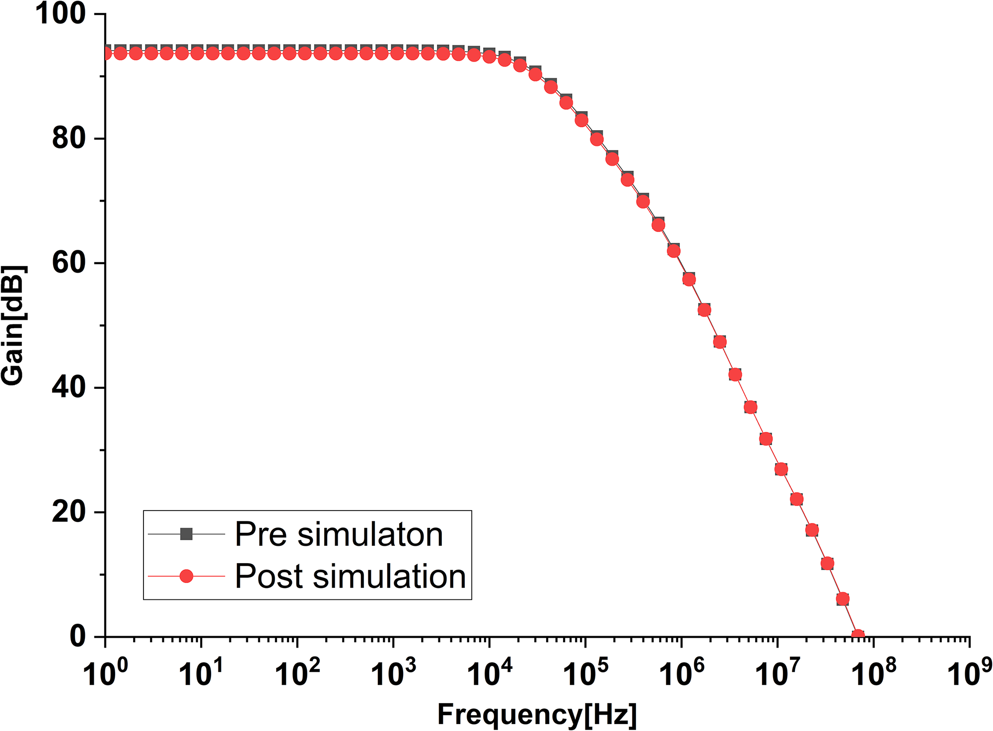
The gain and bandwidth of the OPA are about 94 dB and 43 MHz as shown in Figure 5. The pre- and post-simulation have nearly the same result. According to the simulation result, we can see that the gain of the amplifier is large enough to be used as an ideal OPA, and the bandwidth of the amplifier is wide enough to process physiological signals.
The frequency characteristics of the operational amplifier (OPA).
To verify the performance of the proposed circuit, the multiplier is connected with a resistor to form a simple first-order low-pass RC filter. As shown in Figure 6, the cutoff frequency of the filter changes from 12 mHz to 8.15 kHz when tuning VC. The pre- and post-simulation curves are nearly coincident.

The alternative current (AC) analysis of the filter output when tuning VC.
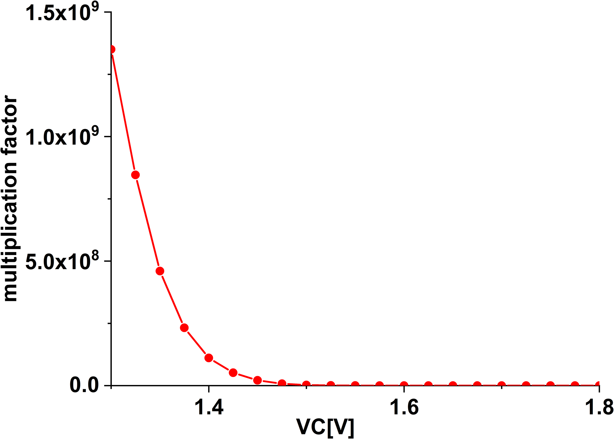
The multiplication factor of the multiplier varies from 1950 to 1.35 × 10⁹ when tuning VC as shown in Figure 7. The highest multiplication factor is obtained when VC = 1.3 V.
The multiplication factor under different control voltage VC.
The transient simulation result of the filter output with a sine wave of different amplitude at 1 mHz as an input signal is shown in Figure 8.

Transient analysis of the low-pass filter.
Corner analysis of the frequency characteristics of the RC filter when VC = 1.3 V is shown in Figure 9. The cutoff frequencies under tt, ff, ss, snfp, and fnsp are 12 mHz, 1260 mHz, 179 mHz, 140 mHz, and 228 mHz. The simulation results are shown in Figures 7–9 all come from post-layout simulation.

The corner analysis of the frequency characteristics of the low-pass filter.
The proposed circuit will be used in a low-frequency field, so the post-layout simulation results are expected to be very close to the actual situation. The terminal VC can be tuned to find a suitable multiplication factor in actual testing after tape-out in the future.
A summary of performance comparison with other works is shown in Table 2. The maximum multiplication factor and the tuning range of this work are excellent. However, the power consumption of this work is average. Because the bandwidth of the OPA should be large enough to cover most kinds of physiological signals. There is a trade-off between bandwidth and power consumption under a certain OPA structure. A more optimized OPA structure should be developed to decrease the power consumption in the future.
Summary of performance comparison.

CMOS: complementary metal–oxide–semiconductor.
Conclusion
A capacitance multiplier design method based on a model is proposed in this paper. By using a three-stage structure in the feedback loop, the multiplication factor can be as high as 1.35 × 10⁹. When tuning the external voltage VC, the multiplication factor of the multiplier varies widely from 1950 to 1.35 × 10⁹. To further increase the multiplication factor to decrease the chip area, more multiplication stages can be added to the feedback loop. As a result, a transplantable and flexible design method of capacitance multiplier based on a circuit model can be found in this paper. The proposed circuit can be used in the low-frequency field. Besides, the proposed structure can also be used in the circuit which needs a large on-chip passive component. The chip area and the system volume can be largely reduced by using the proposed method.
Footnotes
Author contribution
Li Yan carried out the concepts, performed the design and simulation work, and finished the manuscript writing.
Declaration of conflicting interests
The author declared no potential conflicts of interest with respect to the research, authorship, and/or publication of this article.
Funding
The author(s) disclosed receipt of the following financial support for the research, authorship, and/or publication of this article: This work was supported by Education Reform Project of Beijing Information Science and Technology University (Grant No. 2020JGYB41), National Natural Science Foundation of China (Grant No. 62101054), Foundation of the state key laboratory of Transducer Technology (Grant No. SKT2201), R&D Program of Beijing Municipal Education Commission (Grant No. KM202211232005).