
Abstract
Modular multilevel converters are widely used voltage source converters in a variety of applications, such as power transmission, renewable energy, and motor drives. Nevertheless, they introduce complexity to control methods and data processing, hence requiring additional sensors. Pulse width modulation and voltage balancing algorithms are essential for modular multilevel converters, and there are several approaches available to achieve voltage balance. This study presents a revised approach to multicarrier pulse width modulation for the modular multilevel converter, which incorporates a combination of DC carriers. This modulation approach employs the interleaving of the modulated waveform with a direct current (DC) level, while ensuring the preservation of quarter wave symmetry. This method has led to a reduction in the switching frequency of the Modular Multilevel Converter (MMC). Moreover, the paper covers the implementation of op-amp based capacitor measuring and sorting circuits for capacitor voltage balancing in a modular multilevel inverter with R load. Using a combination of direct current (DC) and triangular carriers in the PWM, the proposed method demonstrates a reduction in THD from 27.55% to 21.76% in phase voltage and switching frequency by 20%. The effectiveness of the method has been confirmed using Simulink/MATLAB. The simulation and experimental findings reveal a notable reduction as compared to conventional multicarrier PWM technique for modular multilevel converter (MMC) and find that the unique approach performs superiorly without compromising the integrity of the output voltage.
Keywords
Introduction
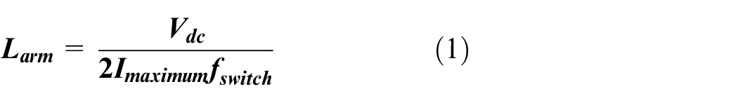
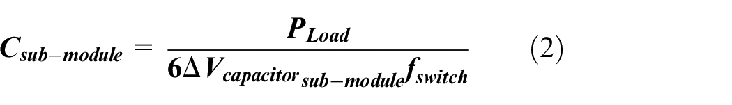
The current trend in power generation suggests a growing prominence of distributed generation utilizing nonconventional energy sources. Additionally, there is a preference for long-distance and international transmission of high power using HVDC transmission. Moreover, converters are being increasingly implemented with a multi-level configuration, as opposed to a two-level configuration. 1 The utilization of modular multilevel topology (MMC) has been found to be effective in attaining a high-quality output voltage. 1 The MMC system consists of two arms that are interconnected by two buffer inductors per phase. Every arm consists of several power switches that are interconnected in series to a dc-link. The MMC, or Modular Multilevel Converter, serves as a crucial component in high-voltage direct current (HVDC) power transmission systems. It finds application in the integration of offshore wind power systems beneath the sea and the establishment of long-distance on-shore connections. 2 The MMC power converter exhibits favorable characteristics such as high output quality, efficiency, significant scalability, modularity, and a high degree of redundancy and fault tolerance. 3 The implementation of Modular Multilevel Converters (MMC) presents various technical challenges. 4 These challenges include determining the optimal size of the arm inductor 5 and sub-module capacitor 6 to ensure cost effectiveness and compactness. Additionally, the selection of the appropriate type and rating of the submodule is crucial. 7 Pre-charging the floating sub-module capacitors to their nominal voltage is necessary, as is regulating the voltage of the sub-module capacitors at the reference voltage level to generate a multilevel stepped wave. Accurate measurement of the sub-module capacitor voltages is essential, as is the suppression of voltage ripples 8 at the sub-module capacitor. Furthermore, it is important to suppress negative sequence circulating current, 9 incorporate fault-tolerant operation features, achieve an equal distribution of switching action among sub-modules, and minimize the switching operation of the sub-modules. 10
(a)
Where,
(b)
where
(c)

Here, R is the pre-charging resistor.
(d)

Where, N is the number of sub-modules.
Researchers have made significant contributions toward addressing the aforementioned issues in order to enhance the performance of MMC. 11 Firstly, the complex structure of the system arises due to the necessity of effectively managing firing signals. Secondly, frequent sampling of voltage and current sensors leads to a substantial interchange of data. Lastly, the balancing of a floating capacitor is a critical requirement in the system. 12 Typically, multi-module configurations (MMCs) consist of two arms inside a phase, each containing identical submodules. Modified Modular Multilevel Converter (MMC) can be implemented in several ways. 13 One approach involves using a single arm with a decreased number of modules, resulting in reduced switching. 14 Another approach involves using interconnected submodules within the arm. Alternatively, multiple types of sub-modules can be used within a single arm, or additional devices can be placed alongside the submodules. Certain factors contribute to an increase in switching behavior. However, the determination of the weighting factor in this method is a complicated task. 15 The process of achieving equilibrium in arm capacitor voltages can be accomplished through the utilization of two distinct methodologies. The initial approach assumes that the capacitances of the various capacitors in the arm are equal, and voltage balancing is implemented. An alternative perspective posits that the capacitances of the various capacitors inside the arm exhibit variability, and an energy balancing technique is employed. 16 The voltage balancing technique involves the measurement and sorting of the voltages of arm capacitors in a straightforward manner. 17 The sub-modules with the highest or lowest capacitor voltages are placed based on the direction of arm current. Nevertheless, while implementing this balancing technique throughout each cycle, it is evident that the total on state sub-modules of the arm remain unaltered, yet there is still an occurrence of unneeded switching. In order to address this issue, a voltage balancing method known as reduced switching frequency (RSF) was devised. 18 The Modular Multilevel Converter (MMC) uses a strategy to maintain a consistent DC side voltage for each phase by introducing N sub-modules out of 2N at any one time. The placement of N-non sub-modules is recommended in the upper arm, while non sub-modules should be in the lower arm. To ensure a consistent and equitable distribution of voltage across capacitors, capacitor voltage balancing techniques are employed. The arm current effect is used to determine the number of sub-modules to be inserted during the current sample period. The voltage sub-modules, N-on, are implemented when the arm current is positive, while N-non sub-modules are used when the arm current is negative. The number of sub-modules introduced or bypassed depends on the specific requirements of the application. Carrier phase shifted pulse width modulation (CPSPWM) has conventionally been regarded as the pulse width modulation (PWM) approach that exhibits the largest number of device switching instances. 19 Several strategies have been employed to mitigate power device switching in the context of powerelectronics. 20 These strategies include the modification of carrier phase shifted pulse width modulation (CPSPWM), employment of nearest level modulation (NLM), 21 utilization of space vector modulation (SVM), 22 and implementation of level shift pulse width modulation (PWM). 23 In high voltage applications, the NLM 24 method can improve harmonic performance by increasing output phase voltage levels to 2N + 1. However, when used in medium applications with a small number of SMs, the output voltage contains low order harmonics, causing high total harmonic distortion (THD) of output current. The Selective Harmonic Pulse Width Modulation (SHEPWM) 25 method achieves better harmonic performance with low switching losses but increases computational burden with large amounts of SMs. The Space Vector PWM 26 method provides flexibility in choosing voltage vectors to acquire multiple objectives but increases computational burden exponentially with increasing SMs. Multi-Carrier Pulse Width Modulation (LS-PWM) is divided into Level Shifted Pulse Width Modulation (LS-PWM), Phase Disposition Pulse width modulation, Phase Opposition Disposition Pulse Width Modulation (PODPWM), and Alternative Phase Opposition Disposition Pulse Width Modulation (APODPWM). PDPWM uses the same phase for upper and lower triangular waves, PODPWM uses the same frequency and amplitudes, and APODPWM uses a 180° phase shift. 27 The PDPWM method for the MMC has better harmonic performance than the phase shifted carrier pulse width modulation (PSCPWM) method, but requires hundreds of carriers. The improved PDPWM method for the MMC is easy to implement and only needs a single or double carriers. To improve the harmonic performance of the NLM method for the hybrid MMC,28,29 the authors proposed the nearest level PWM (NL-PWM) method for the hybrid MMC, which distributes PWM signals evenly between HBSMs and FBSMs. However, the traditional PDPWM method for the MMC is relatively complex and difficult to implement due to the number of carriers needed.
Research gap
Although Modular Multilevel Converters (MMC) have made significant improvements, there are still unaddressed research gaps, particularly in the fields of efficiency, control complexity, and scalability.
Analysis of control system complexity
Contemporary MMC systems generally utilize intricate control algorithms the need substantial technology, particularly for the purpose of capacitor voltage balance and modulation approaches. Notwithstanding the introduction of modulation methods like CPSPWM and NLM, the complex structure of real-time control and the computational load for high-level converters remain significant obstacles. There exists a necessity for the development of control techniques that are more compact and capable of preserving performance while minimizing computational burden and enhancing rapid adaptability.
Analysis of switching losses and system efficiency
While much research has been conducted on minimizing switching losses using novel modulation approaches, such as lower switching frequency methods, there is a scarcity of studies on scalable solutions that effectively optimize both switching and conduction losses for high-voltage, high-power applications. A additional topic that requires further investigation is the trade-off between Total Harmonic Distortion (THD) and switching frequency in traditional approaches.
Scalability to higher-level converters
While most current research concentrate on five- or nine-level Multilevel Converters (MMCs), there is a lack of thorough investigation on the scalability of suggested modulation and control methods to converters with more than 15 levels. The present research does not sufficiently address the added complexity introduced by high-level converters in terms of switching control, voltage balancing, and thermal management.
Thermal control and dependability
Increased switching frequencies in modular multilevel converters (MMCs) can result in substantial thermal strains on power electronics components. Although some studies have concentrated on thermal performance, there is a dearth of extensive study on efficient thermal management strategies in MMCs, especially for applications that need uninterrupted high-power operation. Further work is necessary to assess the reliability during long-term heat cycling.
Techniques for balancing capacitors
Contemporary methods for balancing capacitor voltage, such as sorting algorithms, are frequently constrained by the intricacy of hardware and the limitations of sensors. Despite the proposal of estimation-based approaches to reduce hardware requirements, these strategies may nonetheless contain inaccuracies that negatively impact system performance. Further study is required to optimize capacitor balancing methods that minimize hardware complexity while maintaining precision.
Renewable energy systems integration
Given the rising significance of including renewable energy sources into power grids, Multi-Modal Converters (MMCs) are being utilized more and more in High Voltage Direct Current (HVDC) transmission systems for offshore wind farms and other similar renewable energy applications. Nevertheless, current studies fail to adequately tackle the particular obstacles for combining MMCs with variable renewable energy sources, such as sporadic power provision and voltage variations.
An essential challenge in current Modular Multilevel Converter (MMC) systems is the compromise between the frequency at which switching occurs, the efficacy of harmonics, and the complexity of control. Traditionally used modulation methods, although successful in decreasing total harmonic distortion (THD), sometimes encounter significant switching losses and higher computational demands.
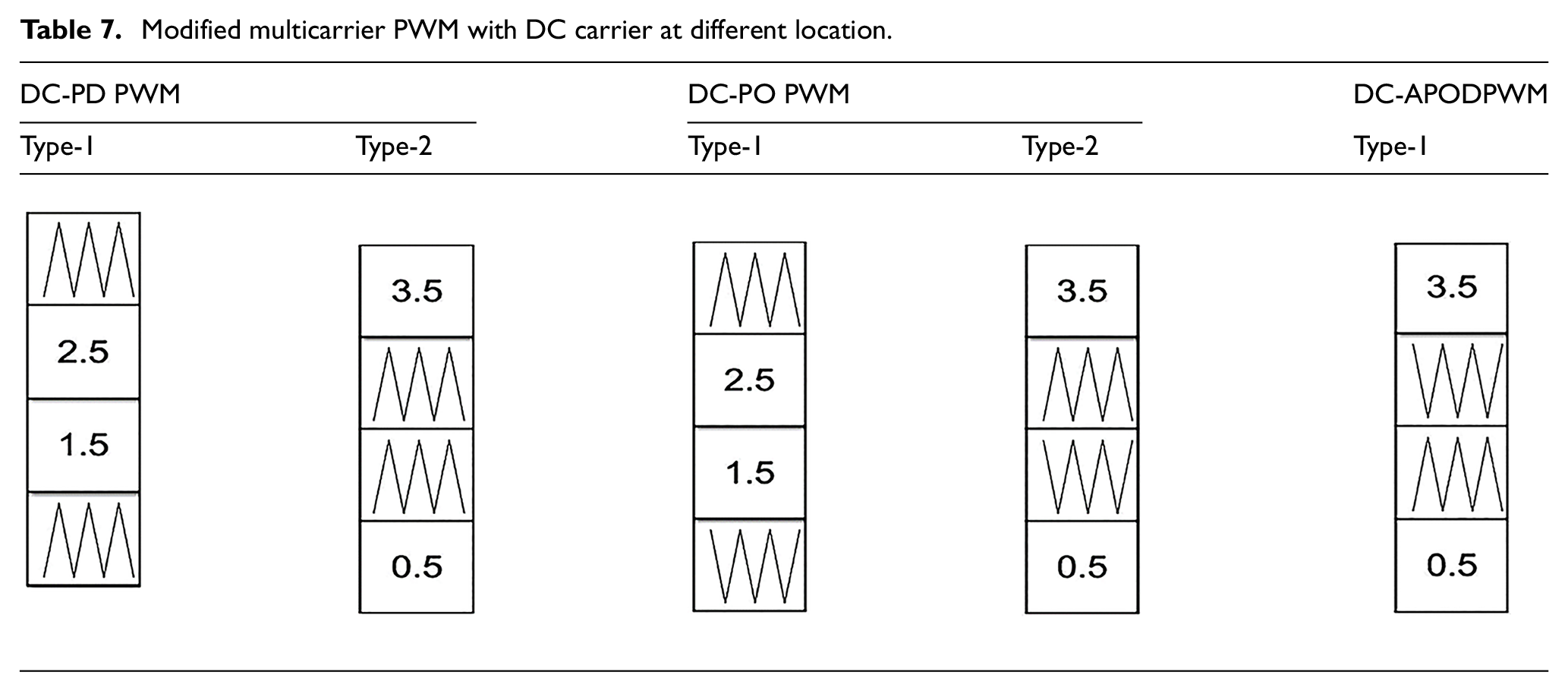
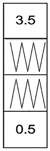
This paper suggests a modified Pulse Width Modulation (PWM) system that integrates Direct Current (DC) and triangular carriers across several carriers.Hence, Modified multicarrier PWM employs a mixture of triangular and direct current (DC) carriers) and enhances the efficiency and performance of Modular Multilevel Converters (MMC). The system has two direct current (DC) carriers and two triangular carriers, which are tuned for handling high-power applications and reducing switching losses. DC carriers offer more convenience in terms of implementation and control in hardware, whereas triangular carriers give improved harmonic performance and enhanced regulation of voltage levels. Through the reduction of switching frequency, this method effectively reduces switching losses without compromising control precision. The implementation of DC-PWM modulation technique decreases the frequency of switching and enhances the quality of voltage. This method guarantees the implementation of selective switching of sub-modules, hence minimizing unnecessary switching and power inefficiencies. When the magnitude of the sine wave above the minimum frequency of the carrier, a sub-module is inserted into each arm. When the magnitude of a sinusoidal waveform falls inside the range defined by the two lower and two higher carrier frequencies, two submodules are added. When the magnitude of a sinusoidal waveform drops below the maximum frequency of the carrier signal and surpasses the remaining three carrier frequencies, three sub-modules are introduced. Once the amplitude of the sine wave exceeds that of the carrier, all submodules are integrated. If the amplitude of all carriers exceeds that of the sine wave, all submodules are ignored. The number of submodules in both the upper and lower arms has a direct impact on the magnitudes of the produced voltages. When comparing direct current (DC) carriers to triangle carriers, several benefits become visible. Direct current (DC) carriers have a single potential value, yet this value represents an unlimited range of possibilities. As a result, it uses a considerably less amount of memory compared to other types of waveform data. Direct current (DC) carriers can be stored using eight bits. Nevertheless, it is crucial to acknowledge that triangular carriers comprising of 100 steps require a storage capacity of 100 multiplied by 8, resulting in 800 bits or, in other words, 100 bytes. The processing time is significantly reduced as compared to a waveform that contains a big amount of data points. If two out of four carriers are direct current (DC) carriers, the computation time can be decreased by a maximum of 20%. One significant advantage of using direct current (DC) carriers, as compared to conventional triangle carriers, is their relatively easier production and maintenance in hardware. The analysis of quarter wave symmetrical outputs is restricted to a certain group of many possible combinations. The presence of two direct current (DC) carriers is dependent on the existence of a single DC carrier at each respective location. There are two sets of DC carriers positioned in the middle, and a triangular carrier at both the highest and lowest points. The arrangement, which comprises of four carriers, is often known as Type-1. In Type-2, there are three sets of DC carriers: one at the top, one at the bottom, and one in the middle in the shape of a triangle.
The following are the main objective of work:
It is carried out investigation on the impact of the four submodule modules (SMs) in one arm of modular multilevel converter on the performance of DC-PDPWM modulation methods using a low cost STM32F407VG30,31 microcontroller and Op-amp base capacitor measuring and sorting circuit and the development of simplified methods to reduce computational burden and switching losses.
It is demonstrated conventional Phase-disposition (PD) pulse width modulation, modified multi carrier with direct phase i.e.DC-phase-disposition pulse width modulation type1 and type 2 (PDPWM) method for the five level MMC with a resistive load to assess its feasibility and effectiveness.
It is experimentally validated an efficient op-amp base sorting algorithm for balancing submodule capacitor voltages in modular multilevel converters with DC-PDPWM type-1 and type-2 for five level MMC with a resistive load to assess its real-world applicability, efficiency, and performance in high-voltage applications.
Section II provides an analysis of fundamental operations. Section III of the paper delves into the discussion of a modified level shift pulse width modulation approach. Section IV introduces a proposed modified phase disposition pulse width modulation (PDPWM) approach, wherein the conventional triangle carriers are substituted with DC levels. The evaluation and justification of the technique’s performance are conducted through simulation and an environment of experimentation.
Modular multilevel converter operating principle
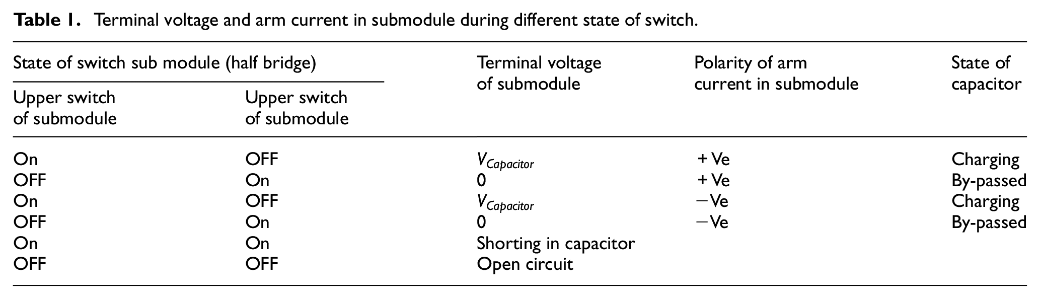
Figure 1 depicts MMC topological structure. This system is constructed of two bridge arms per phase with N identical SMs (plus an inductor) forming each of the bridge arms. The SM configuration consists of two Insulated Gate Bipolar Transistors (IGBTs), two anti-parallel diodes, and a direct current (DC) capacitor, as depicted in Figure 1. The name “sub-module” denotes a configuration consisting of two bidirectional switches, each equipped with antiparallel diodes and a DC capacitor.1–3 There exists a complementary relationship between these two switches, whereby Capacitor is either linked in the arm or bypassed. The capacitor functions as both an energy reservoir and a generation of voltage. The insertion of the sub-module into the arm circuit is carried out by the switches, while the antiparallel diodes are responsible for maintaining uninterrupted current flow. Given the similar nature of all the sub-modules, the operational concept of MMC may be applied to the operation at the cell level. The states of each sub-module are contingent upon the locations of the switches. In Figure 1(b), the sub-module is introduced into the circuit when switch S1 is in the ON state and switch S2 is in the OFF state. The sub-module is bypassed and the terminal voltage is zero when the lower switch is in the ON position and the upper switch is in the OFF position. The State of switch is tabulated in Table 1 as per terminal voltage and arm current in submodule. Based on the sub-module topology, it is necessary for the switches to function in a complimentary manner to prevent the occurrence of a short circuit in the capacitor. The voltage profile of the capacitor is influenced by the direction of the arm current. The red color is used to symbolize the supposed positive direction of the arm current, while the blue color is used to represent the negative direction. Upon the insertion of the sub-module, the positive current will initiate the charging process of the capacitor, traversing the top diode, whereas the negative current will result in the discharging of the capacitor. The capacitor voltage remains constant when the sub-module is bypassed. The two most prevalent forms of operation for sub-modules are insertion and bypass states. In the insertion condition, there is a possibility for upper IGBT or lower IGBT to experience the passage of upper IGBT or higher diode arm current. The primary circuit is electrically linked to a direct current (DC) capacitor, and the voltage produced by the sub-module is a direct consequence of this connection. Under the condition where the top IGBT is in a locked state, it is feasible for the arm current to pass via either the lower IGBT or the lower diode.
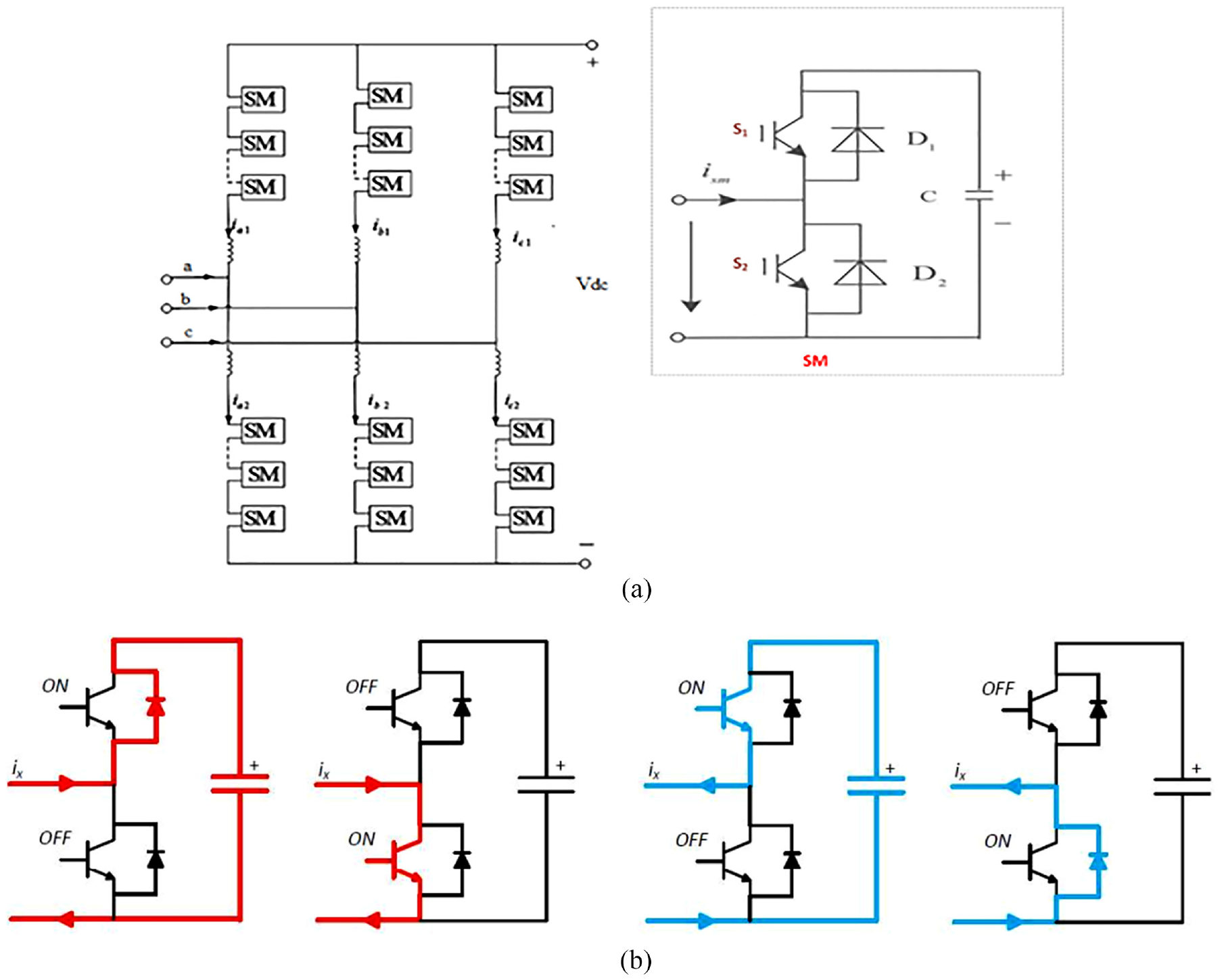
(a) Modular Multilevel converter (MMC) topological structure and (b) currents in submodule.
Terminal voltage and arm current in submodule during different state of switch.
The output voltage of the sub-module is zero due to the bypassing of the DC capacitor in the main circuit. The management of the switch states of the Insulated Gate Bipolar Transistors (IGBTs) enables the introduction or bypassing of submodules, irrespective of the direction of the current flow. Let N represent the quantity of bridge arms containing sub-modules within each arm. To maintain a consistent DC side voltage for each phase in the Modular Multilevel Converter (MMC), a strategy is employed wherein N sub-modules are introduced out of a total of 2N submodules at any one time. To clarify, the placement of N-non sub-modules is recommended in the upper arm, while non sub-modules should be positioned in the lower arm. It is generally advisable for each capacitor voltage value to remain in close proximity to its designated nominal voltage throughout operation. Nevertheless, under some situations, the voltages across capacitors might deviate significantly from the nominal voltage due to variations in capacitor value and the charging and discharging processes caused by arm current. Therefore, it is necessary to implement capacitor voltage balancing techniques in order to provide a consistent and equitable distribution of voltage across the capacitors. The utilization of the arm current effect is employed in the technique of capacitor voltage balancing. The inclusion of sub-modules including capacitors with relatively low voltage capacitance is recommended during periods when the arm current is positive, as this will result in the charging of the inserted capacitor. Consequently, the voltages across these capacitors with limited capacitance will increase during the charging process. In a similar vein, the incorporation of sub-modules exhibiting comparatively elevated voltages enables the reduction of said voltages in instances when the current flowing through the arm assumes a negative value, so facilitating the discharge of the capacitor that has been inserted. In the context of capacitor voltage balance sorting, the procedure can be outlined as follows: The capacitance voltages of a bridge arm can be measured and organized in either descending or ascending order. Additionally, monitoring the direction of the arm current can provide information on the number of sub-modules that should be inserted during the current sample period. The capacitance voltages of a bridge arm can be measured and organized in either descending or ascending order. Additionally, monitoring the direction of the arm current allows for the determination of the number of SMs that should be inserted during the current sample time. Based on the arranged voltage sequence and current direction, the appropriate non-submodule can be chosen. The voltage sub-modules, denoted as N-on, will be implemented when the arm current is positive. Conversely, N-non sub-modules will be employed when the arm current is negative. The subsequent section provides an elucidation of the operational mechanics of this particular methodology. The determination of the number of sub-modules that are introduced or bypassed is contingent upon the specific requirements of the application. An exemplification of this scenario would involve the establishment of voltage levels for four capacitors, specifically 72, 69, 73, and 74 V, with the selection of the capacitor with the lowest voltage for utilization. It is often advisable for individuals to possess knowledge regarding the sub-module with the lowest voltage. The utilization of hardware is essential for the implementation of this methodology. Operational amplifiers (op-amps) are employed in this technique to quantify capacitance. In this particular design, the capacitors within the sub-modules of a modular multilevel inverter are operating in a floating state. By implementing a gain reduction of 1/10 and establishing a common ground reference, the magnitude of the capacitor voltage is converted to the magnitude of the signal level. For instance, when the voltage across the capacitor is measured to be 76.4 V, the output voltage of the operational amplifier is found to be 7.64 V. The comparator integrated circuits (ICs) are utilized to compare the outputs of several operational amplifiers (op-amps) for the purpose of arranging the voltages across capacitors in either ascending or descending order. This arrangement follows a specific pattern, namely 1-2, 1-3, 1-4, 2-3, 2-4, and 3-4. The microcontroller is provided with six comparison results using signal level MOSFETs, level shifts, and current gain circuits. This enables the completion of the software execution of the capacitor balancing method. In the third phase, both arms are equipped with individual operational amplifier (OPAMP) and comparator integrated circuits (ICs), along with separate power supplies and voltage regulators. These components are utilized for the purpose of measuring and categorizing capacitors.
Level generation
The Modular Multilevel Converter (MMC) has the capability to produce a total of N + 1 levels or 2N + 1 voltage levels at its output. Here, N represents the number of sub-modules present in a single arm of the converter. In the context of N + 1 level generation, the total number of sub-modules inserted remains constant at N throughout the operation phase. However, in the case of 2N + 1 level generation, the total number of submodules inserted can vary between N − 1 and N + 1. Nevertheless, throughout a specified time period, the average number of inserted sub-modules is N. This section provides an explanation of the N + 1 level generation. In the case of a five-level modular multilevel converter (MMC), the total number of sub-modules in each arm is 4, denoted as N = 4. The equation provided represents the general expression for the output phase voltage. The variables
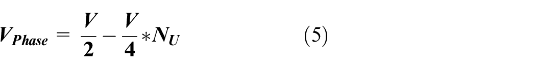
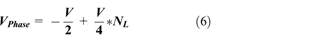
The relation between NU and NL is given by following equation.

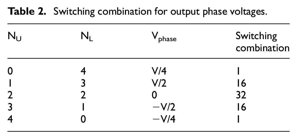
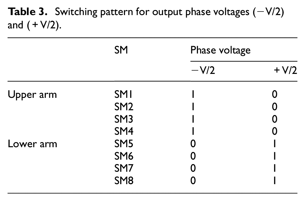
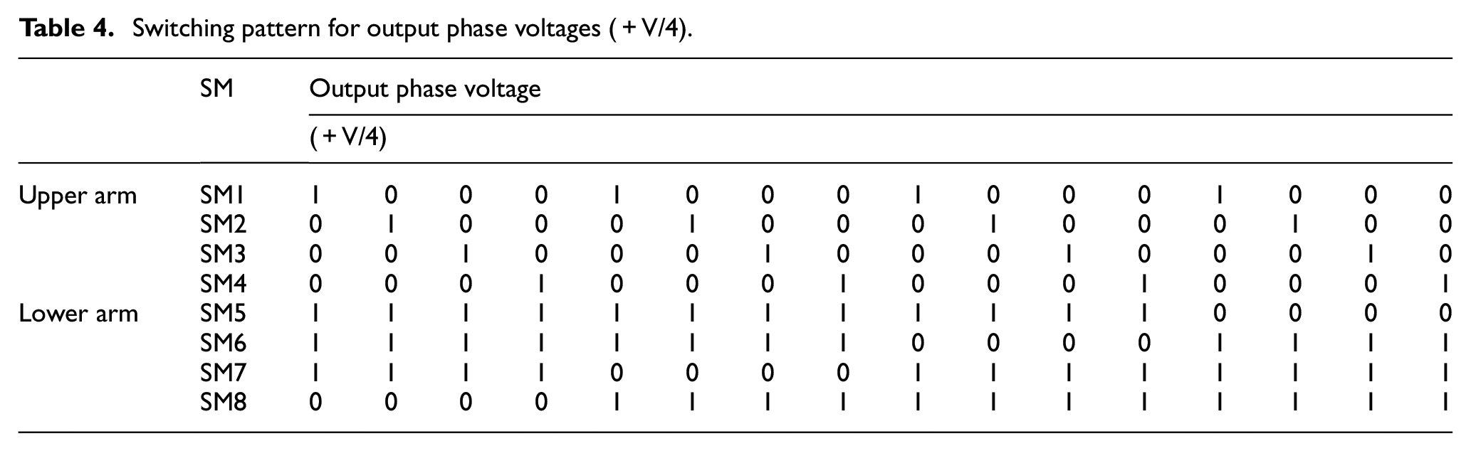
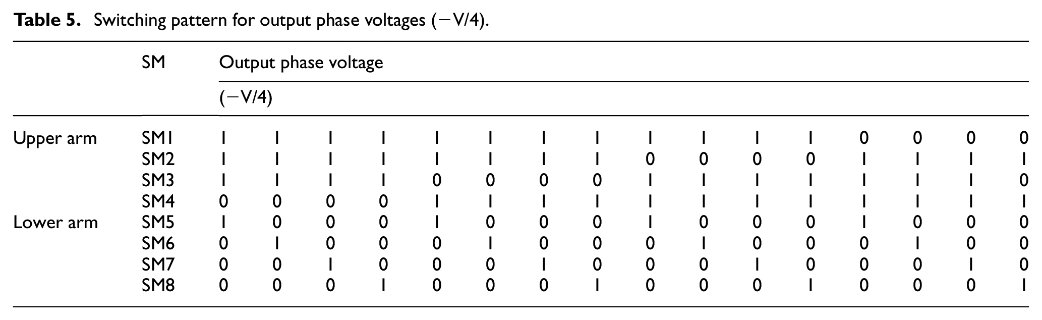
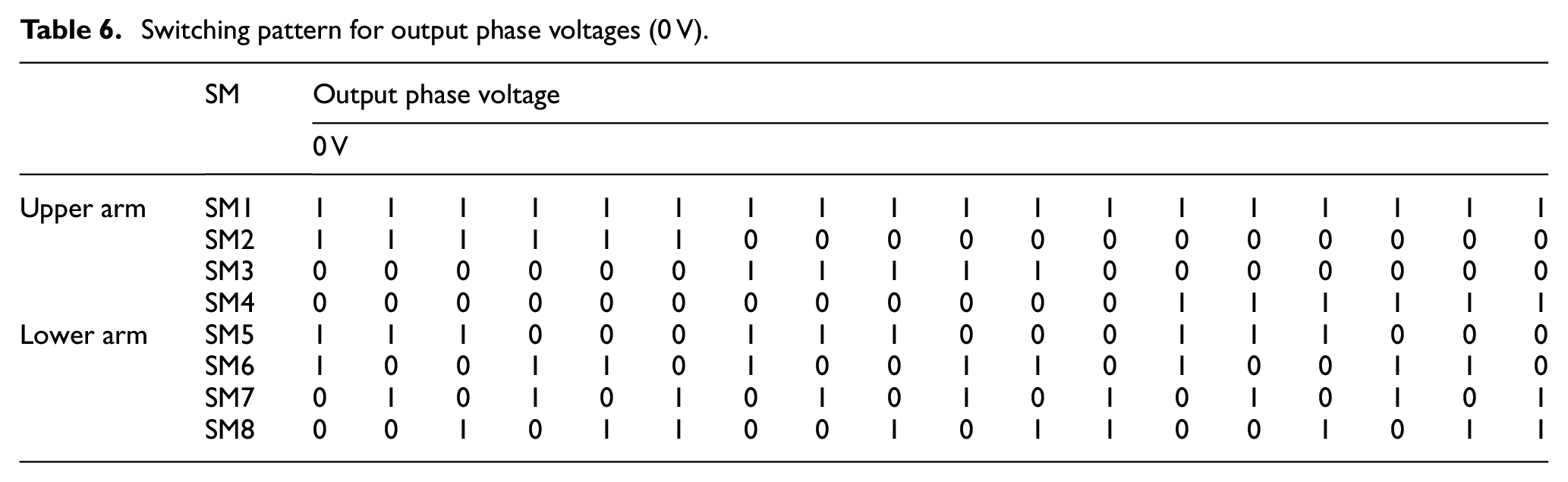
Tables 2–6 above present all possible switching combinations for each output phase voltage. The upper arm is comprised of sub-modules SM1–SM4, whilst the lower arm consists of sub-modules SM5–SM8. The value of 1 indicates that the sub-module has been inserted, while the value of 0 indicates that the submodule has been bypassed.The capacitor balancing algorithm is used to select the necessary possibilities from a given set of options.
Switching combination for output phase voltages.
Switching pattern for output phase voltages (−V/2) and (+V/2).
Switching pattern for output phase voltages (+V/4).
Switching pattern for output phase voltages (−V/4).
Switching pattern for output phase voltages (0 V).
Modified level shift pulse width modulation (PWM) technique
This section may be divided by subheadings. It should provide a concise and precise description of the experimental results, their interpretation, as well as the experimental conclusions that can be drawn.
Benefits of DC carrier over conventional multicarrier PWM triangular technique
This section introduces a multicarrier pulse width modulation (PWM) approach, which is tabulated in Table 7, and Figure 2(a), shows conventional PD-PWM. Figure 2(b)–(d) utilizes a combination of triangle and DC carriers. The reason lies in the DC carrier, as opposed to the triangle carrier. When the amplitude of the sine wave exceeds the minimum frequency of the carrier, a sub-module is introduced into each arm. When the amplitude of a sine wave is situated between the two lower and two upper carriers, two submodules are introduced. When the amplitude of a sine wave decreases below the highest carrier frequency and exceeds the remaining three carriers, three sub-modules are introduced. When the amplitude of the sine wave surpasses that of the carrier, all submodules are incorporated. When the amplitude of all carriers is higher than that of the sine wave, all submodules are disregarded. The quantity of submodules present in both the upper and lower arms directly influences the magnitudes of the generated voltages, as elucidated in the preceding section. In the context of modular multilevel converters, it has been observed that the utilization of five-level modulation results in a discernible phase disparity between the carriers of the upper and lower arms. In the context of nine-level modulation, it is seen that the upper arm carriers exhibit phase alignment with the lower arm carriers. When comparing direct current (DC) carriers with triangular carriers, several advantages can be seen. Although direct current (DC) carriers are characterized by a single potential value, this singular value encompasses an infinite spectrum of potentialities. As a consequence of this, it utilizes a significantly smaller amount of memory in comparison to alternative forms of waveform data. Direct current (DC) carriers have the capacity to be stored using eight bits. However, it is important to note that triangle carriers consisting of 100 steps necessitate a storage space of 100 times 8, which amounts to 800 bits or equivalently, 100 bytes. The processing time is greatly lowered when comparing it to a waveform that has a substantial number of data points. If two out of four carriers are direct current (DC) carriers, the calculating time can be reduced by a maximum of 20%. One notable benefit associated with the utilization of direct current (DC) carriers, as opposed to alternative waveforms, is their comparatively simpler creation and maintenance in hardware. Triangular carriers offer a range of applications for the utilization of DC carriers. The consideration of quarter wave symmetrical outputs is limited to a subset of numerous potential combinations. By employing the modulation technique described, it is possible to utilize either two direct current (DC) carriers or two triangle carriers (as depicted in Figure 2(d)), or alternatively, one DC carrier and three triangular carriers (as illustrated in Figure 2(b) and (c)), contingent upon their respective positions. The four-carrier modulation approach can be successfully implemented when there are precisely two direct current (DC) carriers, with one positioned in each upper and lower carrier location, and these carriers are synchronized. The presence of two DC carriers is contingent upon the existence of a single DC carrier in each respective place. There are two DC carrier sets located at the center, and a triangle carrier at both the topmost and bottommost positions. This configuration, consisting of four carriers, is commonly referred to as Type-1. In Type-2, there are two sets of DC carriers positioned at the topmost and bottommost positions, together with a triangle carrier located in the middle.
Modified multicarrier PWM with DC carrier at different location.
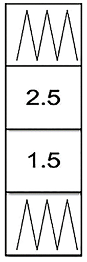
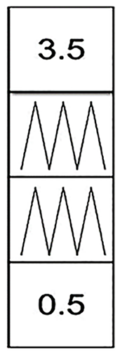
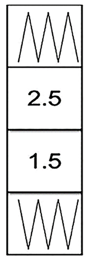
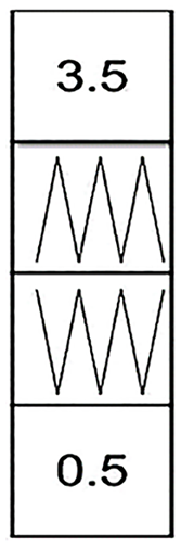
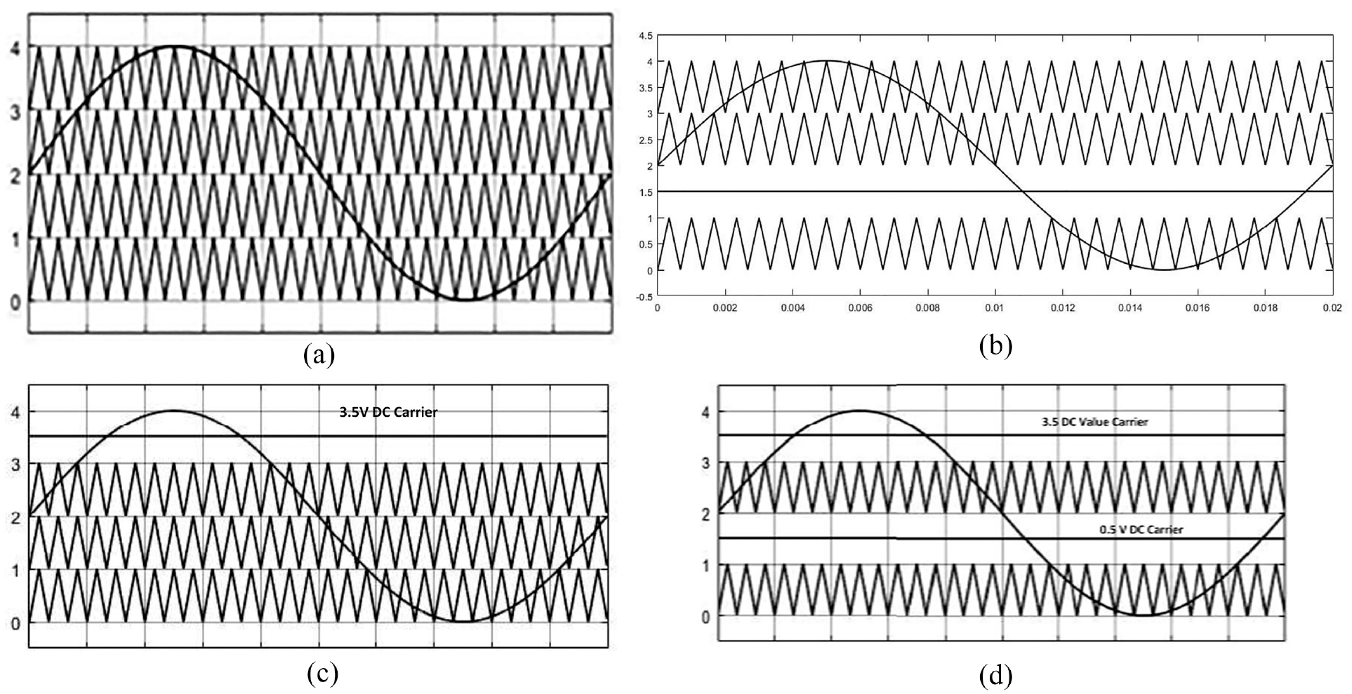
Pulse width modulation technique: (a) conventional phase disposition pulse width modulation, (b) & (c) one DC level shift multicarrier pulse width modulation, and (d) two DC level shift multicarrier pulse width modulation.
Capacitor measuring and capacitor sorting technique
The voltages of the capacitors are monitored using an Analog-to-Digital Converter (ADC) or using alternative methods that is, op-amp based circuitry. The capacitors are sorted based on their voltage, either through software or other hardware circuits. When there is a positive current in the arm, the switching technique determines the necessary number of sub-modules to be activated, selecting those with the lowest voltages. If the current in the relevant arm is negative, the sub modules with the greatest voltages are chosen according to the specified number. In the sorting method, capacitors are turned on or off at a specific frequency, even if the output state remains unchanged. The power losses in the reduced switching frequency method can be minimized by selectively switching the sub-modules only when there is a need to change the output state. The estimation technique involves computing an equation to determine the capacitor voltage, rather than directly measuring it. This approach is used to minimize the number of voltage sensors and reduce hardware complexity. A capacitor balancing algorithm is implemented in each phase, resulting in a total of three algorithms. The random module selection technique is employed in a specific phase, with a predefined frequency. In this particular methodology, there is no requirement for additional hardware. In this strategy, a specific frequency is utilized to incorporate the necessary quantity of submodules at regular intervals. At any one time, only a single sub-module is either inserted or bypassed. In the second phase, a random module selection mechanism is employed, whereby the state of all sub-modules is altered alone when there is a change in the output voltage level. The method exhibits a reduced switching frequency, resulting in less switching losses. In the third step, a novel approach for measuring capacitors and capacitor sorting technique them is implemented. According to the requirements laid out, a particular number of submodules are either included or excluded. Figure 3 shows op-amp based capacitor measuring circuits and sorting circuits. As an illustration, given a set of four capacitor values, specifically 72, 69, 73, and 74 V, the challenge at hand is to identify and put in the capacitor with the lowest voltage value. In order to maintain consistency with the lowest voltage sub-module, it is necessary to insert the second sub-module with a voltage of 71.9. This selection remains crucial. In general, it is necessary to possess knowledge on the arrangement of capacitors in either ascending or descending order. The precise magnitude of the capacitor is not necessary for our understanding. This technique requires additional hardware.
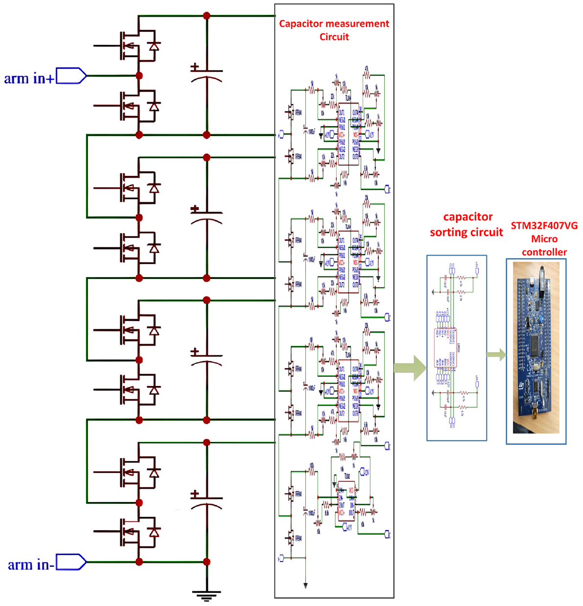
Op-amp based analogous capacitor measuring and capacitor sorting circuit interfaced with STM32F407VG microcontroller.
Op-amps are utilized in the measurement of capacitors. In the context of modular multilevel inverters, it is observed that the capacitors of all sub-modules are maintained at a floating level. The conversion of capacitor voltages to signal level magnitude occurs in a specific magnitude of capacitors. The gain of the system is reduced by a factor of 1/10, and all capacitor voltages are brought to a common ground reference. As an illustration, when the voltage across the capacitor is measured to be 76.4 V, the corresponding output voltage of the operational amplifier is found to be 7.64 V. The outputs of operational amplifiers are examined in different combinations, such as 1-2, 1-3, 1-4, 2-3, 2-4. In order to arrange capacitor voltages in ascending or descending order, it is common to utilize 3-4 comparator integrated circuits (ICs). These ICs are employed as a means of comparing the voltages and facilitating the sorting process. In the third phase, there are two arms, each equipped with its own separate capacitor measurement circuit consisting of operational amplifiers (OP-AMPs) and capacitor sorting circuit comprising comparator integrated circuits (ICs). These circuits are powered by isolated power supplies.
Op-Amp-based capacitor measurement and sorting algorithm
➢ • Begin the process of measuring capacitor voltages.
➢ • Use operational amplifiers to measure the voltage across each capacitor in the sub-modules. • Convert the capacitor voltage to a signal level magnitude (e.g. reducing by a factor of 1/10).
➢ • Store the output of the op-amp, which corresponds to the measured capacitor voltage (e.g. 76.4 V capacitor voltage results in a 7.64 V op-amp output).
➢ • Use comparator integrated circuits (ICs) to compare the capacitor voltages. • Comparisons are made between different pairs of capacitor voltages (e.g. 1-2, 1-3, 1-4, etc.).
➢ • Arrange the capacitor voltages in ascending or descending order based on the comparisons. • Ensure the lowest or highest voltages are selected for switching based on the arm current direction.
➢ • If the arm current is positive, activate the sub-modules with the lowest voltages. • If the arm current is negative, activate the sub-modules with the highest voltages.
➢ • Based on the sorted capacitor voltages, switch sub-modules on or off as required.
➢ • If a change in output voltage is detected, repeat the switching process. • If no change is detected, maintain the current switching state.
➢ • Continuously monitor and adjust the sub-module switching based on the capacitor voltage measurements.
➢
Results and discussions
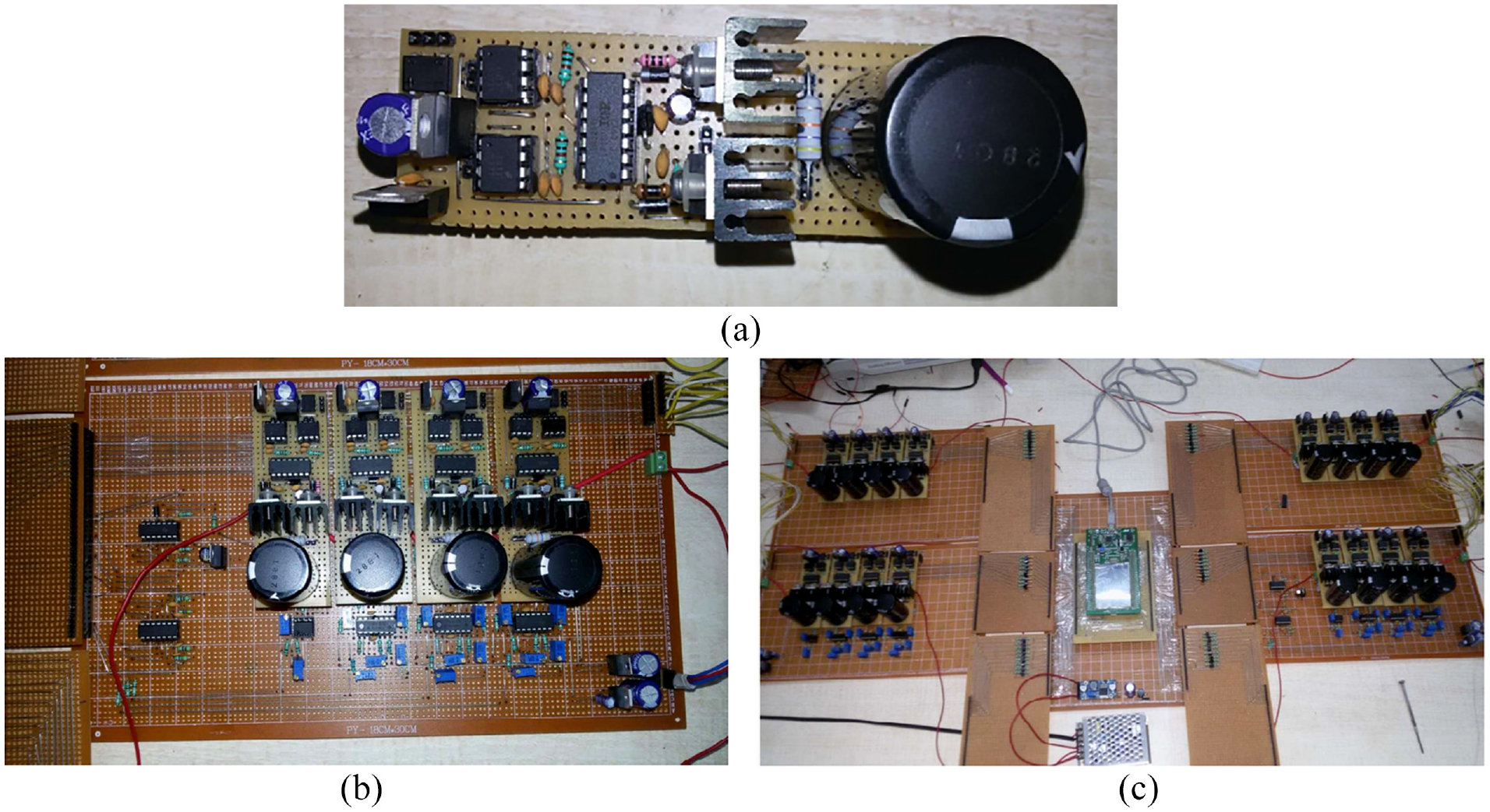
The simulation is carried out using MATLAB/Simulink, as shown in Figure 4. Different modulation techniques are used to replicate the five-level and nine-level modular multilevel converters (MMC) using four sub-module in one arm. The achievement of capacitor voltage balance is facilitated through the utilization of the sorting procedure, a technique that is employed in all methodologies. Table 8 provides parameters, which is utilized in the simulation.
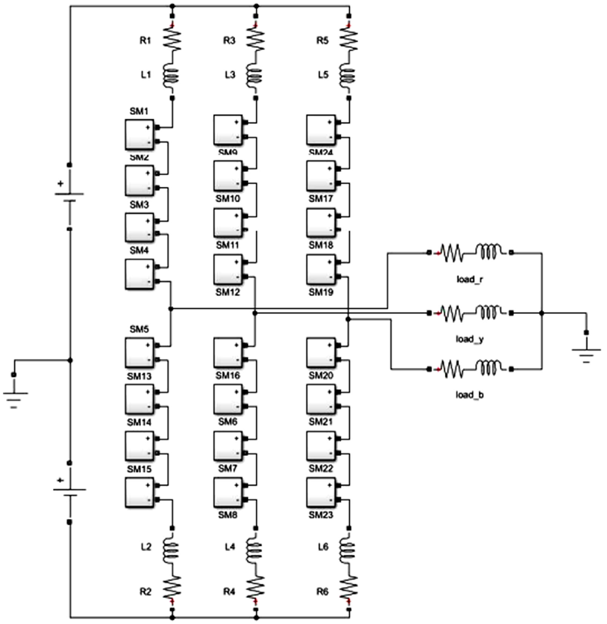
Simulation schematic circuit of MMC.
Simulation parameters.
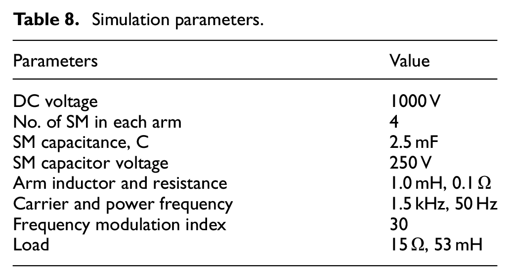
For DC-PDPWM techniques, two DC carriers are introduced in both type-1 and type-2 technique including %THD values of phase voltage, line voltage, phase current, and %ripple of capacitor voltage. Simulation results are obtained by using two DC level shift multicarrier pulse width modulation (Type-2) in five-level MMC with R-L load, as shown in Figure 5. The implementation of the power circuit in MMC hardware is achieved by a three-phase design.
Simulation results: (a) three phase line voltages, (b) phase voltages, and (c) line currents using two DC level shift multicarrier pulse width modulation (Type-2: PODPWM).
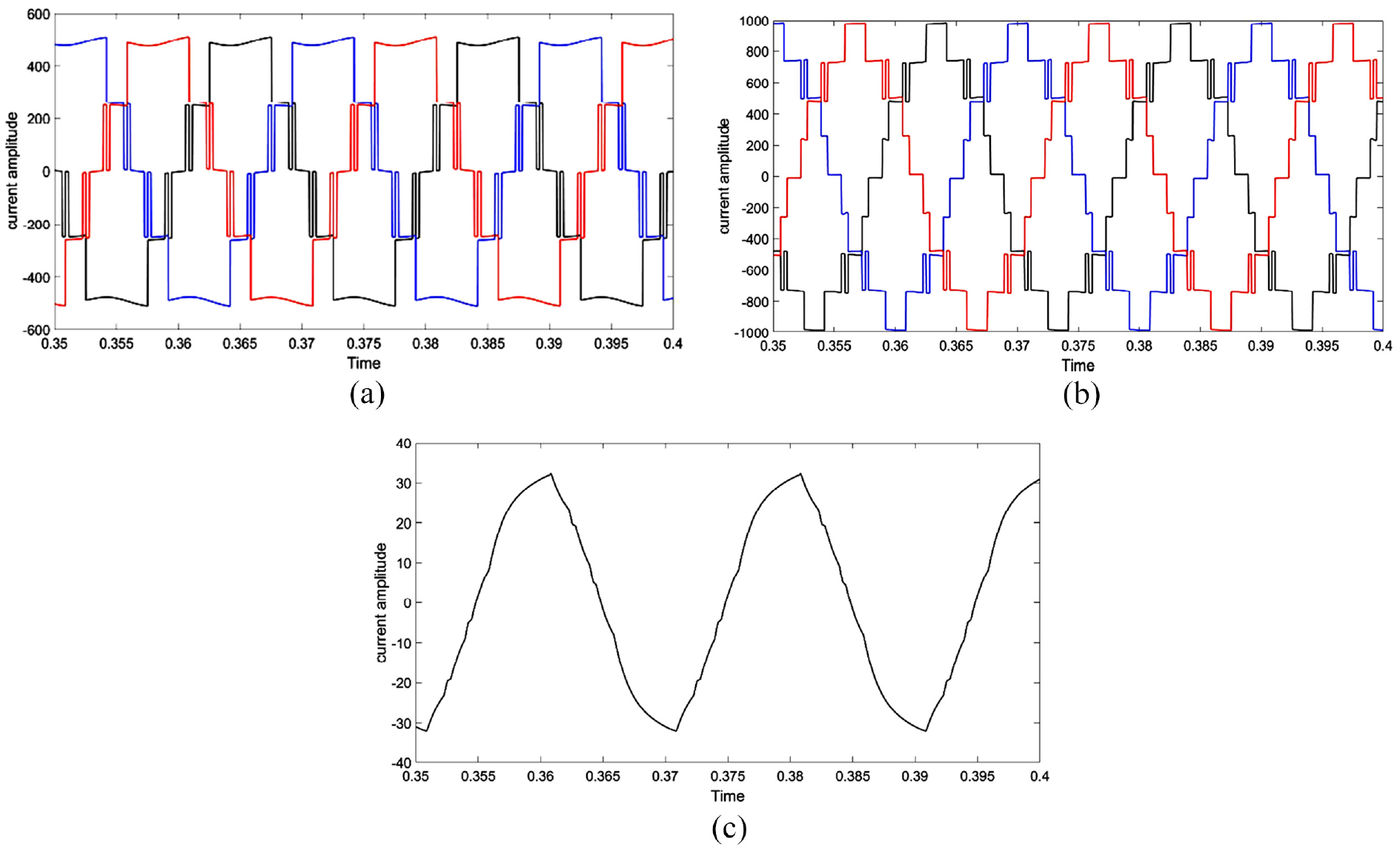
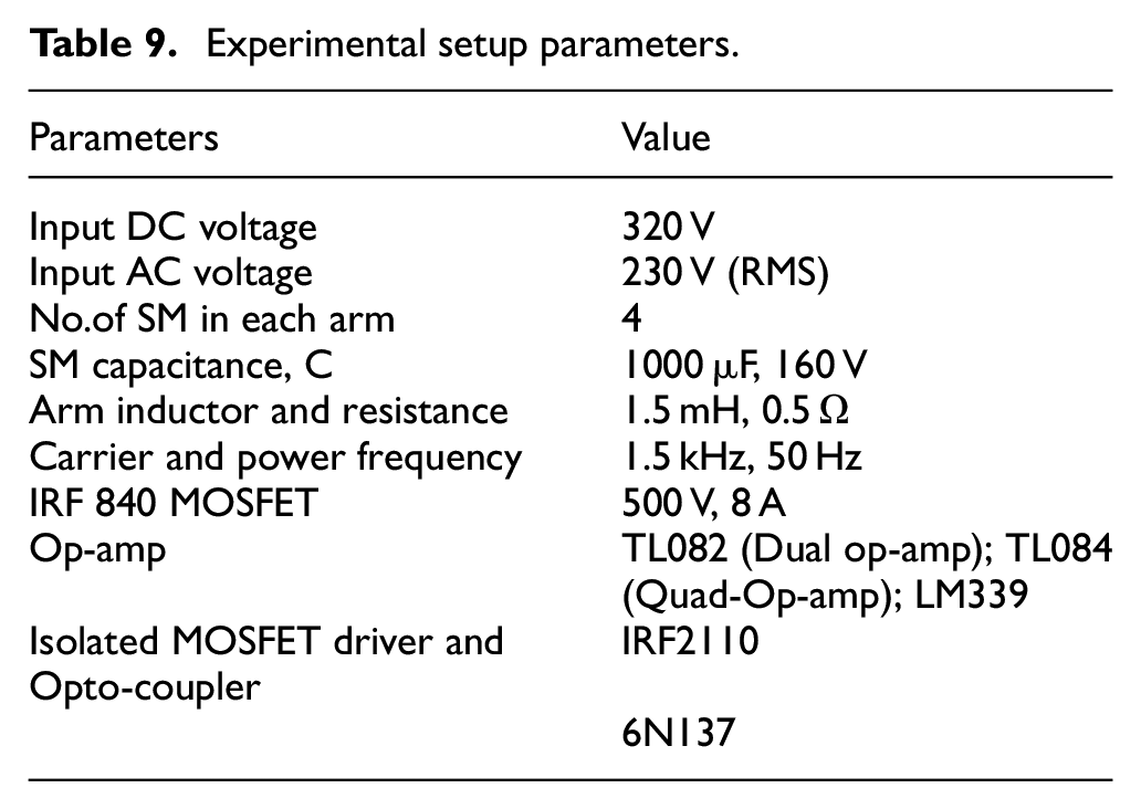
The real-time experiments setup is developed in laboratory as shown in Figure 6. Table 9 presents a comprehensive compilation of hardware parameters.
Experimental setup of modular multilevel converter: (a) switching module with signal processing circuit, (b) four switching module per arm modular multilevel converter, and (c) overall experimental setup with STM32F407VG microcontroller.
Experimental setup parameters.
The real-time performance of the five-level four submodule Modular Multilevel Converter with the Modified multicarrier PWM Technique was assessed by analyzing the voltage output under various modulation technique. Figure 7 illustrates the waveform of the converter Phase A and Line A output voltage using conventional PDPWM modulation technique, demonstrating stable and controlled voltage levels. Figure 8 illustrates the waveform of the converter Phase A and Line A output voltage using a DC carrier in multicarrier pulse width modulation (Type-1), showcasing steady and regulated voltage levels.
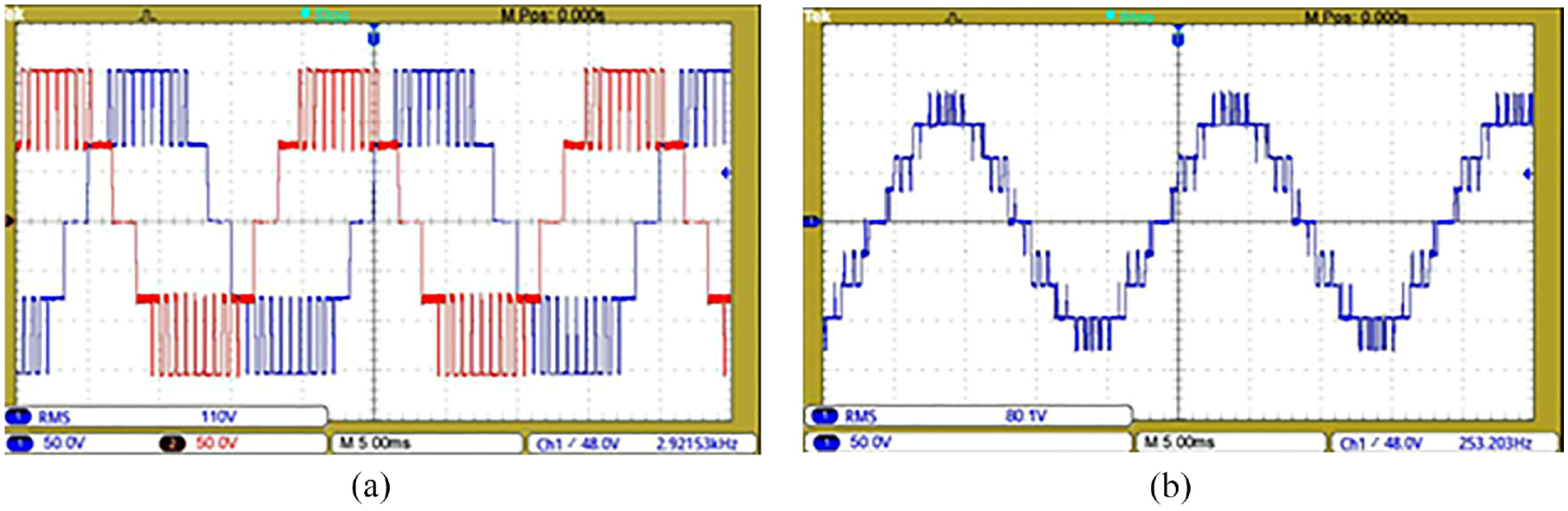
Experimental results: (a) Phase-A & Phase-B voltages and (b) phase-A line voltage of five-level modular multilevel converter using conventional PDPWM modulation technique.
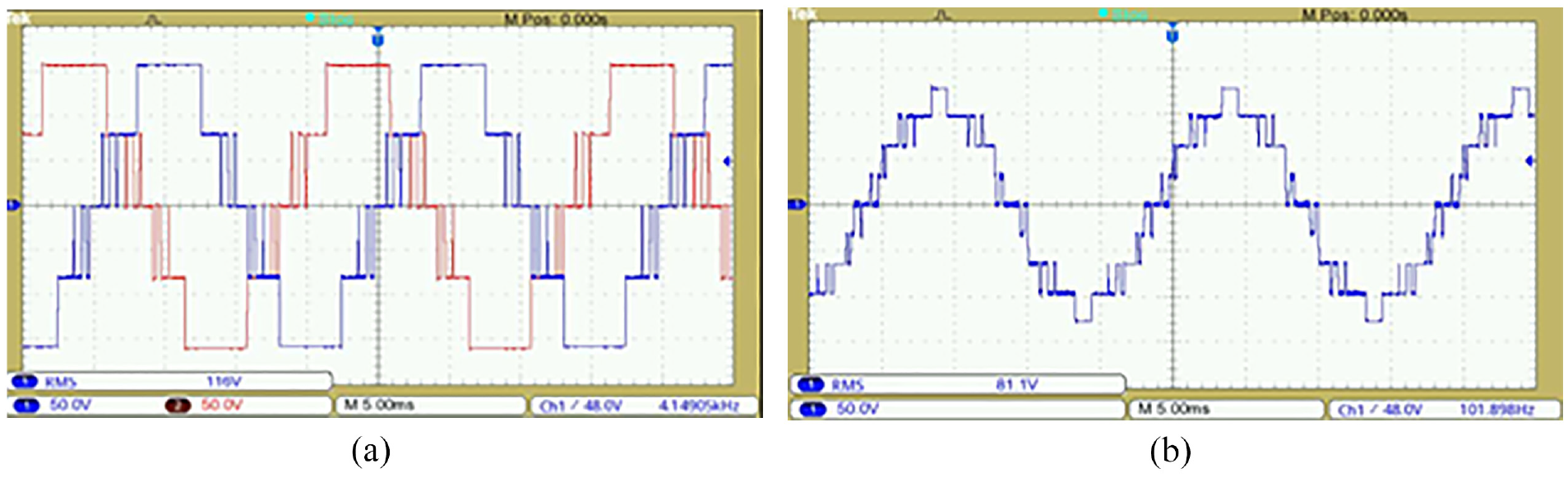
Experimental results: (a) Phase-A & Phase-B voltages and (b) Phase-A line voltage of five-level modular multilevel converter using one DC level shift multicarrier pulse width modulation (Type-1).
The converter Phase A and Line A output voltage waveform employing DC carrier in multicarrier pulse width modulation (Type-2) is shown in Figure 9, which shows steady and regulated voltage levels. The real-time experiments/simulations indicated the effectiveness of the Modified Level Shift Modulation Technique in achieving improved voltage stability. The impact of the Modified Level Shift Modulation Technique on switching frequency was investigated to assess its efficiency in minimizing power losses.
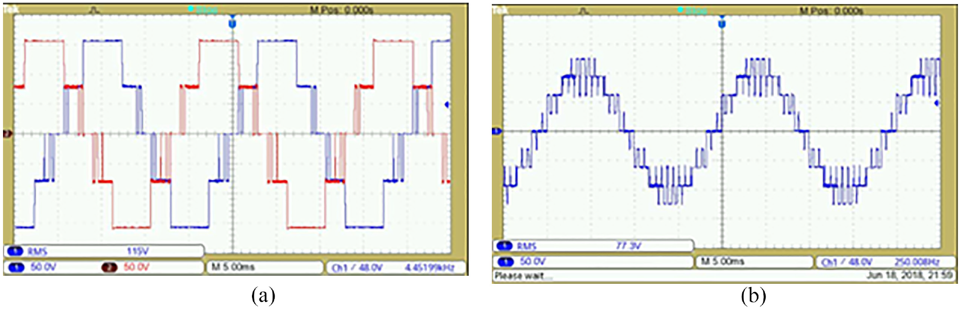
Experimental results: (a) Phase-A & Phase-B voltages and (b) Phase-A line voltage of five-level modular multilevel converter using two DC level shift multicarrier pulse width modulation (Type-2).
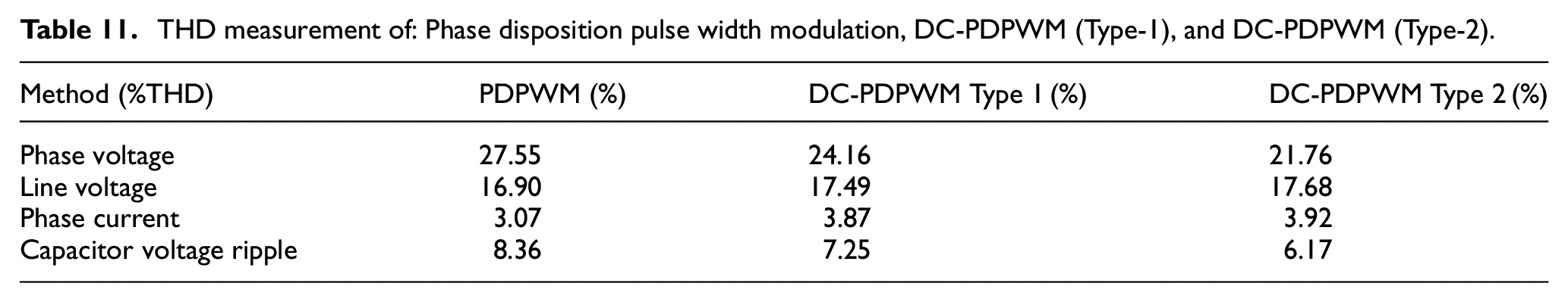
Experimental results provide a comparison of switching frequencies between the proposed technique and conventional modulation methods. The results demonstrate a notable reduction in switching frequency, indicating improved efficiency and reduced power losses. To evaluate the effectiveness of the Modified Level Shift Modulation Technique in reducing current ripple, real-time measurements were conducted. Tables 10 and 11 presents the current ripple across the resistive load, showcasing a significant reduction compared to conventional modulation techniques. The real-time results highlight the capability of the proposed technique to enhance the converter’s performance in minimizing current fluctuations.
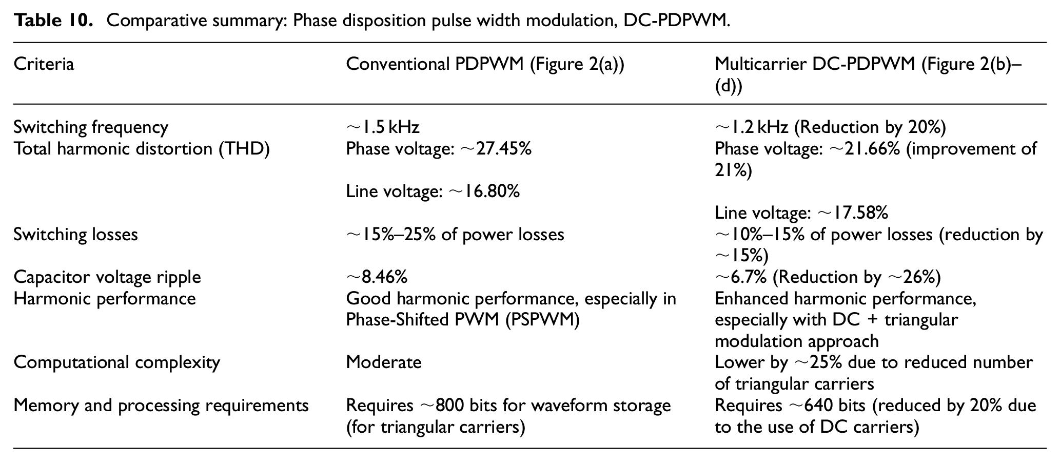
Comparative summary: Phase disposition pulse width modulation, DC-PDPWM.
THD measurement of: Phase disposition pulse width modulation, DC-PDPWM (Type-1), and DC-PDPWM (Type-2).
Conclusion
A simulation model is developed in MATLAB/Simulink to represent a three-phase Modular Multilevel Converter (MMC) with four sub-modules in each arm. The experimental setup incorporated modified multicarrier pulse width modulation technique that combined triangle and DC carriers. Among all the potential options, only those alternatives are chosen that yield a symmetrical output waveform in phase voltage and line voltage, namely with a quarter wave phase shift. The total harmonic distortions (THDs) of the selected approaches are comparable to or fall within the range of THD values observed in conventional methods. The hardware implementation involved a four submodule in arm Modular Multilevel Converter (MMC) configuration, with each arm consisting of four submodules. The total harmonic distortion (THD) of the hardware results and simulation results were compared, and it was seen that they were virtually identical. However, the hardware results exhibited a little greater THD due to factors such as line losses and switching losses. An op-amp based analogs approach for the measurement and sorting of capacitor voltages has been implemented. Among all the aforementioned combinations, the DC-PODPWM-type 2 exhibits the most favorable outcome, as it demonstrates the lowest total harmonic distortion (THD) in both phase and line voltage. The primary goal is accomplished by the utilization of operational amplifiers and comparators to eliminate the need for voltage sensors in the updated modulation process, hence reducing costs.
Footnotes
Declaration of conflicting interests
The author(s) declared no potential conflicts of interest with respect to the research, authorship, and/or publication of this article.
Funding
The author(s) disclosed receipt of the following financial support for the research, authorship, and/or publication of this article: This work was supported by the Dong-A University research fund.
Institutional Review Board Statement
Not applicable.
Informed Consent Statement
Not applicable.
Data Availability Statement
The data used to support the findings of this study are available from the corresponding author upon request.