
Abstract
This paper presents a phase-locked loop (PLL) based resonator driving integrated circuit (IC) with automatic parasitic capacitance cancellation and automatic gain control. The PLL consisting of a phase frequency detector (PFD), a loop filter, and a voltage-controlled oscillator (VCO) makes the driving frequency to be locked at the resonant frequency. The resonator is modeled by Butterworth–Van Dyke equivalent circuit model with motional resistance of 72.8 kΩ, capacitance of 6.19 fF, inductance of 79.4 mH, and parasitic parallel capacitance of 2.59 pF. To mitigate the magnitude and phase distortion in the resonator frequency response, it is necessary to compensate for the parasitic capacitance. The proposed automatic parasitic capacitance cancellation loop is operated in the open-loop mode. In the automatic parasitic capacitance cancellation phase, the outputs of the transimpedance amplifier (TIA) at the lower and higher frequency than the resonant frequency (VH and VL), are compared, and the programmable compensation capacitor array matches the VH and VL using binary-searched algorithm to cancel the parallel parasitic capacitance. The automatic gain control (AGC) loop keeps the oscillation at the suitable amplitude, and the AGC output can be used as a measurement of the motional resistance. The AGC loop is also digitally controlled. The proposed resonator driving IC is designed in a 0.18-μm bipolar complementary metal oxide semiconductor double-diffused metal oxide semiconductor (BCDMOS) process with an active area of 3.2 mm2. The simulated phase noise is −61.1 dBc/Hz at 1 kHz and the quality factor (Q-factor) is 59,590.
Keywords
Introduction
As the development of internet of things (IoT) technologies, various sensor markets are continuously growing. Recently, nanotechnology-based nanoresonator sensor is of interests to expected to have various sensor applications with the growth of the nano/microelectromechanical system (NEMS/MEMS) sensor market. By the motional resistance or motional inductance detection method of a nanoresonator, it can be used for measuring physical properties of liquid, such as density or viscosity,1–6 and it can be applied as bio sensors or chemical sensors that measure the blood glucose, and so on.
There are two main categories for the resonator driving system: open-loop system and closed-loop system. In open-loop system, resonant frequency and quality factor (Q-factor) can be obtained with the full frequency curve of a nanoresonator, 7 but the additional input driving source with frequency sweeps near resonant frequency is required. In the case of high Q-factor of resonator, the sweep size of the input frequency should be fine. With unknown resonant frequency, it can be difficult to find the resonant frequency depending on the frequency sweep range and size. Also, there are limitations in obtaining the continuous changes in Q-factor or resonant frequency. In closed-loop system, self-sustained oscillator8–11 circuit and phase-locked loop (PLL) architecture4,12 are mainly used. Compared to the oscillator circuit, PLL architecture has better adaptability to resonators and better performance with large damped resonators. 1
This paper presents PLL-based nanoresonator driving integrated circuit (IC) with automatic parasitic capacitance cancellation and automatic gain control. The nanoresonator was modeled by Butterworth-Van Dyke equivalent circuit model13–17 with motional series branch (resistance, inductance, and capacitance) and parallel parasitic capacitance. The purpose of the proposed nanoresonator driving IC is detection of the motional resistance, which is damping parameter of the mechanical lumped-parameter model. The nanoresonator model used in the proposed circuit has the motional series resonant frequency of 7.16 MHz, and the parallel capacitance of 2.59 pF. As the parasitic capacitance cause magnitude and phase distortions of frequency response and affect the resonant characteristic, the influence of the parasitic capacitance should be minimized. In this paper, a new method for the parasitic compensation is presented for the parasitic capacitance compensation. The automatic parasitic capacitance cancellation loop of the proposed nanoresonator driving IC automatically matches the programmable compensation capacitor array to the parasitic capacitance by using binary-searched algorithm, and compensate the parasitic capacitance properly.
PLL consists of phase frequency detector (PFD), loop filter, and voltage-controlled oscillator (VCO). PLL tracks the resonant frequency of the nanoresonator and keeps the oscillation frequency at the resonant frequency. The path through the AGC amplifier A3, resistor RREP and A4, which is the replica path with the path through the AGC amplifier A1, nanoresonator and TIA compensate the phase delay because of the AGC amplifier, nanoresonator, and TIA.
The automatic gain control loop (AGC)11,18 keeps the oscillation amplitude properly, by automatically tracking the set reference voltage VAGC. As the motional resistance can be obtained digitally by the AGC loop operation, the proposed circuit does not require an additional analog-to-digital converter (ADC).
The remainder of this paper is organized as follows. Section “Circuit implementation” describes the overall structure and compositions of the proposed scheme. Section “Circuit operation” describes the detailed operation principle of each mode (automatic parasitic capacitance cancellation loop, PLL, and AGC loop) of the proposed scheme. Section “Experimental results” shows the operation verification of the implemented circuit. The end of the paper concludes the proposed PLL-based nanoresonator driving IC.
Circuit implementation
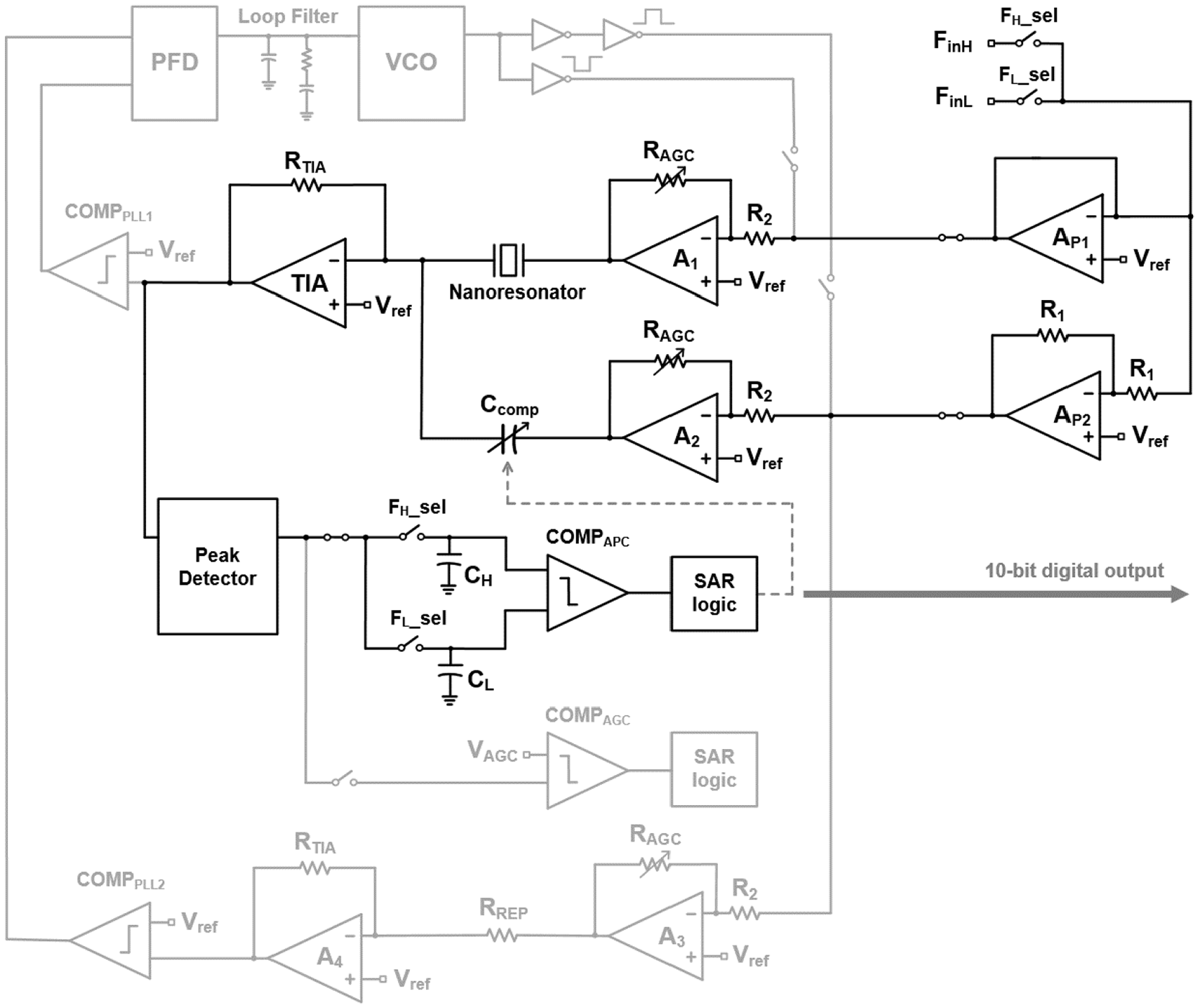
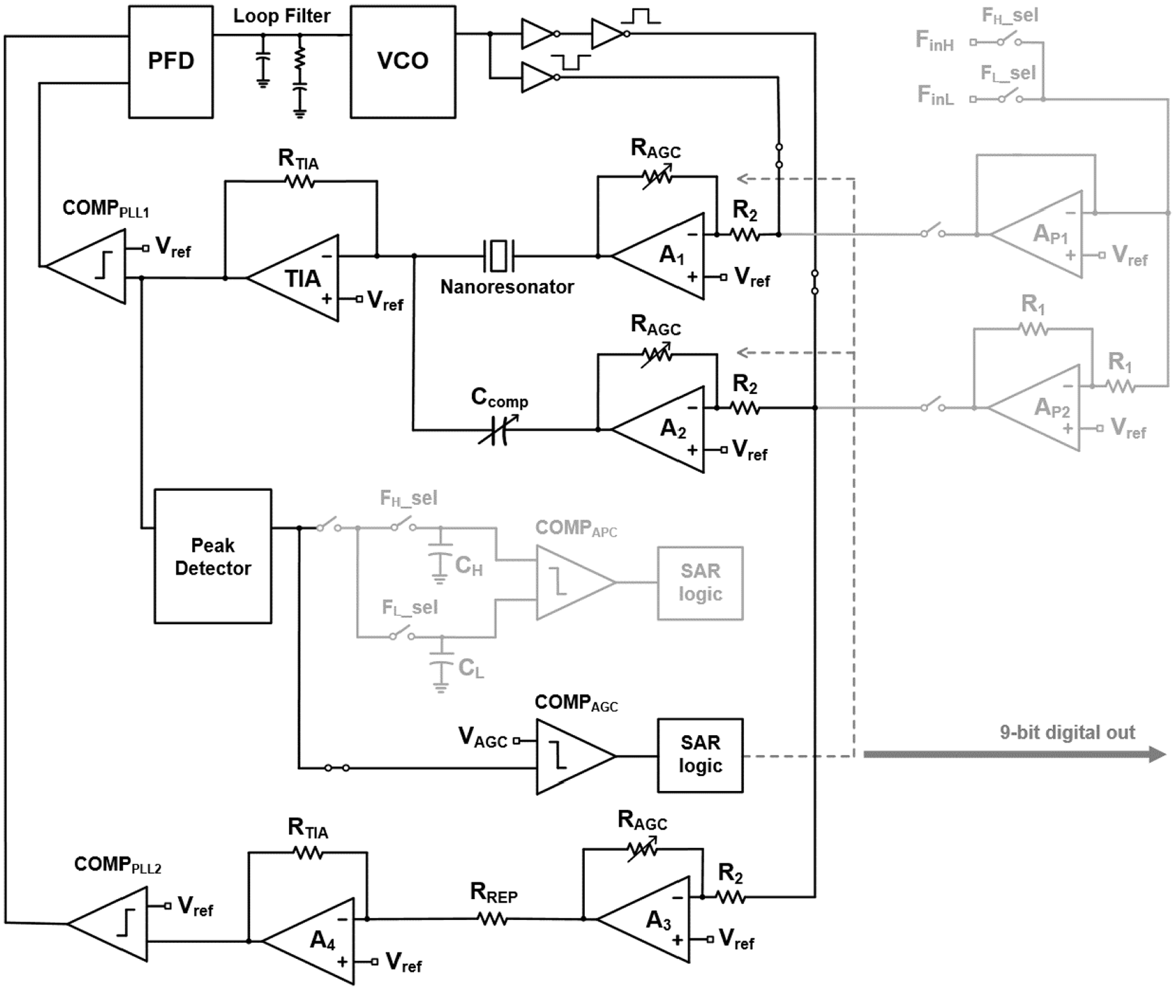
Figure 1 shows the top architecture of the proposed PLL-based nanoresonator driving IC with automatic parasitic capacitance cancellation and AGC. The automatic parasitic cancellation loop mode and the AGC loop mode can be selected by switching operation. Before the operation of PLL and the AGC loop, the automatic parasitic capacitance cancellation loop is activated first to compensate the parasitic parallel capacitance of a nanoresonator.
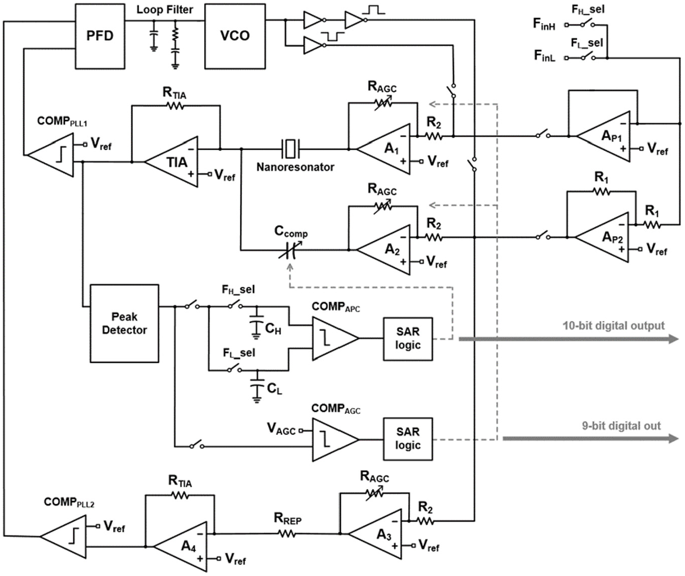
Top architecture of the proposed PLL-based nanoresonator driving IC with automatic parasitic capacitance cancellation and automatic gain control.
The automatic parasitic capacitance cancellation loop consists of 10-bit programmable compensation capacitors array Ccomp, buffer AP1, unity gain inverting amplifier AP2, TIA, peak detector, sampling capacitors CH and CL, comparator COMPAPC, and successive approximation register (SAR) logic. In the parasitic capacitance cancellation loop phase, a higher frequency and a lower frequency compared with the resonant frequency is implied to the input terminal FinH and FinL, respectively. By the sequential operation of two switches FH_sel and FL_sel, the circuit is driven in higher frequency and lower frequency sequentially. In the parasitic capacitance cancellation phase, RAGC and the gain of the AGC amplifiers (A1, A2, and A3) has a static value.
PLL consists of PFD, VCO, and loop filter. The phase of TIA output and VCO output are compared by two comparators COMPPLL1 and COMPPLL2, and PFD output that proportional to the phase difference controls VCO. The PFD output voltage is applied to the VCO and keeps the VCO output frequency at the resonant frequency. The AGC loop consists of 9-bit programmable resistor array RAGC, AGC amplifier, TIA, peak detector, comparator COMPAGC, and SAR logic register. The DC voltage input terminal VAGC at the comparator COMPAGC is the reference voltage that is compared with the peak voltage of the TIA output. The reference voltage VAGC can be arbitrarily set to a desired oscillation amplitude.
The nanoresonator model used in the proposed IC is shown in Figure 2. The nanoresonator was modeled by Butterworth-Van Dyke equivalent circuit model with the motional series resonant frequency of 7.16 MHz (the motional resistance of 72.8 kΩ, the motional inductance of 79.4 mH, the motional capacitance of 6.19 fF and the parasitic parallel capacitance Cp of 2.59 pF.
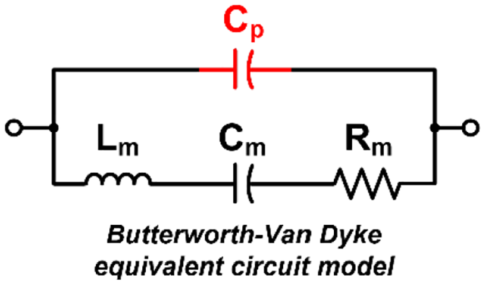
Butterworth-Van Dyke equivalent circuit model of the nanoresonator.
Figure 3 shows the charge pump PFD (CPPFD) 19 implemented in the proposed IC. The CPPFD is implemented with two D flip-flops, source current ISRC, and sink current ISNK. ISRC and ISNK which has the current value of 12 µA in the proposed circuit force the current into or out the loop filter. The loop filter is implemented with second-order passive loop filter with RLF of 600 Ω, CLF of 80 pF, and CF of 8 pF. The CPPFD compares the phase of VCO output and of TIA output, and locks the oscillation frequency at the resonant frequency of the nanoresonator. To avoid a dead zone region of the CPPFD, reset input is delayed using two inverter cells.
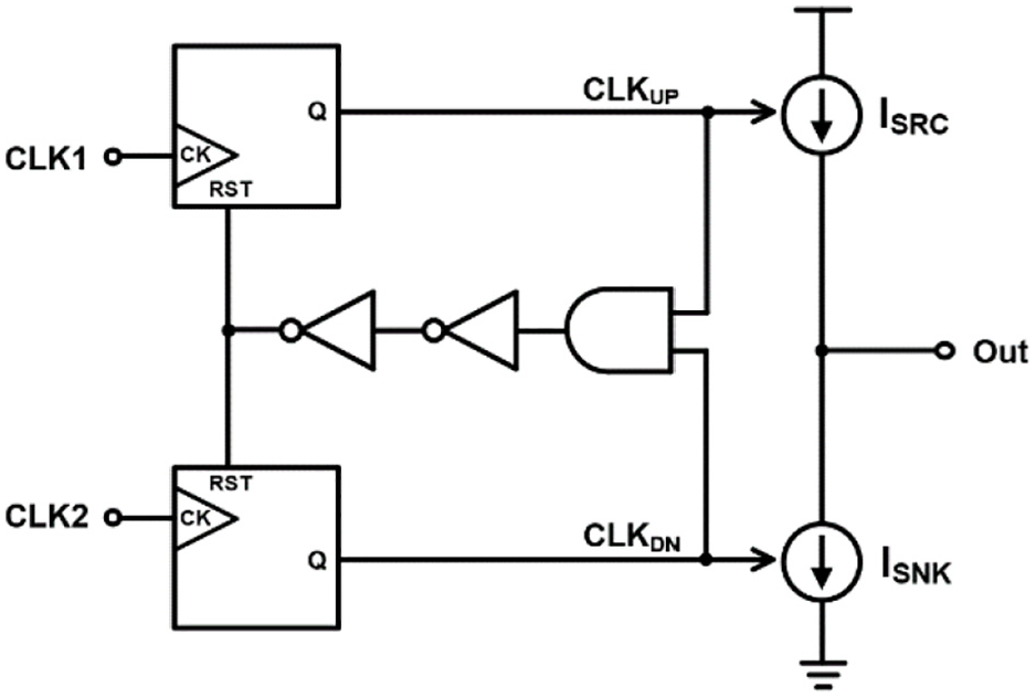
Schematic of the charge pump phase frequency detector (CPPFD).
Figure 4 shows the schematic of operational amplifier (op-amp) used in TIA, AGC amplifier, and peak detector. The op-amp is implemented with rail-to-rail folded cascode architecture and Monticelli’s class-AB output stage. 20 For the wide input range, M1–M4 forms rail-to-rail input stage. M9–M12, M17, and M18 constitute Monticelli’s class-AB output stage to achieve power efficiency. Cm1 and Cm2 is used to nested-Miller compensation capacitor to secure frequency response stability.
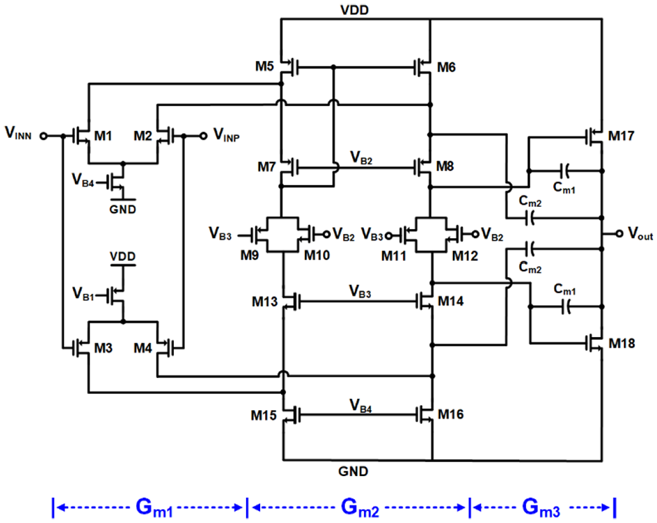
Schematic of the rail-to-rail folded cascode amplifier with Monticelli’s class-AB output stage.
Circuit operation
Automatic parasitic capacitance cancellation loop
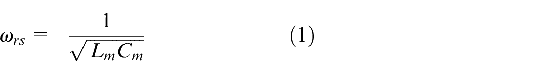
In the Butterworth-Van Dyke equivalent circuit model, the MSRF ωrs of the nanoresonator that parasitic capacitance Cp is ignored is expressed as:
In the case of Cp >> Cm, the parallel resonant frequency ωrp that Cp is considered can be expressed as: 16
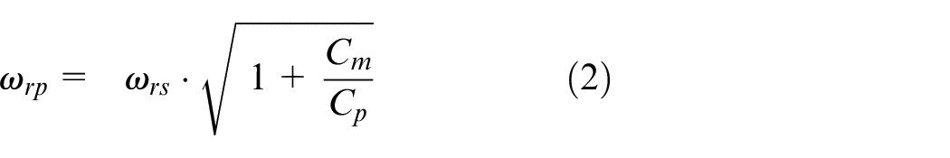
The equations (1) and (2) indicate that parasitic capacitance affect the frequency response of the resonator, and it should be compensated properly.
As shown in Figure 5, if the parasitic capacitance Cp is not compensated, the resonator no more has a band-pass filter characteristic having an accurate resonant frequency, and the gain continuously increases or decreases with the variation of frequency. By taking advantage of this these characteristics, the automatic parasitic capacitance cancellation loop operates by the method of comparing the output voltage by sequentially applying a low-frequency signal input and a high-frequency signal input compared to the resonant frequency.
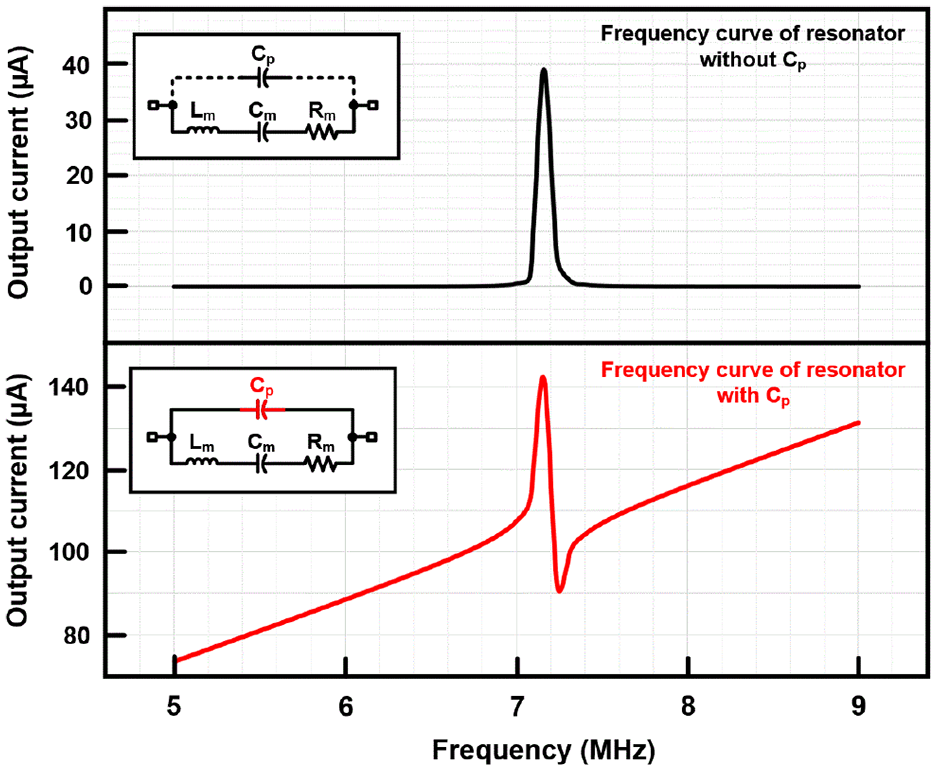
Frequency response of a nanoresonator with and without parasitic capacitance.
Figure 6 shows the connection status of the automatic parasitic capacitance cancellation loop mode. A high-frequency input and a low-frequency input is applied to the input terminals FinH and FinL, respectively and as shown in the timing diagram of Figure 7, the nanoresonator is driven in high-frequency input and low-frequency input sequentially by operation of two switches FH_sel and FL_sel. The nanoresonator and the compensation capacitor array Ccomp is driven with anti-phase by the buffer AP1 and the unity gain inverting amplifier AP2. The output current of nanoresonator driven in each input signal is converted to voltage and amplified by TIA, and each peak voltage of TIA output is stored in capacitors CH, and CL. The comparator COMPAPC compares voltage values stored in CH and CL, and the 10-bit programmable compensation capacitor array Ccomp is controlled by the method of binary-searched algorithm using 10-bit SAR logic register. This operation is repeated until the compensation capacitance Ccomp matches the parasitic capacitance Cp. Ccomp is driven in anti-phase to the nanoresonator driving input using unity gain inverting amplifier, and when Ccomp is equal to Cp, Cp is compensated.
Circuit connection status of automatic parasitic capacitance cancellation loop operation.
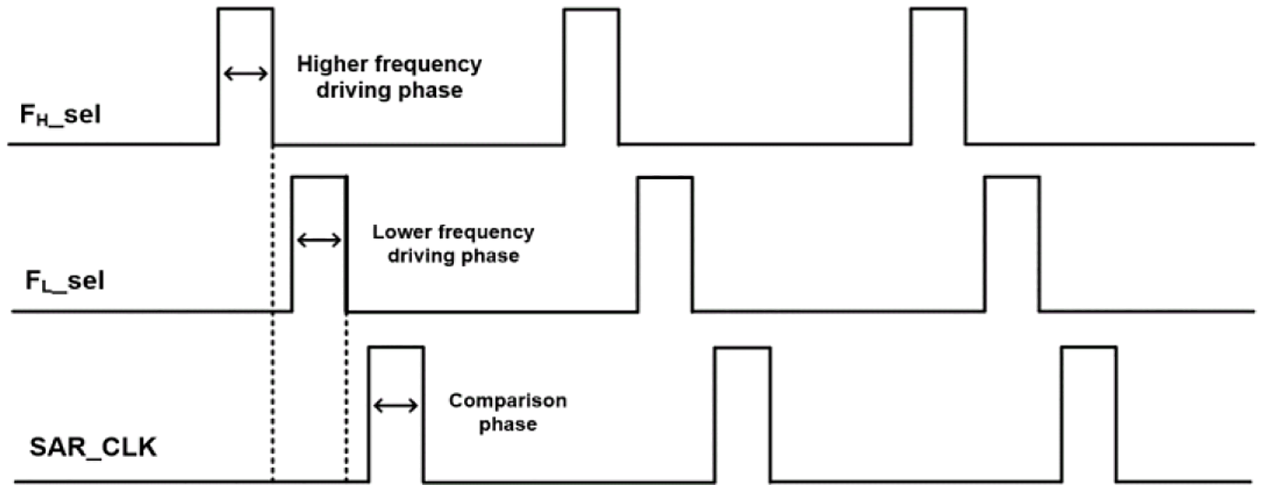
Timing diagram of automatic parasitic capacitance cancellation loop.
Figure 8 shows the conceptual frequency response of the nanoresonator during the automatic parasitic capacitance cancellation loop operation, and it briefly shows the process of matching the compensation capacitor Ccomp to the parasitic capacitance Cp. Before compensation, the initial frequency characteristic of the nanoresonator is shown as in Figure 5. As the automatic parasitic capacitance cancellation loop operates, the output at the frequency of FinH and FinL is compared and Ccomp is adjusted using SAR control. In this process, over compensation and under compensation of Cp is repeated, tracking the point where the gain at the frequency of FinH and FinL are same, that is, the point where Ccomp is matched to Cp.
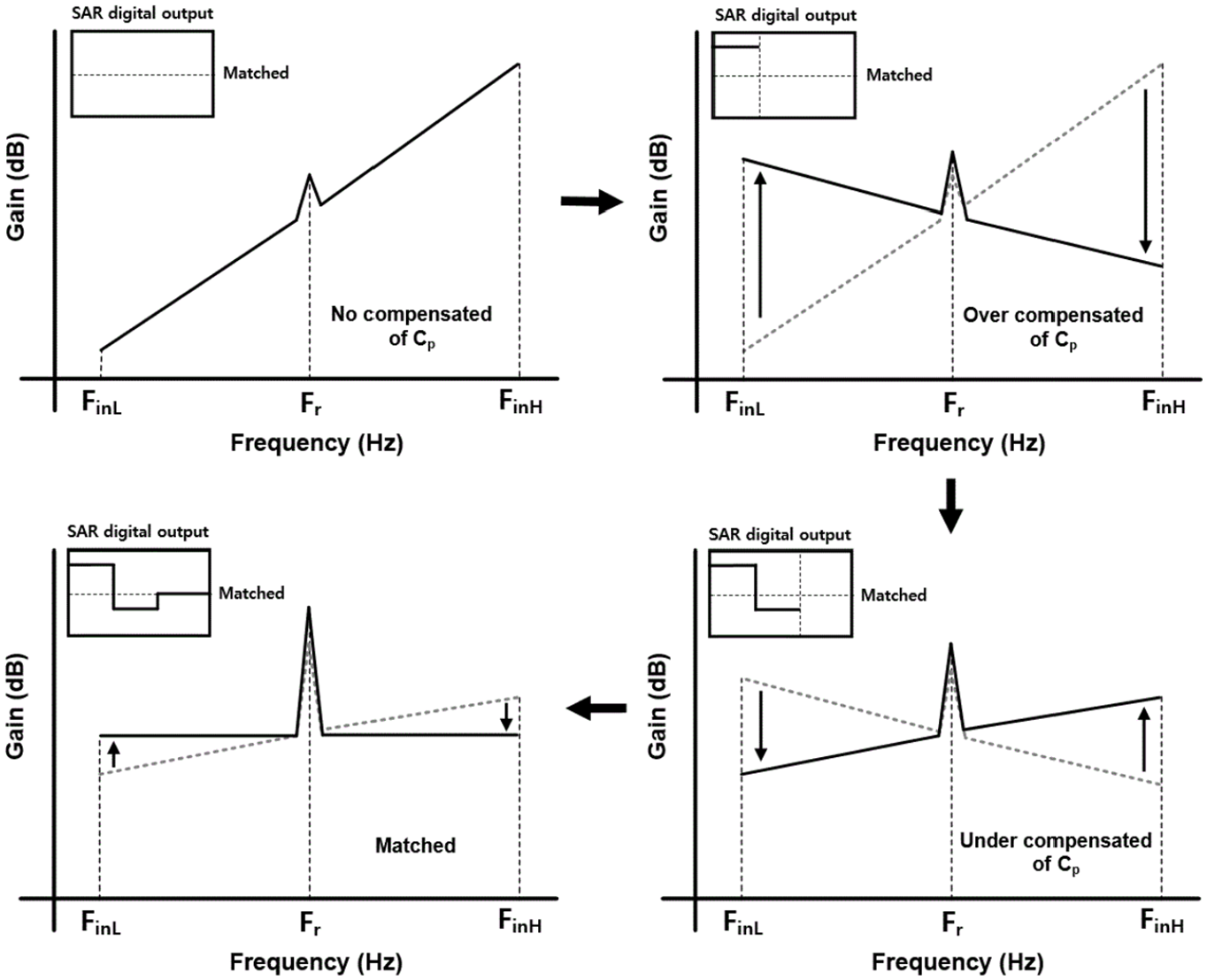
Conceptual frequency response of the nanoresonator during the automatic parasitic capacitance cancellation loop operation.
PLL and Automatic gain control loop
After the parasitic capacitance is compensated by the operation of the automatic capacitance cancellation loop, PLL, and AGC loop mode are activated. Figure 9 shows the connection status of PLL and AGC loop mode. The current output of the nanoresonator driven by VCO output is converted to voltage and amplified by TIA and the peak voltage of TIA output is compared to set reference voltage VAGC. The comparator COMPAGC compares the peak voltage of TIA output and VAGC, and 9-bit programmable resistor array RAGC is controlled by the method of binary-searched algorithm using 9-bit SAR logic register. As RAGC is controlled, the gain of the circuit is controlled and the peak voltage of the TIA output automatically tracks the reference voltage VAGC.
Circuit connection status of automatic gain control loop operation.
The motional capacitance Cm and the motional inductance Lm of the nanoresonator driven in resonant frequency are canceled each other out and if the parasitic capacitance Cp is compensated properly, the TIA output can be expressed as:
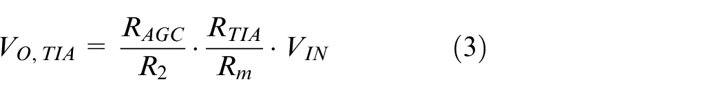
The motional resistance Rm can be expressed as:
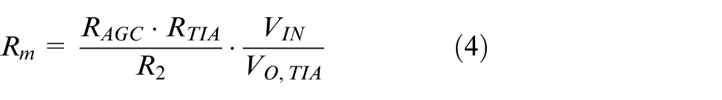
As shown in the equations, Rm can be obtained by RAGC, which can be obtained digitally from the SAR logic register.
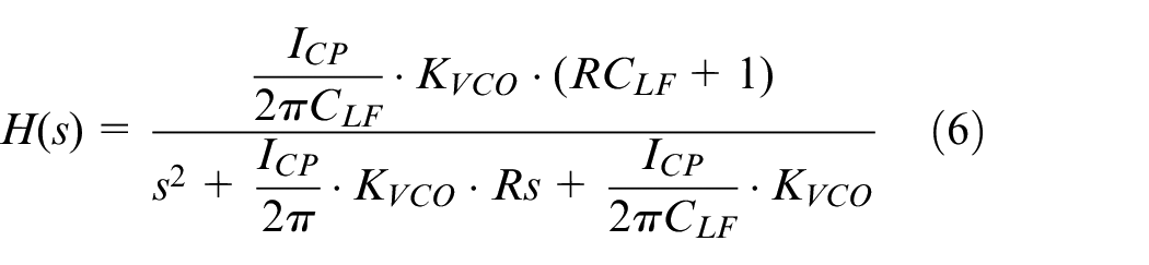
Assuming the nanoresonator as a narrow-band mechanical bandpass filter, the fundamental frequency of Vin is the natural frequency of the nanoresonator. The CF is about ten times smaller than CLF, the open-loop gain of the PLL can be approximated as:
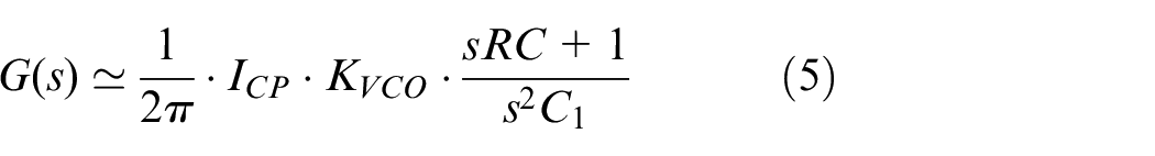
Where ICP is the charge pump current and KVCO is the voltage-to-frequency conversion coefficient of the VCO. Thus, the simplified closed-loop transfer function can be express as:
Experimental results
Figure 10 shows the layout of the proposed PLL-based nanoresonator driving IC with automatic parasitic cancellation and automatic gain control. The proposed IC is designed with a 0.18-μm bipolar complementary metal oxide semiconductor double-diffused metal oxide semiconductor (BCDMOS) process with an active area of 3.2 mm2.
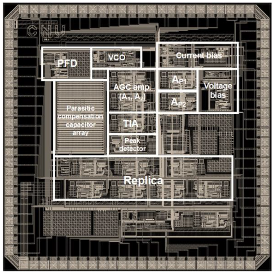
Layout of the proposed PLL-based nanoresonator driving IC.
The op-amp shown in Figure 4 is implemented with unit gain bandwidth (UGBW) of hundreds of mega-hertz to drive the nanoresonator model with the resonant frequency of 7.16 MHz. Figure 11 shows the loop gain simulation results of the op-amp. The op-amp has DC gain of 82.2 dB, and UGBW of 260 MHz, which is sufficient to drive the nanoresonator with 7.16 MHz of resonant frequency. The op-amp has the phase margin of 50° and secures the frequency stability.
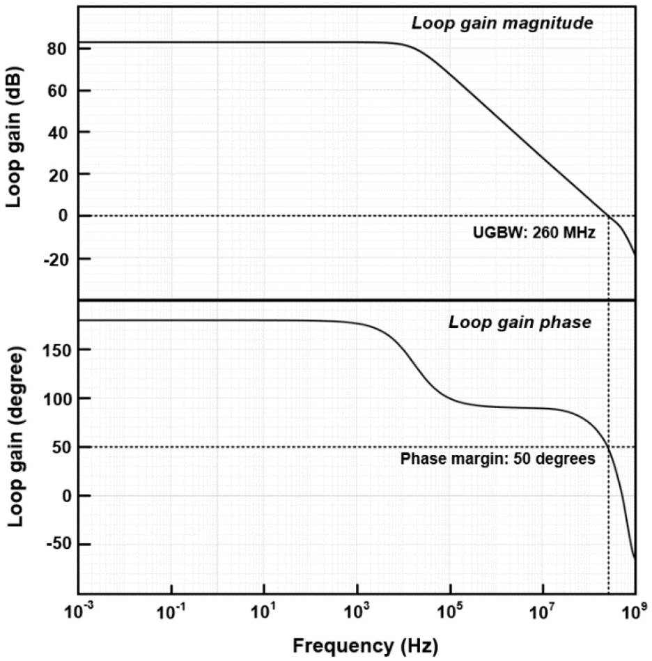
Loop gain simulation results of the rail-to-rail folded cascode amplifier with class-AB output stage.
Figure 12 shows the simulation result of the automatic parasitic capacitance cancellation loop. The 10-bit programmable compensation capacitor array Ccomp implemented with the unit capacitance of 33.4 fF matches the 2.59 pF of the parasitic capacitance Cp of the nanoresonator at digital register input of 76 or 77 in decimal. The SAR logic digital output controls the compensation capacitor array Ccomp, comparing the output at the frequency of FinH and FinL, as shown in Figure 8. The simulated SAR logic register digital output is 76 and the parasitic capacitance is compensated properly.
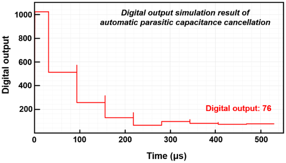
Digital output simulation result of the automatic parasitic capacitance cancellation loop.
Figure 13(a) shows the time domain simulation result of AGC loop when the motional resistance Rm is 10 kΩ, and the reference voltage VAGC is 1.2 V. The oscillation frequency is locked at 7.16 MHz, which is close to the resonant frequency of the nanoresonator. The peak detector output of the black line automatically tracks the reference voltage VAGC. Figure 13(b) shows the digital output of the AGC loop under the same condition and the simulated digital output is 13 in decimal.
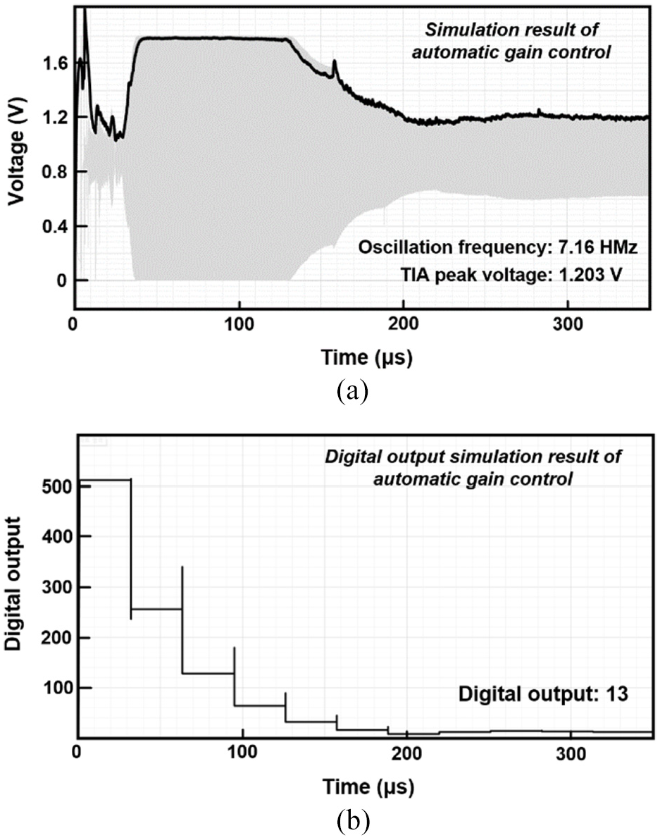
Simulation result of automatic gain control loop: (a) TIA and peak detector output and (b) digital output.
Figure 14 shows the motional resistance Rm detection simulation. Digital output of the AGC loop is simulated under the variation of the motional resistance Rm from 10 to 100 kΩ with intervals of 10 kΩ. The digital outputs for each resistance was non-linearity fitted with polynomial and digital outputs that vary linearly with the variation of Rm are obtained. The simulated non-linearity between Rm and digital output is 0.9% FSO.
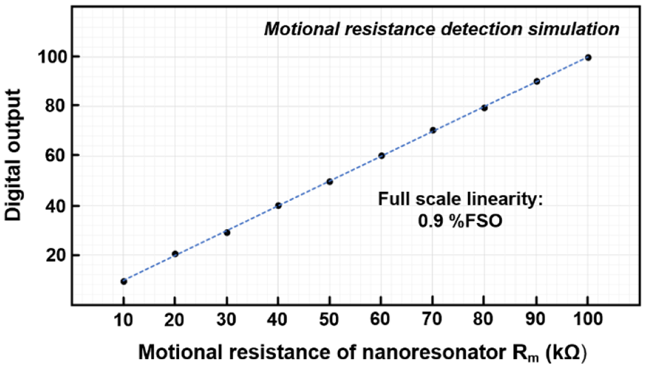
Motional resistance Rm detection simulation result.
Figure 15 shows fast Fourier transform (FFT) simulation result of the proposed PLL-based nanaoresonator driving IC when the motional resistance Rm is 10 kΩ, and reference voltage VAGC is 1.2 V. The proposed nanoresonator driving IC has 59,590 of Q-factor and −61.1 dBc/Hz of phase noise floor at 1 kHz offset.
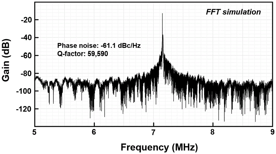
FFT simulation result of the proposed PLL-based nanoresonator driving IC.
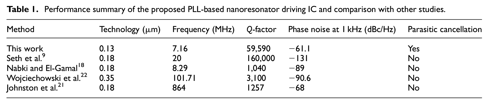
The performance of the proposed PLL-based nanoresonator driving IC with automatic parasitic capacitance cancellation and automatic gain control is summarized and compared with other method of driving resonator is shown in Table 1. As the parallel parasitic capacitance of the nanoresonator affects the frequency characteristics of the nanoresonator, the parasitic compensation included, and new method of automatically compensating for the parasitic capacitance is proposed.
Performance summary of the proposed PLL-based nanoresonator driving IC and comparison with other studies.
Conclusion
As nanotechnology-based sensor is expected to have various sensor application, nanoresonator can be applied as a bio/chemical sensor by the method of detecting the motional inductance or the motional resistance. This paper presents PLL-based nanoresonator driving IC with automatic parasitic capacitance cancellation and automatic gain control. The purpose of the proposed IC is to detect the motional resistance of a nanoresonator. To compensate the phase or the magnitude distortion of the frequency response, the parallel parasitic capacitance of the nanoresonator should be compensated. The automatic parasitic capacitance cancellation loop automatically tracks and compensate the parasitic capacitance of a nanoresonator by using binary-searched algorithm. The automatic gain control loop automatically tracks the reference voltage and control the gain of the circuit, and maintains the oscillation amplitude properly. The motional resistance can be detected by digital output of the AGC loop. As the proposed circuit does not require an additional ADC to obtain the motional resistance digitally, area and power efficiency can be achieved. The proposed IC is designed with a 0.18-μm bipolar complementary metal oxide semiconductor double-diffused metal oxide semiconductor (BCDMOS) process with an active area of 3.2 mm2. The simulated phase noise is −61.1 dBc/Hz at 1 kHz and the Q-factor is 59,590.
Footnotes
Acknowledgements
The EDA tool was supported by the IC Design Education Center (IDEC), Republic of Korea.
Declaration of conflicting interests
The author(s) declared no potential conflicts of interest with respect to the research, authorship, and/or publication of this article.
Funding
The author(s) disclosed receipt of the following financial support for the research, authorship, and/or publication of this article: This work was supported by the Electronics and Telecommunications Research Institute (ETRI) Grant funded by the Korean government (20ZB1155, Development of Core Technologies for Implantable Active Devices). This work was also supported by a grant to Bio-Mimetic Robot Research Center Funded by Defense Acquisition Program Administration, and by Agency for Defense Development (UD190018ID).