
Abstract
Solar energy exploitation through photovoltaic technology has demonstrated a sustainable way for curbing energy needs and cutting environmental issues happening due to emissions of carbon dioxide, CO2 from the usage of non-renewable energy resources. The purpose of this study was to reduce metallization by choosing optimal metallization on silicon photovoltaic wafer. Using numerical study, the effects of the number of busbars, fingers, and soldering/probe points were analyzed and also the study of the size of busbar and finger was carried out to find the optimal value for each which assures better performance. It is revealed that increasing the number and size of busbars, fingers, and probe points result in increasing fill factor, however, the efficiency of the device is limited to a number which provides the best optimal performance in terms of efficiency, whereas increasing the size (width) of the parameter result in a decrease in efficiency increasing shading factor. The optimal value of prescribed parameters was recorded as 4, 82, and 20 numbers of busbars, fingers, and probe points, respectively, while an optimal value of the width of busbar and finger is found as 0.5 mm and 60 µm, respectively. These values attained efficiency and fill factor above 20% and 80%, respectively. This study finds a realistic method to further diminish the metallization, improve the performance, and reduce the cost of often used industrial silicon photovoltaic cells.
Introduction
In recent days, renewable energy has emerged as one of the best possible solutions to cope up with environmental threats and ensure energy security at low production cost. All renewable resources could meet the desired needs of the energy sector with potential and availability all day; however, wind energy and solar energy are intermittent but have great potential to encounter. Solar energy is one of the cleanest sources of energy and assures sustainable development quickly with long-term stability in the supply market.1–3 Silicon wafer is often used for conversion of the Sun radiant energy into the electrical energy and requires the metallization sheet on the front and rear surface of the wafer to collect photo-generated current from respective surfaces and carry collected current to the external loads. 4 The conversion efficiency of the silicon photovoltaic (PV) cell is low (limited to 30% by Shockley) due to inherent properties of the silicon wafer itself and Sun radiations. Furthermore, efficiency decreases due to the metallic sheet provided for the current collection as it causes the optical (internal shading and reflective) and the electrical losses (resistive and recombination). Metallization sheet consists of the fingers which collect photo-generated current from the wafer and busbars which amasses current from the fingers and carries to an external load. Fingers are horizontal, and busbars are vertical metallic lines bars on the wafer surface and fingers are integrated with wafer while busbars are pasted on the surface of silicon wafer. 5 The shading due to the external or internal objects reduces the open-circuit voltage as well as operating voltage of the PV cell which in results contribute in the decrement of conversion efficiency of the device.6–8 The external shading greatly produces hot spots on the cell and generate multipeak results however internal shading does not have such damage on cell, but it shares the power loss of silicon PV cell. Furthermore, it has been revealed that shading also deteriorates the PV cell life cycle. 9 The external shading could also be eliminated using specific location and tilt angle while installing a PV system while internal shading requires to be worked on the design process of metallization. Therefore, to improve the performance of silicon PV cell, it is necessary to reduce metallization using optimal metallization on a wafer to achieve better performance from the device.
This paper introduces a numerical model attempts to reduce the losses happening in the silicon PV cell and improve the performance by optimizing the metallization pattern on it.
Conventional metallization pattern
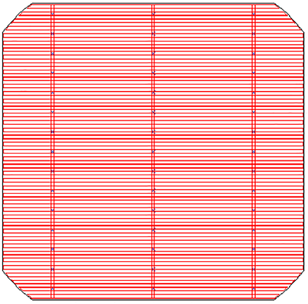
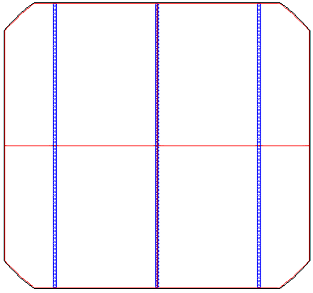
Industrial manufacturing companies often use the H-grid pattern as the current collection sheet for silicon PV cell which is the efficient pattern for squared and pseudo-squared PV cells; however, H-grid pattern does not perform efficiently in circular and polygonal-shaped PV cells. 10 It is named so because it looks like an English alphabet “H.” It is a front metallization pattern which requires metallic sheet on both sides, that is, front and rear which contributes in optical and resistive losses, however, the rear sheet does not contribute in optical losses while front metallization performs more in the current collection than rear metallization. Figure 1 shows an H-grid pattern metallization for silicon PV cell.
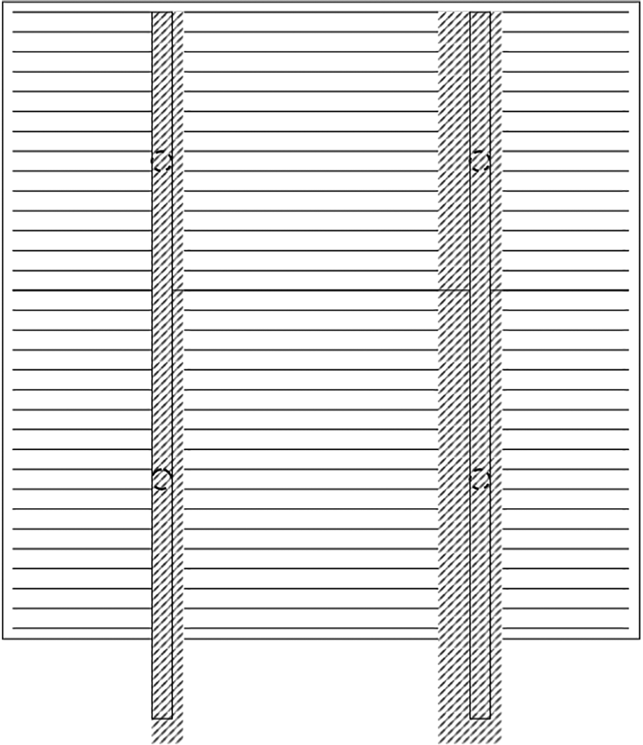
Visualizing fingers and busbars.
Though H-grid pattern performs better in squared or pseudo-squared shaped crystalline silicon PV cell and still it is required to reduce the metallization from front and back of the PV cell to reduce the optical and electrical losses more.11,12
This study focuses on diminishing fingers and busbars while increasing soldering/probe points (traced in Figure 1 by dotted circles) to achieve maximum performance from the device, as soldering/probe points are fixed behind the busbar hence not contributing in optical losses and also reduce electrical losses because of less metal usage.
Methodology
The important formulation used in modeling PV cell metallization is as follows
For current density

For voltage
where J is current density, Jlt is light generated, Jsc is short circuit, Jo saturation current density, q is an elementary charge, K is Boltzmann constant, T is absolute temperature, Rs and Rsh are series and shunt resistance, Voc is open-circuit voltage.
For fill factor (FF)
For efficiency
where FF is fill factor, Jmp and Vmp are current density and voltage at maximum power point, respectively, η is efficiency and Pin is power falling on cell.
Busbar calculation
Finger calculation
where Psb and Psf are the shadow fraction busbars and fingers, respectively, nb is the number of busbars, tb and tf are the effective transparency of busbar and finger, respectively. Wb, Wc, and Wf are the widths of busbar, cell, and finger, respectively, and S is the finger space.
Results and discussion
The structure of the PV metallization is created using AutoCAD. 13 The polyline function is used for the whole design creation beginning with creating wafer boundary than inserting fingers paired fingers and busbars simultaneously, finally drawing the soldering probe points on the busbars using circle function of the software. Various H-grid metallization designs are generated for the study, required for thorough study for optimizing metallization on the silicon wafer. Figures 2 and 3 show front and rear view of an H-grid metallization pattern, respectively. Dimensions of metallization used in this study are wafer boundary 156 mm × 156 mm and 180 µm thick, fingers and busbars are of the same length to wafer boundary, however their number and size are varied for the study while soldering points are of 0.5 mm diameter. Each design is saved in DXF format which is imported in Griddler2.5 for simulation and results generation. Griddler2.5 uses MATLAB compiler Runtime (MCR) for the calculations using following governing equations.14,15 This software is coded with programs which enable importing various designs of metallization from AutoCAD software in DXF format. Griddler2.5 software simulates metallization designs generating meshes and nodes of the metallization for solving a distributed network of resistors from both metallic sheet and the silicon wafer. After meshing, simulation is ready to generate current density–voltage (JV) curve, power–voltage (PV) curve, and detailed report of the simulation results.
PV cell metallization front view.
PV cell metallization rear view.
Influence of busbar on performance of PV cell
Figure 4 shows the effects of increasing busbar on efficiency and FF. It is observed that efficiency and FF gets a rapid increment from 17.4% to 19.3% and 69.3% to 78%, respectively, as the number of busbars is raised from 1 to 2 while further change in number of busbar results in augmenting FF to 81.06%, however, efficiency of cell have only small rise till 4-busbar getting as high as 19.58% then it drops to 19.22% when using 6-busbar in a cell. Drop-in efficiency of the PV cell is due to greater increment in the shading factor for the chosen number of busbars. It is noted that the optimal value of several busbars is 4 achieving the best optimal performance from a silicon PV cell.
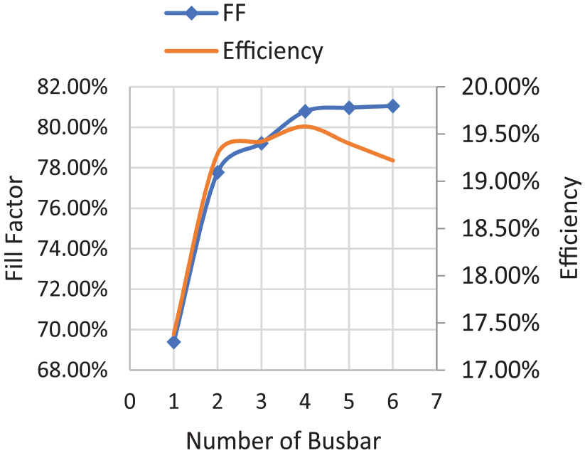
Influence of number of busbar on efficiency and fill factor.
Figure 5 illustrates the effect of busbar width on the performance of the PV cell. It is perceived that increment in busbar size augments the FF as wider busbar collects more current from the wafer active area, however, wider busbars also increase the passive area which limits the Sun radiations to be absorbed in wafer and generate current hence conversion efficiency of PV cell is decreased with increase in busbar width. Study finds that 4 mm addition in size reduces efficiency from 19.91% to 18.17% while the FF is raised from 80.34% to 80.49%. The optimal width of the busbar is found as 0.5 mm, however, thin busbars may further increase the conversion efficiency of PV cell.
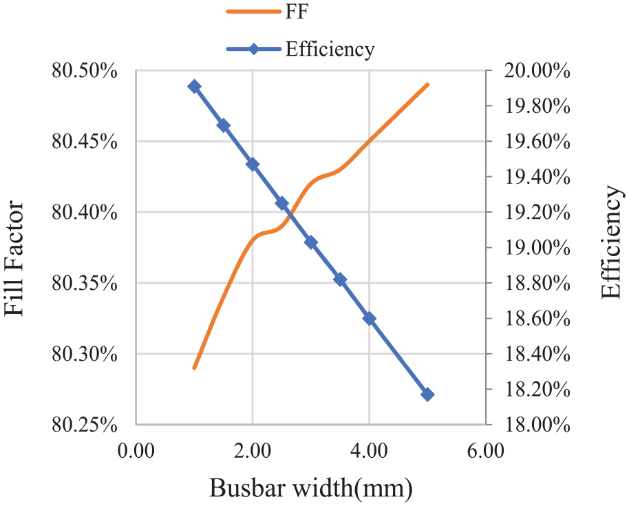
Influence of busbar width on efficiency and fill factor.
Influence of finger on the performance of PV cell
Figure 6 depicts the effects of the finger on the performance of the PV cell. It is observed that augmentation of fingers on silicon wafer results in increasing efficiency and FF of a cell, however, it is found that initial increment in both parameters is high and then they try to stabilize because of increment in shading caused by more increment in fingers. Efficiency rises from 6.51% to 19.49% while the FF begins from 37.75% to 80.09% when the number of fingers increased from 10 to 100. Optimal value fingers needed is recorded in range of 80–85 fingers per cell which gives the best optimal performance from the silicon PV cell.
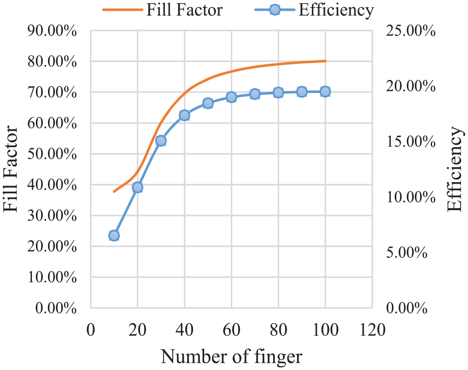
Influence of number of finger on efficiency and fill factor.
Figure 7 shows the effects of finger width on the performance of the PV cell. It is noted that increase in finger width improves the FF and efficiency of PV cell for a certain limit and then furthermore, augmentation in size of finger results in increasing in shading (passive area) which limits the radiations of Sun contributing in photocurrent generation causing decrement in the efficiency of cell, however, FF improves through the change in size. FF and curve of getting sharp growth from 60.14% to 79.92% when width increased from 15 to 135 µm while efficiency increases from 8.68% to 19.42% till 60 µm finger then it decreases to 18.69% for further change in the width of a finger. Study finds the optimal value of finger size as 60 µm which results in better performance from the silicon PV cell.
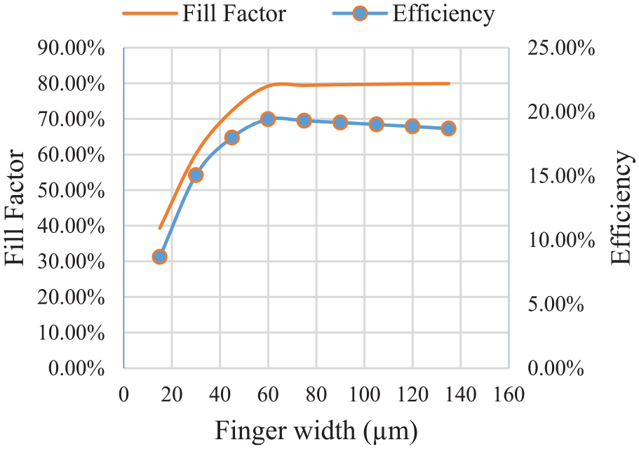
Influence of finger width on efficiency and fill factor.
Influence of soldering points on the performance of PV cell
Figure 8 depicts the effects of soldering/probe points on the performance of the PV cell. The study observes that augmenting probe points have a great influence on both efficiencies and FF of PV cell because probing increases the current collection from the wafer and not contributing in optical losses as probing is done behind the busbars. FF get high as 80.33% from 68.86% as soldering points increase from 1 to 60, however, the efficiency reaches to peak value 19.70% for 20 soldering points and for rest of increment it remains nearly unchanged. It is observed that the optimal maximum value of both parameters is achieved using 20 soldering points.
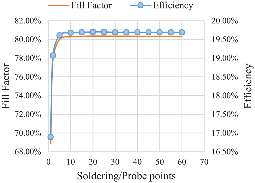
Influence of soldering/probe points on efficiency and fill factor.
Conclusion
This study is aimed to highlight the effects of metallization on the performance of silicon PV cell and optimize the metallization which should reduce the losses and improve the performance of silicon PV cell. A numerical study is performed using H-grid metallization pattern for finding optimal number and size of busbars, fingers, and soldering/probe points to be used for current collection purpose in a silicon PV cell. To find optimal number, busbars, fingers, and soldering points are studied in the range (1–6), (10–100), and (1–60), respectively, while the width of busbar and finger is varied in the range of 0.5–5 mm and 15—135 µm. Results reflect that increasing number has a great influence on FF, however, efficiency is improved for certain value and then it drops. The optimal number for metallization is recorded as 4-busbar, 82-fingers, and 20-soldering points; and optimal width is revealed as 0.5 mm and 60 µm for busbar and finger, respectively. This assures nearly 20% efficiency and FF above 80%.
Generally, it is concluded as thin busbars and fingers are more favorable than using a greater number of those for current collection which assures better efficiency as well as nearly same FF to that of using more fingers and busbars meanwhile 20 soldering points must be selected for silicon PV cell and arranged in regular order behind busbars.
Footnotes
Acknowledgements
The authors acknowledge the reviewers for providing valuable feedback to further improve this work.
Declaration of conflicting interests
The author(s) declared no potential conflicts of interest with respect to the research, authorship, and/or publication of this article.
Funding
The author(s) disclosed receipt of the following financial support for the research, authorship, and/or publication of this article: The authors are grateful to Huaiyin Institute of Technology and Jiangsu province (Grant No: JAS18022) for providing financial support to complete this project. This research was also supported in part by Natural Science Foundation of Jiangsu Province under contracts BK20161302 and State Grid Fundation of Jiangsu Corporation J2017123.
Data accessibility statement
The data used for supporting results of this study are included in this article.