
Abstract
The photovoltaic module testing apparatus being used presently for photovoltaic measurements acts principally on the method of photovoltaic module loading with resistive, capacitive, and electronic elements. In this work, a new method is described using a supercapacitor as the load to the photovoltaic module. This technique of characterization has proved to generate reliable V–I characteristics as validated by statistical and mathematical analyses in this article. Heat dissipation affecting the functioning of the photovoltaic modules is a common occurrence with resistive and capacitive loading techniques. It is reduced significantly in this method using supercapacitors, and curve tracing time is extremely modest and easily controllable. In effect, a low-cost, portable, and reliable I–V plotter is developed, which is operational from an embedded systems platform integrated with smart sensors. This I–V tracer has been used for the performance assessment of solar modules ranging from 10 to 100 Wp under varying climatic conditions in the eastern region of India. This test kit so developed in the photovoltaic engineering laboratory at Indian Institute of Engineering Science and Technology, Shibpur, is estimated to be useful for practicing engineers and photovoltaic scientists and in particular for photovoltaic module manufacturers. The performance parameters such as fill factor and performance ratio of photovoltaic modules measured by the device have been found to have almost identical values as the measurements from a reference commercial testing apparatus. The data pertaining to peak wattage as measured by the designed plotter have been found to be closely converging with an industry-friendly YOKOGAWA Power Meter (WT 330). Such peak values of power as measured and claimed by the datasheets will help reduce the uncertainties in measurement, leading to increased confidence of photovoltaic module manufacturers and investors. With this backdrop, the necessary work for scaling up of the low-cost I–V plotter has been taken up for assessing the performance of higher wattage photovoltaic modules.
Introduction
Electricity from photovoltaic (PV) generators constitutes a major portion of the power from renewable sources connected to the grid in the current scenario. PV power is also used as a distributed energy resource (DER) for supplying power to microgrids to meet the energy demands of specific communities who may not have access to conventional power of good quality. To effectively utilize the various DERs which may be constituted from sources like the wind, solar, and battery, a microgrid controller is necessary with the control algorithm for monitoring and managing the micro sources.1,2 Therefore, measurement of DER operating parameters becomes a typical operational necessity.
PV conversion of sunlight to electricity was traced almost six decades back, with the solar cells/PV devices serving as DC power sources to space vehicles. Sustained research efforts have improved the efficiency and stability of these devices such that c-Si and poly-Si PV modules are deployed currently in large-size PV arrays, leading to the installation of DERs at suitable locations. New semiconductor materials for PV absorbers with lower processing cost have received renewed research interest recently. In this category, significant research and development efforts with dye-sensitized solar cells (DSSCs) 3 and perovskite solar cells (PSCs)4,5 are being pursued with the PSCs touching 22% power conversion efficiency.
In view of the recent renewable energy (RE) policies in the developing countries, the deployment of large-size PV arrays is currently on the rise. As a natural consequence, the role of PV metrology has assumed renewed importance.6,7 Thereafter, the onus is on the research laboratories specializing in PV systems engineering to develop a portable, reliable, and low-cost I–V curve plotter. The next section is essentially devoted to a review of the existing metrological approaches which have been used in existing PV curve tracers. This is essential for establishing the specific merits of the supercapacitor (SC)-based method, developed and put into practice for the first time by the author of this work.8–10 The principle of operation along with the design and configuration of the I–V plotter is systemically depicted in the successive sections. Finally, a comparative performance evaluation of the Indian Institute of Engineering Science and Technology (IIEST) I–V plotter with the commercial I–V plotter (PVPM1000X) has been carried out.
Background of the new I–V plotter
Characterization of PV modules started with analog methods using variable resistances as a load to the PV modules. 11 The change in current by varying the resistance was observed, corresponding to a specific irradiance. It is very true that the V–I characteristics of a PV cell or module can be traced simply and inexpensively using a variable resistive load. This method requires different ranges of variable resistors for different wattages of PV modules. Also, the frequent human intervention required in this method is likely to lead to lesser accuracy.
One solar simulator developed by RA Salam et al. 12 was tested to obtain the I–V characteristics of 3 and 5 Wp commercial solar panels. These simulators used tungsten halogen lamps as the light source, using a costly and complex control mechanism. Furthermore, it was only suited for the laboratory-based metrology.
In this background to introduce a level of automation, intelligent electronic switching of resistive loads was introduced to characterize the PV module faster with higher accuracy. Researchers started to use electronic loads instead of resistive loads. Different types of MOSFET (metal oxide silicon field effect transistor)-based electronic load circuits were used by the various research groups.13,14 However, the complete setup and procedures are difficult, and power MOSFET–based circuit is complex and not convenient to characterize the large sizes of PV modules or PV arrays. In a recent work, a data acquisition system (DAQ) with LabVIEW application was developed for controlling the MOSFET gate-source voltage. The overall circuit of the system is very complex and involves operational hazards. The complete circuit was constructed with heat sink and extensive electronic components. Thereafter, the above system is not portable, cost-effective, and not suitable for field applications. Recently, IM Mahmoud et al. 15 proposed a new methodology in characterizing a PV module using an electronic load circuit. The LabVIEW platform is used to design and control the power MOSFETs using PWM. However, for large-sized arrays, higher numbers of MOSFETs were necessary, which added to the complexities of the design. Papageorgas et al. 16 introduced an advanced electronic load–based setup for tracing I–V characteristics. This is useful for measuring large-sized PV arrays, but this setup is not suitable for small PV cells or modules.
To make the complete I–V curve tracing procedure automatic, researchers have used capacitors as a load. The capacitive load method17,18 uses a single capacitor or a bank of capacitors as the load. This report 17 contains a detailed transient analysis, which leads to the dependence of I–V plotting time on two parameters, that is, open circuit voltage (VOC) and short circuit current (ISC). Hishikawa 19 described in his paper the effect of sweep speed and direction of the I–V measurement of state-of-the-art high-efficiency c-Si cells. However, with this simple sweep method, it is not possible to control the sweep speed and determine the I–V at reverse-bias conditions. C Monokroussos et al. 20 also defined a new model for PV characterizing using a capacitor as a load. In their experiment, they investigated the effects on the I–V characterization of solar cells, with a fast charging flash solar simulator. Here, an error was unavoidable when the sweep rate of the curve was higher. Recart et al. 21 established three circuits for measuring the I–V characteristics of the solar module, rendering the method complex as well as costlier. The circuit enables the measurement of one-sun illumination and dark I–V curve in a steady-state fashion. The circuit is based on a large capacitor, which, when discharged, forces the cell to progress in a quasi-static (QSS) transition through different voltage and current states. To record the entire illumination voltage curve, four to five different flashes are necessary by decreasing the flash intensity with neutral density filters, rendering the method to be complex, time-consuming, and costlier.
For characterizing high-power PV generators, a state-of-the-art DAQ is required, which compiles a costly setup. Recently, F Spertino et al. 22 proposed a procedure to determine the parameters from the transient charge of an external capacitor. Yunus Erkaya et al. 23 also proposed a capacitor-based I–V plotter design. Very recently, Zhikong Chen et al. 24 proposed a new capacitor-based design and an I–V characteristic tester. This tester uses dynamic capacitor charging approach to enable a quick I–V curve sweeping. According to the paper, the I–V curve sweeping time is of the order of few hundred milliseconds. Although this setup is quite efficient to characterize PV arrays, it is not able to characterize a single PV cell/module/panel. The complete circuit proposition is also very costly and difficult to be practiced by semiskilled technicians.
In the above background of measuring devices for PV cells/modules/arrays, the research in this article is focused on the analysis of the factors that contribute to the realization of the I–V curve using SCs as the load to PV generators. Also, the quality of the data so obtained is technologically and statistically analyzed to affirm the fidelity of the measurements using SCs. The curve tracing time obtained using SC is adequately controllable to plot an accurate V–I curve of the PV module/panel using the conventional distributed acoustic sensing (DAS). In effect, accurate computation of I–V plotting time has been derived mathematically, emphasizing the role of ESR (effective series resistance) and the value of SC in calculating the tracing time. 10 An essential glimpse of the new SC-based method is presented in the next section.
Substitution of capacitors with SCs
SCs are known to have high power density than capacitors. This can be seen from the status diagram (Ragone plot) 25 of different types of storage devices as shown in Figure 1. An SC storage device is preferable due to its high power density, fast energy sourcing, and long lifetime.
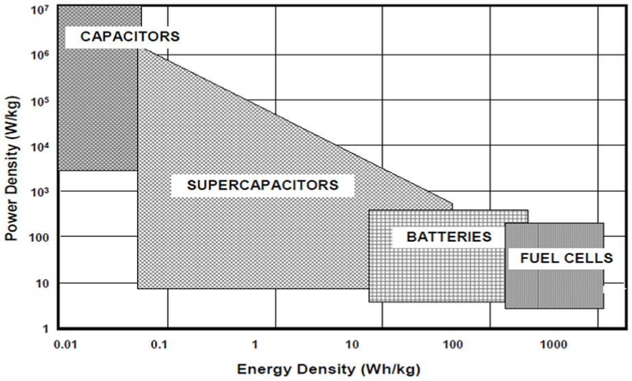
Ragone plot of energy storage devices.
Apart from this storage application, SC can be used as a measuring device for performing V–I characterization of solar cell/module significantly.
They have the following characteristics:
(a) Desirable control of the plotting time after the voltage of SC approaches VOC;
(b) Thermal management of the SC bank is possible without the use of any kind of heat sink, as heat dissipation is not expected to cross the level of a few watts, which prevails for only 5 to 10 s;
(c) A high coulombic efficiency exceeding 99%;
(d) An adequate range of capacities of SCs is commercially available with low ESR values (within a few milliohms) 26 —a feature measuring at appropriate as a loading element to the PV module;
(e) A wide voltage range of SCs is available, compatible with the open circuit voltages of standard PV modules and panels;
(f) With the use of SC as the load, plotting time has been estimated theoretically, and such estimates have also been practically validated. 10
Moreover, an experimental estimation of heat dissipation for 100.0 Wp PV modules using SCs is shown in Table 1. The heat dissipation values in the last column have been estimated by considering the individual ESR value of the SCs to be 0.02 Ω, and the total ESR value of the SC bank is 0.12 Ω (optimum combination of six SCs in series). Same experiments were also carried out using capacitances of rating of 10,000 µF, 25 V with 1 Ω ESR value, and the charging currents utilized to estimate the different heat dissipation amounts as shown in Table 2.
Heat dissipation of 100 Wp PV modules using SC loading.
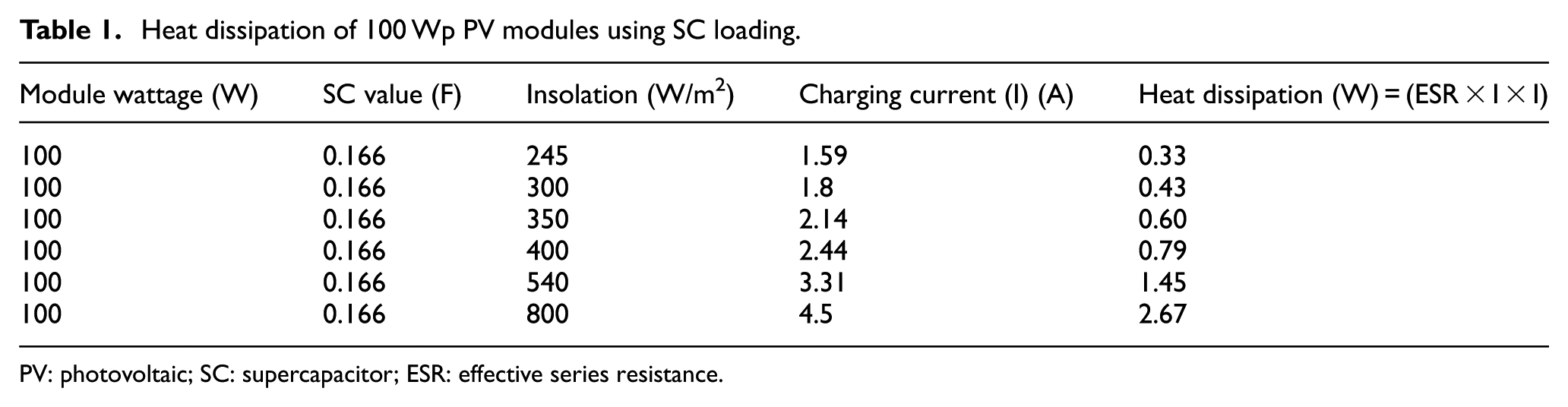
PV: photovoltaic; SC: supercapacitor; ESR: effective series resistance.
Heat dissipation 100 Wp PV modules using capacitor loading.
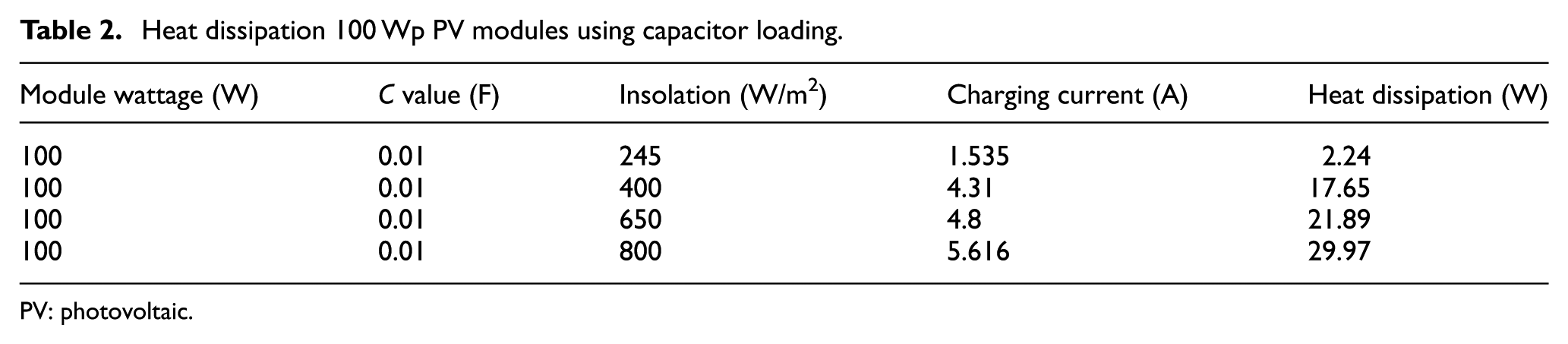
PV: photovoltaic.
The further disadvantage of using the capacitor as the load to the PV generator leads to a bulky I–V plotter, which also makes capacitor-based plotters inconvenient for transportation.
The estimate of heat dissipation which is totally resistive is shown in the last column of Table 2, assuming the ESR value of the standard capacitor to be 1 Ω. Choosing standard capacitances of lower ESR value will lead to exorbitant price of capacitors.
The next subsection points to the I–V curve tracing time estimates obtained using SCs as the load.
Curve tracing time of PV characterization
Curve tracing time is an important factor while measuring the electrical parameters of a PV module. If it is too fast, some of the points on the I–V curve may be missed, leading to improper estimates of maximum power point (PM). A very long curve tracing time is likely to cause pronounced and adverse thermal effects on any PV device.
Thus, the proper selection of SC banks with low ESR values was necessary to keep the plotting time within a few seconds. Here, authors have dealt with separating the I–V characteristics into two linear pieces as shown in Figure 2. This means that an I–V curve contains the following segments:
One extending from (0, ISC) to (VM, IM);
Second segment extending from (VM, IM) to (VOC, 0).
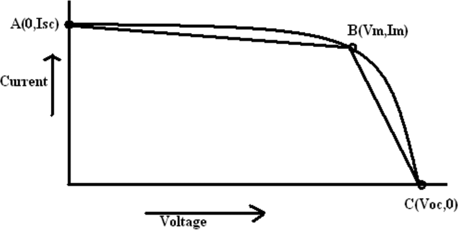
Piecewise linear break-up of the V–I characteristics of a PV generator.
For the analysis, the PV curve ABC is considered in two linear parts
The developed equation for curve tracing time is shown below
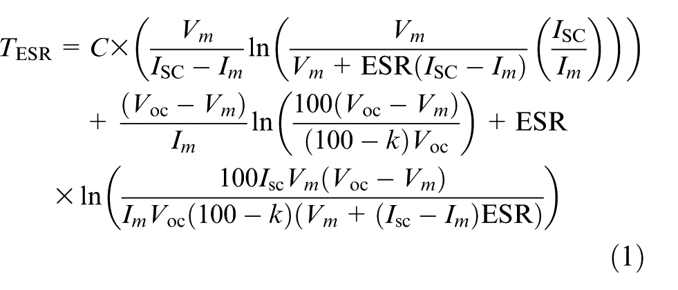
where TESR is the curve tracing time considering ESR, as in equation (1), and ESR is the effective series resistance of SC, where the other symbols have usual meanings that pertain to PV modules.
The detailed steps are worked out in an earlier publication 10 of the authors. In another work 17 for analyzing the curve tracing time using the capacitive load, the time was estimated as follows
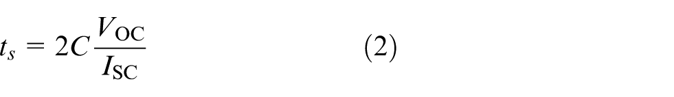
Equation (1) depicts a clear dependence of plotting time on VOC, ISC, VM, and IM of PV modules along with the ESR and supercapacitance value C of the chosen SCs. In contrast, the time taken with the capacitive loading is given by equation (2), showing its dependence on two electrical parameters of the PV module only.
The time taken for curve tracing using SC-based loading as given in equation (1) is shown in Table 3. This table shows the variation of the plotting time between 5 and 8 s depending on the various values of the SC banks and the corresponding ESR of the configuration.
Curve tracing time (theoretical and experimental) for different SC values at 900 W/m2 insolation for 100 Wp PV module.
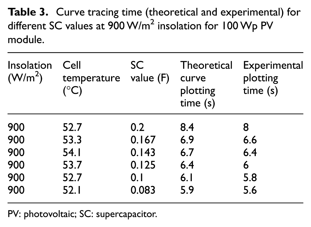
PV: photovoltaic; SC: supercapacitor.
The four electrical parameters (ISC, VOC, IM, and VM) in a PV characteristic are essential for faithful reproduction of the I–V curve trace. Such a correlation is shown in equation (1) which includes another significant parameter, the ESR value of SC, in the curve tracing time.
Standard capacitors used for the purpose possess higher values of ESR in the range of 1 Ω, and use of such capacitors will lead to considerable heat loss as indicated in Table 2. On the contrary, procurement of capacitors with lower values of ESR is a much costlier proposition.
Configuration of SC bank
The task of choosing the elements of the SC bank was performed with initial priority on low ESR values to keep the curve tracing time within a few seconds:
(a) In the first phase, 10–100 Wp PV module sizes were considered. Six numbers of series-connected 1 F, 5.5 V SCs were chosen since the VOC of the 10–100 W PV modules lies between 21 and 25 V, respectively. For the first case, six numbers of KAMCAP SCs have been used with low ESR (0.02 Ω) values. This resulted in an equivalent capacitance of the SC bank = 1/6 = 0.166 F.
(b) In the second phase, 320 Wp PV modules were the device under test. Here, the SCs with the lowest ESR values were found, having the specifications of 7 F, 5.5 V. Since the VOC of a 320-Wp module (the largest capacity building block in Indian PV arrays) is 48 V, a series connection of nine identical SCs was required, resulting in an equivalent capacitance of 7/9 = 0.77 F.
Measurement system description
Figure 3 represents typically the block diagram of the I–V tracer developed in this work.
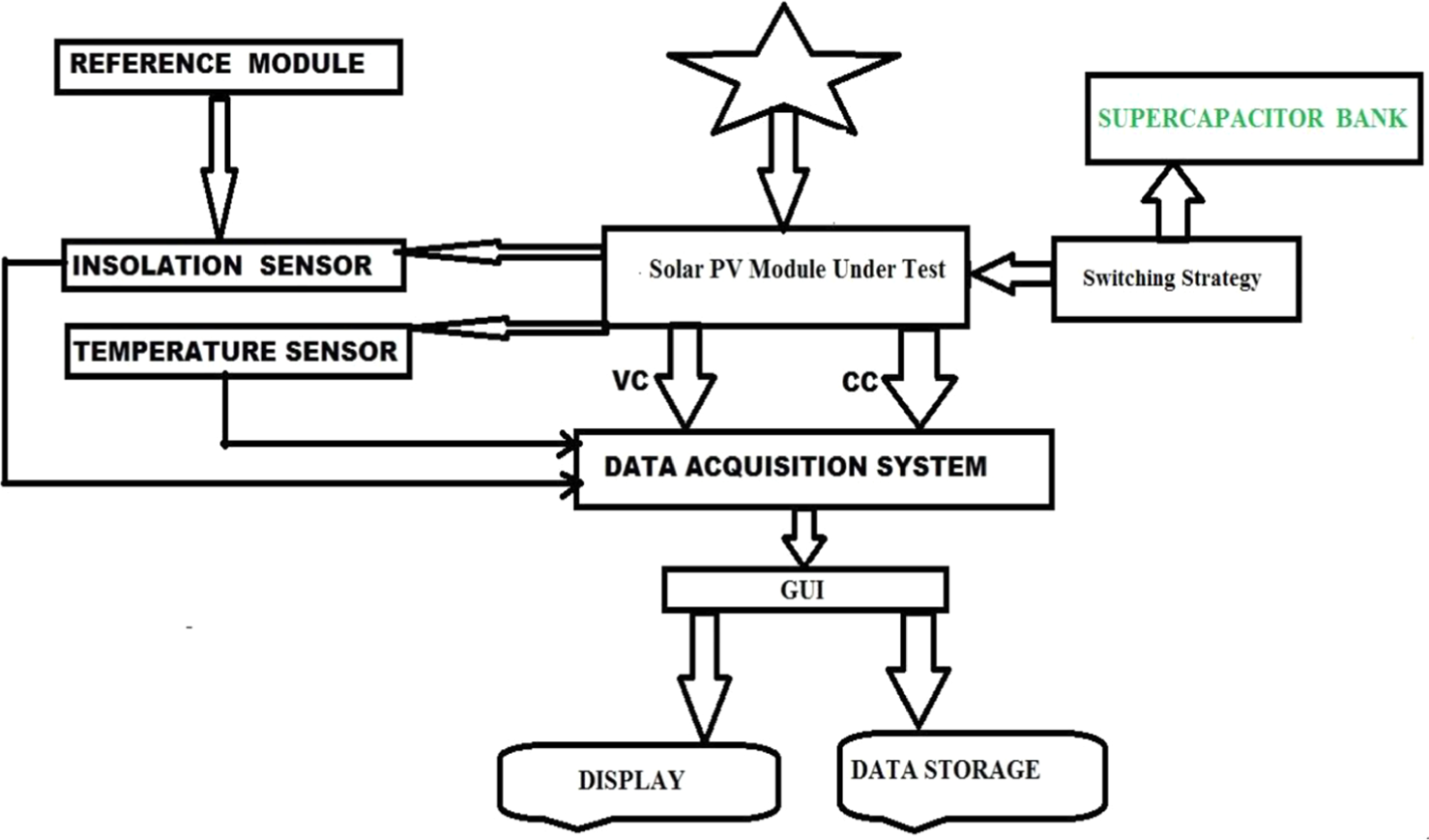
Block diagram for I–V tracer for PV characterization.
The process flowchart shown in Figure 4 indicates the sequences of operations necessary for completing the measurement procedure. 27
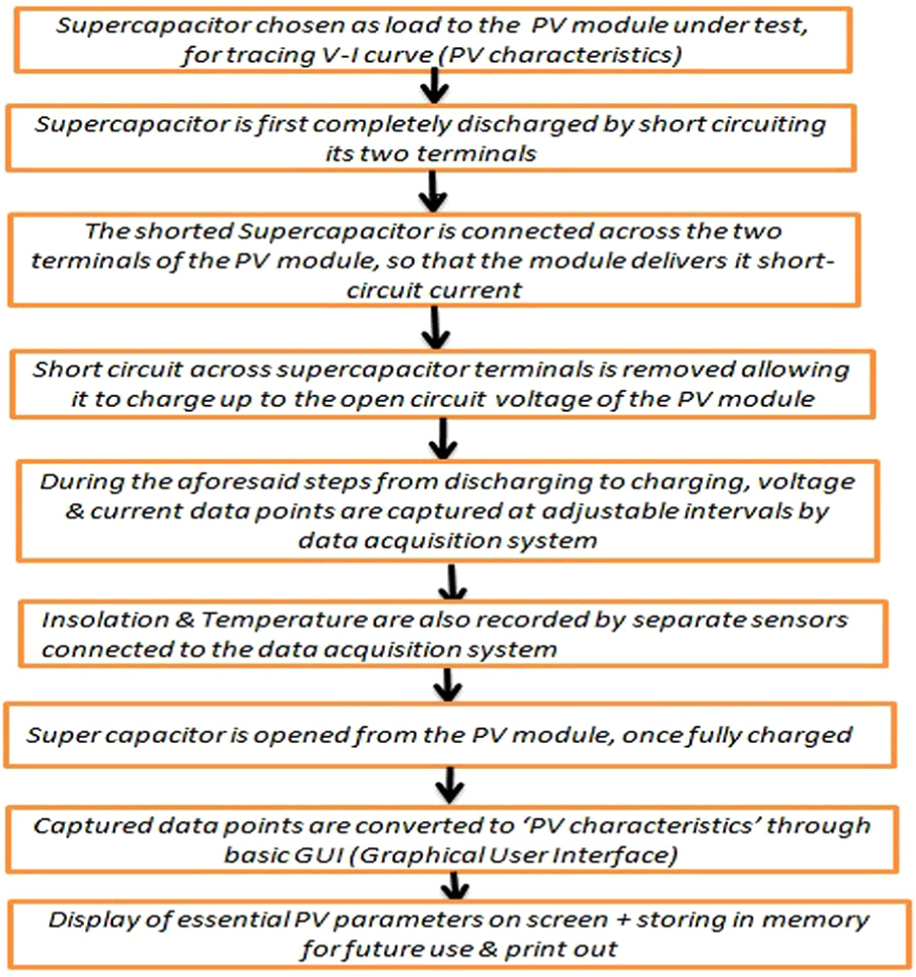
Process flowchart of I–V tracer for PV characterization. 27
The ACS 712 IC used here is a “Hall Effect”–based linear current sensor. For the PV module back-surface temperature measurement, an LM35DT-type temperature sensor has been used. The PIC 18F46K22 microcontroller is the base of the embedded system which manages the SC control or rather its switching strategy and different data acquisitions, and executes the program necessary for display on the GLCD (graphical liquid crystal display) screen. The sequence of operation is shown in the flowchart (Figure 4) of the algorithm for appropriate data acquisition and control. The GLCD with 240 × 128 pixels and screen size of 4.7 in is integrated with the T696 processor. The actual circuit of the whole I–V tracer setup is shown in Figure 5(a), and the microcontroller unit is shown in Figure 5(b).
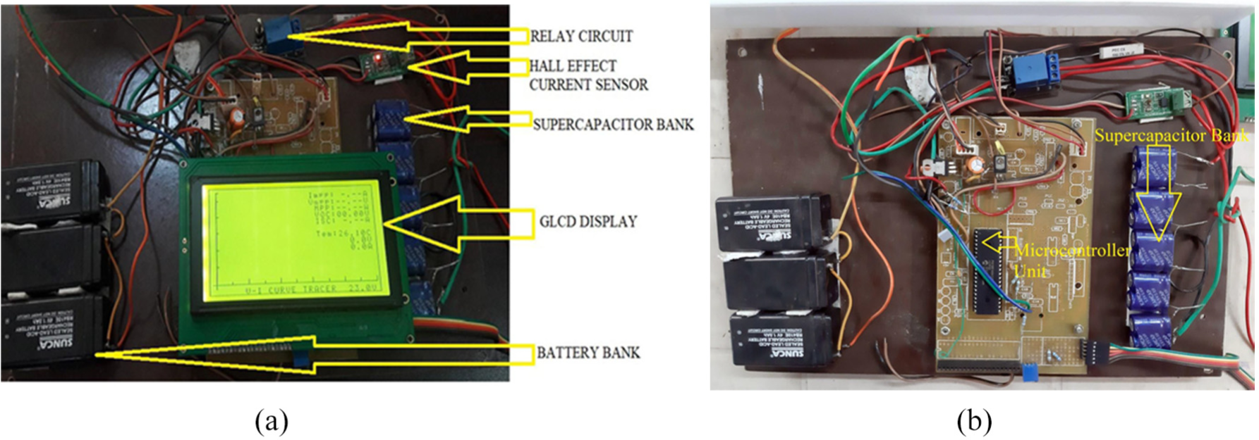
(a) Electronic components in V–I measurement setup and (b) microcontroller unit of the developed I–V plotter which is obscured behind the GLCD display unit.
Cost estimation for the developed I–V plotter
The cost of the various components which constitute the I–V tracer is listed in Table 4. However, the cost of manpower is not included in the estimation.
Cost estimation for the IIEST I–V plotter.
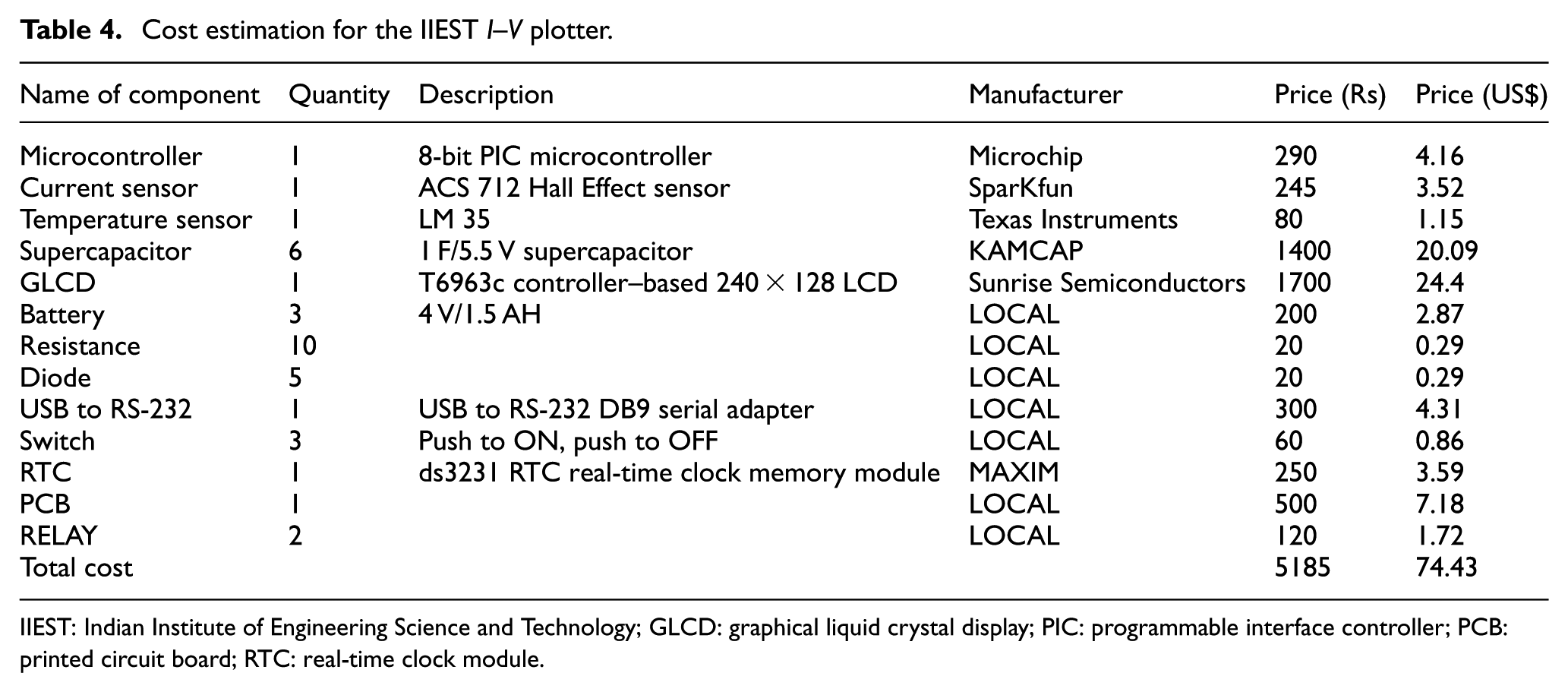
IIEST: Indian Institute of Engineering Science and Technology; GLCD: graphical liquid crystal display; PIC: programmable interface controller; PCB: printed circuit board; RTC: real-time clock module.
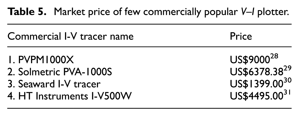
In case of industry-available I–V tracer, the cost is in the range of US$500–US$9000. 28 Table 5 shows the current market price of commercially available I–V tracers.
Market price of few commercially popular V–I plotter.
Results and discussion
Currently, in India, the local PV market is dominated by assorted poly-Si PV modules. According to the current PV scenario in India, Vikram Solar Ltd. (VSL) is one of the foremost PV manufacturing companies. Modules manufactured by the aforesaid company have been used in this study.
A series of experiments were conducted using different capacities of poly-Si modules under varying levels of insolation and ambient temperature. A comparison between IIEST tracer and commercial tracer is shown in Figure 6(a) and (b). The first curve (Figure 6(a)) is captured by the commercial curve tracer (PVPM1000X) which is used by VSL, whereas the next curve (Figure 6(b)) is captured using the developed IIEST I-V tracer.
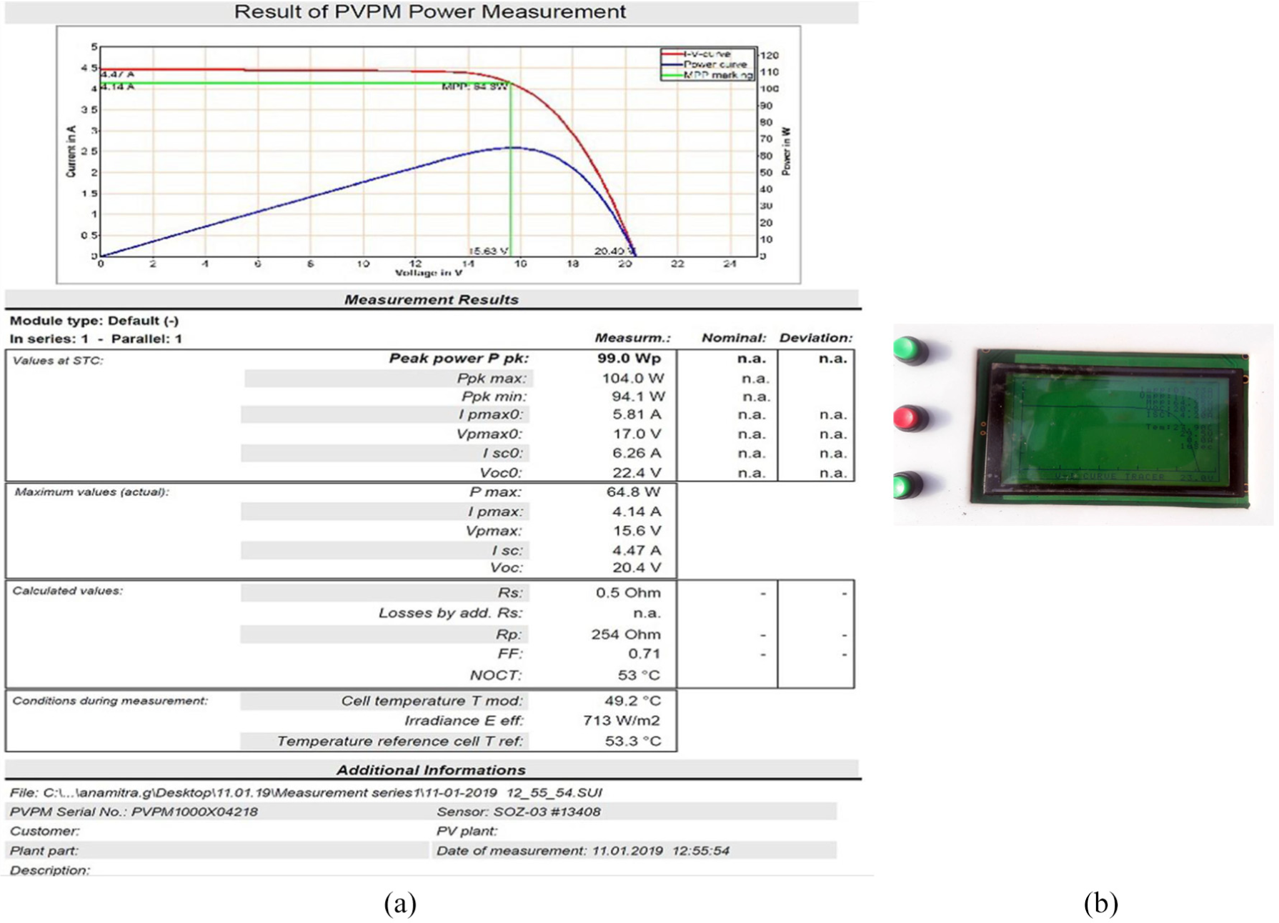
(a) V–I curve captured using PVPM1000X for 100 Wp PV module and (b) V–I curve captured using IIEST tracer for 100 Wp PV module at insolation of 713 W/m2.
Tables 6 and 7 display the PV parameters captured simultaneously by the developed curve tracer (IIEST I-V) and the curve tracer (PVPM1000X), respectively.
IIEST curve tracer data of 100 Wp poly-Si test (11 January 2019).
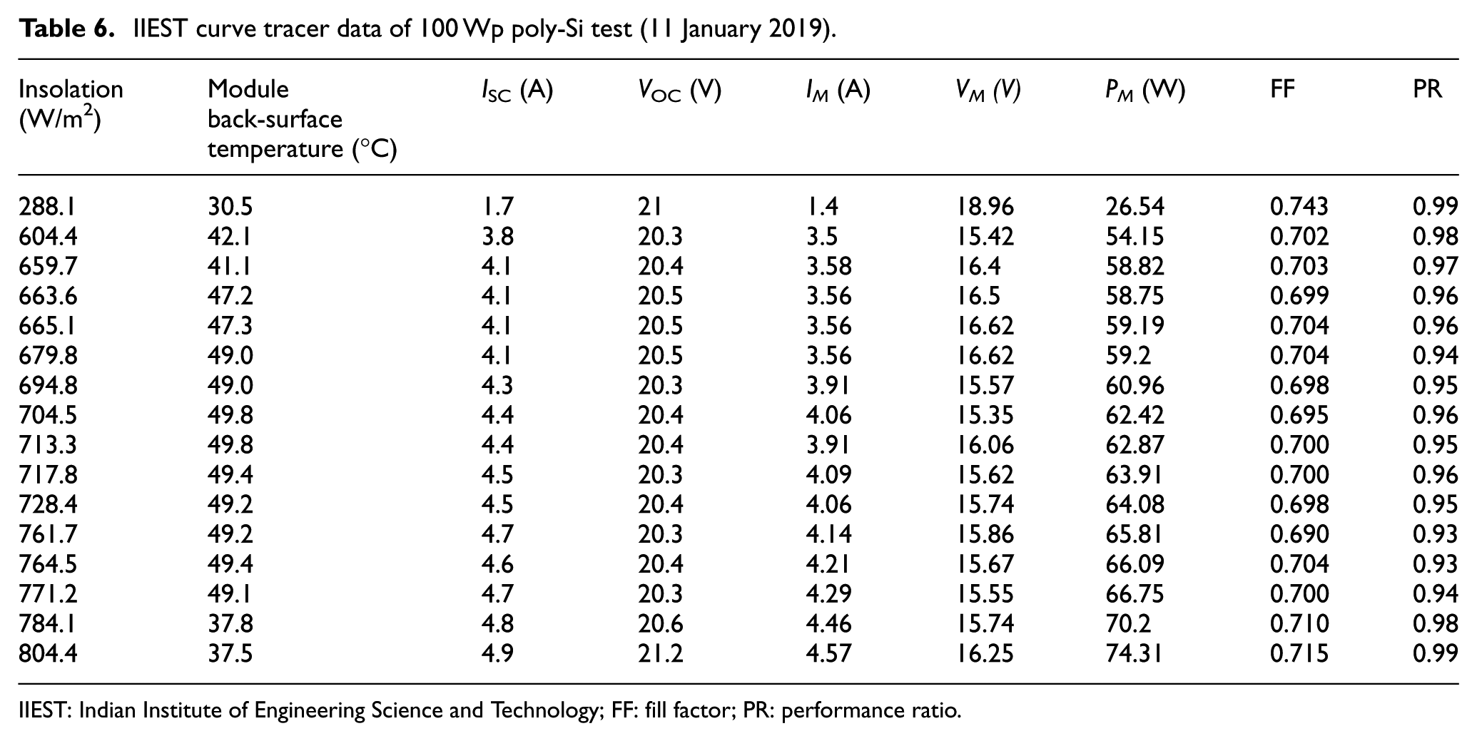
IIEST: Indian Institute of Engineering Science and Technology; FF: fill factor; PR: performance ratio.
PVPM1000X curve tracer data of 100 Wp poly-Si test (11 January 2019).
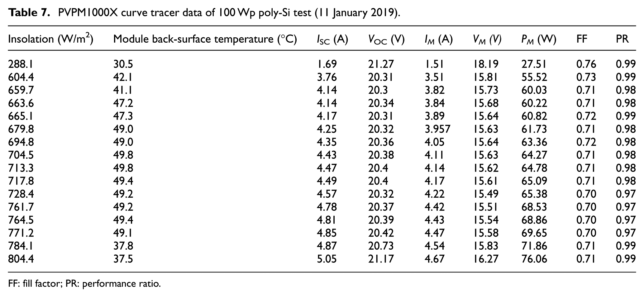
FF: fill factor; PR: performance ratio.
From the above tables, it is clearly seen that the fill factor (FF) range using the curve tracer from IIEST is 0.695–0.74, whereas the FF range using PVE1000X is 0.7–0.76. In the case of performance ratio (PR) variation, 32 the range for IIEST tracer is 0.93–0.99 and for PVPM1000X is 0.97–0.99.
The maximum power point deviation recorded by the developed curve tracer and the industry standard PVPM1000X is shown in Table 8, which is within the limits of 2%–4%.
Maximum power point deviation for 100 Wp poly-Si PV module.
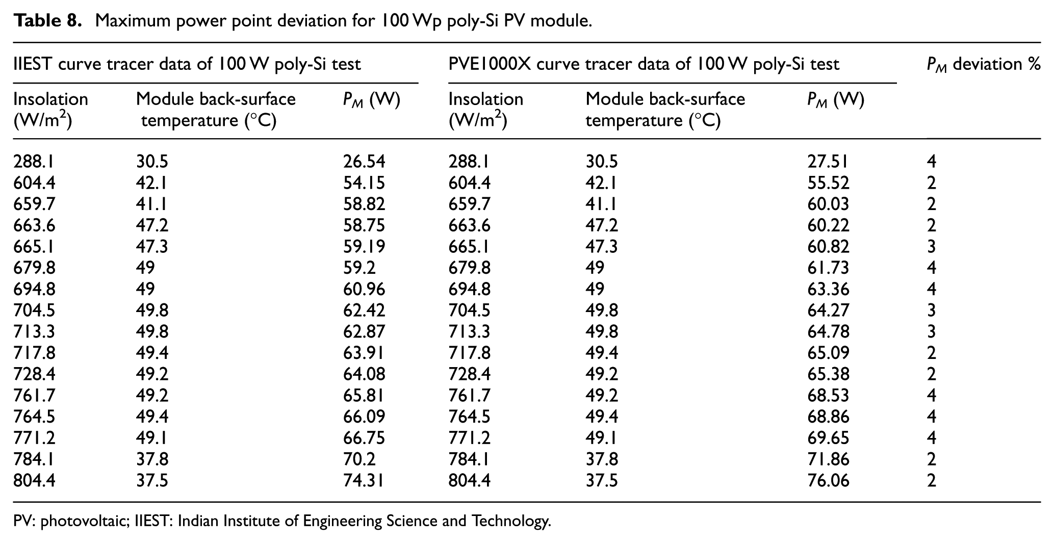
PV: photovoltaic; IIEST: Indian Institute of Engineering Science and Technology.
In order to confirm the accuracy of the newly developed I–V tracer, a few comparative measurements with YOKOGAWA Power meter were done for validation of the new metrological procedure; these are shown in Figure 7(a) and (b), respectively.
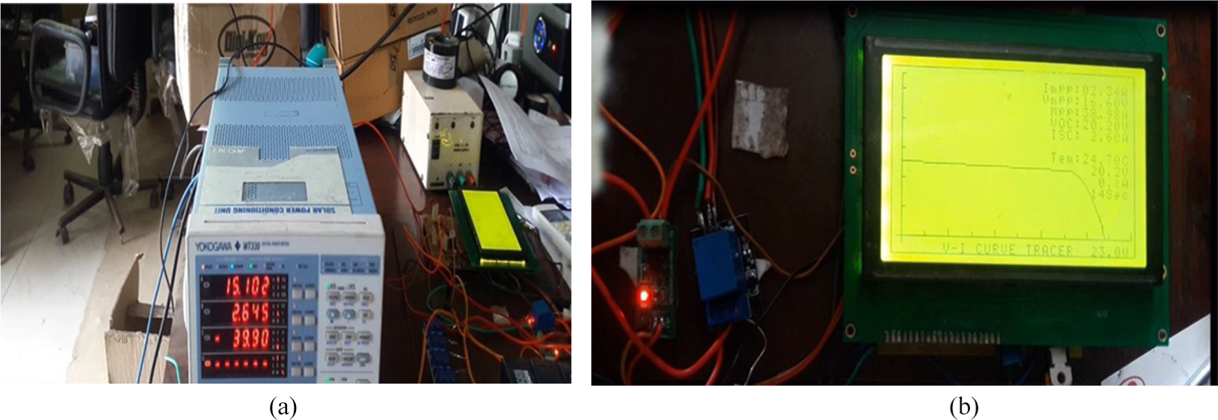
(a) YOKOGAWA power meter peak power reading of 100 Wp PV module at insolation of 419 W/m2 and (b) IIEST tracer peak reading of 100 Wp PV module at insolation of 419 W/m2.
The regression analysis 33 of the three principal electrical parameters (ISC, IM, PM) was estimated on the 100-Wp PV module for various levels of insolations and is depicted in Figures 8–10, respectively.
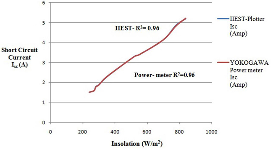
Regression analysis of ISC against insolation variation.
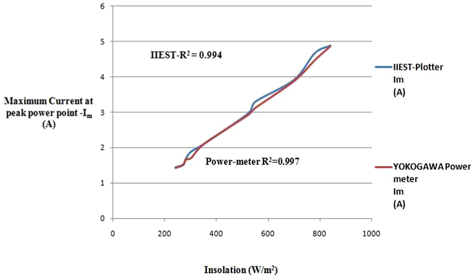
Regression analysis of IM against insolation variation.
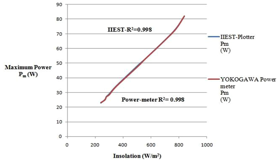
Regression analysis of PM against insolation variation.
The readings from the developed tracer fall within 1%–2% of YOKOGAWA
34
measurements, which is known to exhibit a
The final prototype of the I–V tracer system is shown in Figure 11.
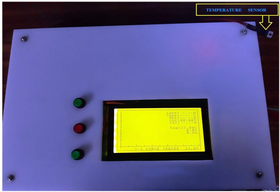
IIEST V–I tracer.
With reference to Figure 12(a) and (b) shown below, the variation of FF and PR with respect to insolation in the months of December, March, and July is indicated. Since the variation of FF takes place in a range of 0.7–0.8 and the PR from 0.8 to 0.95, it can be deduced that measurements carried out by the developed method highlight the reproducibility of the proposed system. Similar elaborate experimental observations have been carried out with poly-Si PV modules of varying capacity. This effort 35 has been published elsewhere.
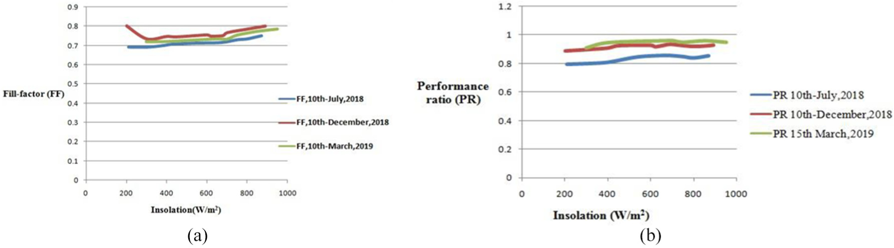
(a) FF versus insolation graph of 100 Wp PV module for three different seasons and (b) PR versus insolation graph of 100 Wp PV module for three different seasons.
Design challenges
(a) To capture ISC accurately: precise care is to be taken to store the first recording of the initial current point (ISC) after the relay contact is closed for shorting the SC terminals.
(b) Appropriate current measurement: since the developed curve tracer specifies a range (0.5–6.2 A), choice of accurate Hall Effect sensor is essential.
(c) Optimizing the sampling rate: keeping in view that the memory space is limited (RAM) for the microcontroller-based I–V plotter. If enough I–V data points are not stored, then the quality of the I–V characteristics gets affected.
(d) Accurate peak power measurement: a set of rigorous trial and error method has been exercised to fix up a suitable sampling rate for capturing the precise value of the maximum power point (PM).
(e) Selection of GLCD: the GLCD should have high resolution and be easily programmable. Since the I–V plotter is designed for field applications and preferably outdoor testing, monochrome GLCD is chosen.
Conclusion
A novel measurement technique for recording the I–V characteristics of any PV module has been put into practice for the first time at IIEST, Shibpur, India. The device so developed incorporates SCs as the loading element in lieu of resistances, capacitances, or electronic loads.
The major attractive features of this new type of plotting device are the following:
(a) The use of SCs as loading permits the realization of lightweight and low-cost (Tables 4 and 5) I–V plotter, eliminating the need for heat sinks (Tables 1 and 2).
(b) The values of FF for the IIEST curve plotter lie within a range of 0.70–0.74, closely in tune with the measurements from the PVPM1000X commercial plotter, covering a range of 0.70–0.76 (Tables 6 and 7).
(c) With reference to the same tables, the range of PR is within the limit of 0.92–0.99, which is exactly similar to the range indicated by the PVPM1000X plotter (Tables 6–8).
(d) Measurement of peak power has been emphasized through an additional check with YOKOGAWA power meter, indicating excellent agreement of regression coefficient (R2) values for the chosen parameters (Figures 8–10).
(e) Elaborate measurements of I–V characteristics have been carried out on three specific dates, which typically represents three different seasons. Here, the reproducibility of the measurement technique is clearly advocated through Figure 12(a) and (b) in “Results and discussion” section.
Further research work is in progress in collaboration with PV manufacturers for realizing a scaled-up version of the I–V plotter so that the upcoming PV industries can utilize the same version fruitfully.
Footnotes
Acknowledgements
The authors wish to thank the Centre of Excellence in Green Energy and Sensor Systems, IIEST, Shibpur, India, for helping in the entire testing procedure with different instruments. Also, it needs to be noted that without the cooperation of the management and engineering team of Vikram Solar Industries, the viability of field trials on actual factory premises could never have been conducted. The authors are indebted to Dr Nikhil Agrawal, lead—new product development, R&D, and appreciate the diligence of Mr Supratik Ghosh and Mr Mohan Kumar of this company for helping in taking the measurements and enabling them to validate the data with the reference test setup.
Declaration of conflicting interests
The author(s) declared no potential conflicts of interest with respect to the research, authorship, and/or publication of this article.
Funding
The author(s) received no financial support for the research, authorship, and/or publication of this article.