
Abstract
Low-power design for test is the need of the hour for any system-on-chip designer. The low-power design techniques have been a major challenge to both the designer as well as the testing engineer. With so many advancements in low-power technology in the phase of register transfer logic design, functional verification, register transfer logic and physical synthesis and physical design. Design for test is not an exception to this. The low-power design-for-test techniques can be applied at various levels of the design-for-test flow as in the scan insertion stage, automatic test pattern generation simulations stage, testing stage, and so on. Some of the reasons for the high-power utilization in the design-for-test phase can be due to the external circuitry being inserted during the design phase and not used in the functional mode. The complete circuit will be active in the test mode only. In this paper, the focus will be primarily on reducing the power during the automatic test pattern generation scan synthesis phase. All the scan flops are connected by a common scan clock with a fixed frequency. The intention of this study is to divide the clock frequency by half and make sure that the power is reduced without affecting any timing violations. Since the scan clock frequency is low, it can be further divided to ensure that power is reduced without affecting the testing process of the chip.
Keywords
Introduction
As the technology is shrinking, more and more power challenges are on the rise. Handling the power issues in the lower technology nodes has become more complex and challenging for the application-specific integrated circuit (ASIC) designers. Complex systems on chip (SoCs) require huge data to test them, thereby increasing the time for testing and the tester memory. Low-power design techniques are needed both at the functional mode as well as at the test mode of the design.1,2 As the complexity of the integrated circuits (ICs) and the feature size continues to reduce, the power consumption becomes one of the key issues not only at the functional level but also at the manufacturing level. The functional operation with higher power consumption implies the following:
(a) High design cost and high manufacturing cost;
(b) High system cost because of the requirements of packaging and cooling;
(c) Short device life cycle in addition to less device reliability;
(d) Inadequate battery life for portable applications.
Hence, it becomes important that the power is saved in parts of the chip that are not used always.3,4 All the SoCs integrate multiple intellectual properties (IPs). Every IP has got its own power requirements and specifications. When multiple IPs are integrated in a single SoC, there is every chance that the total power of the chip might shoot up. This will lead to overall failure of the power management system of the chip. To overcome such problems related to power saving, each of the IPs can be moved among the power modes like power-off, power-on, or sleep. Every IP on SoC can be divided as power domains and these domains can be turned on and off in accordance with the power mode.5–7
Low-power design for test (DFT) has always been a challenge to the DFT engineers. One reason is that a lot of additional circuitry is added during the test phase and one has to ensure that the switching activities during this phase are under control. This phase primarily has two aspects: (1) scan synthesis and (2) automatic test pattern generation (ATPG) simulations phase. Most of the techniques that are applied to reduce power in the DFT phase are as follows:
(a) Clock gating the scan cell;
(b) Special clustering and ordering of the scan cells improves the effectiveness of power reduction techniques based on test planning and test generation;
(c) Partitioning techniques are used to reduce the power.
This idea of dividing the scan clock is novel because the scan clock is used only to test the test mode of the chip and not the functional mode. Usually, the scan clock has a much lower frequency than the functional clock. However, the scan clock is not always on which enables the clock gating technique to effectively shut down the scan clock when it is not in use. In this approach, the authors have used the method of clock reduction (decreasing the scan clock frequency by half) within the permissible range of the specifications for achieving the low power in the circuit. The main advantage of reducing the scan clock frequency compared to the other methods of low power is that the power is reduced to half (power is directly proportional to frequency) and also fixing the timing violations is considered in this approach. In this novel approach, the authors have implemented the low-power DFT technique during the scan synthesis phase using the clock reduction technique with minimum timing violations. During the ATPG phase, there are techniques to minimize the power using unified power format/common power format (UPF/CPF) flows. However, the idea to minimize power at the scan design phase is a novelty in this paper.
DFT flow diagram
A typical ASIC design flow till the DFT phase is as shown in Figure 1.
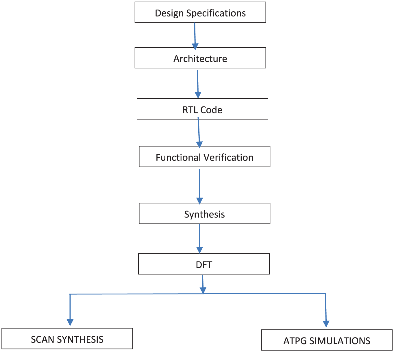
DFT flow diagram.
From the ASIC design flow in Figure 1, the DFT phase starts after the completion of synthesis and generation of the synthesized netlist.8–10 As it is evident from the flow diagram, the low-power DFT technique can be applied in two phases of the DFT flow:
Scan synthesis phase;
ATPG simulations phase.
Scan synthesis phase
As shown in Figure 2, during the scan synthesis phase, the following steps take place:
(a) Scan configuration;
(b) Scan replacement;
(c) Scan reordering;
(d) Scan stitching.
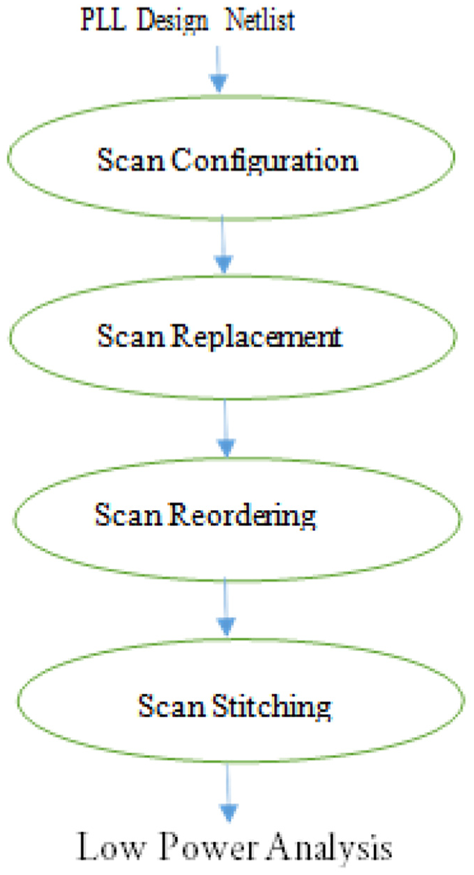
Scan synthesis flow chart.
During the ATPG simulations phase, the following steps take place:
(a) Read synthesis netlist from design;
(b) Read ATPG library files, test procedure files, and do files;
(c) Build the ATPG model;
(d) ATPG DRC checking;
(e) Generate fault list;
(f) Generate test vectors;
(g) Validate test patterns using simulations.
Low-power specification formats
The two common formats used in the industry for power savings are as follows:
UPF;
CPF.
While UPF design flow is implemented with the help of Synopsys electronic design automation tools and tested on Synopsys generic 90 nm and 32/28 nm libraries, CPF design flow was designed by Cadence Design Systems and then contributed to Si2. UPF has been driven mainly by Synopsys, Mentor Graphics, and Magma. There is very subtle difference between the two flows. Most of the companies follow both the flows. Either of these flows is used to reduce power consumption at various levels of the ASIC design flow. 12
Low-power DFT techniques
Some of the commonly used low-power techniques in DFT are as follows. All the below-mentioned techniques are already implemented in the DFT domain. The clock reduction method is novel as it is done at the scan synthesis phase and the timing violations arising due to this clock reduction are also considered to be fixed. The power is reduced by nearly 50% and no functionality or performance of the chip is affected.
Clock gating circuitry
It is a technique used for the reduction of power consumption in the power-on domain by blocking the clock dynamically before reaching a set of flip-flops or latches. It is like switching off the clock when it is not being used functionally. Since continuous switching consumes a lot of dynamic power, this technique helps save power when the clock is not being used. 13
Power domains
Separating the whole design into different power domains will ensure that each of the blocks can be powered down or powered up individually by controlling the power switches utilized for gating the power supply connection to every power domain block. 14
Low-power cell
While testing the design, the capacity of the state preservation registers to keep hold of their state needs to be verified when the power domain is powered off. Isolation cells are located at the limit of two power domains keeping in mind to isolate the power-on and power-off domains.
Multiple supply voltages
Based upon the operating conditions, different power domain blocks are subject to different supply voltages and each power domain block is connected to other power domain block with the help of level shifters.
Power-aware DFT
Once the scan synthesis starts, the functional flops are replaced by their scan equivalent flops. During the scan stitching process, the power-aware DFT is applied by the respective power domain after the partitioning of scan chains under the condition that there are adequate scan I/Os in every power domain and they can have their dedicated scan I/Os, control signals, and test clocks. This guarantees that every power domain is having dedicated scan chains which are active in the power domain that is ON.15,16
Power switches
In order to minimize power dissipation, particularly leakage power dissipation caused by the shrinking power technologies, power switches are generally employed in modern low-power design circuits. One or more power switches are equipped at different parts of the design to facilitate the functionality of power gating.
Implementation of the low-power DFT technique
In the current implementation in this paper, for the low-power DFT, we have adjusted the frequency of the scan clock in such a way that it meets the design specification and also directly resulted in reducing the power consumption in the circuit.
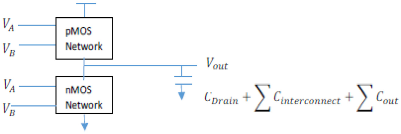
The input design is a phase-locked loop (PLL) with multiple clocks. A simple PLL design looks as shown in Figure 3.
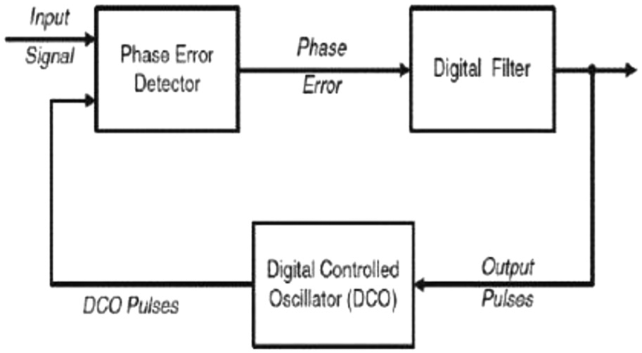
PLL block diagram.
PLL is a circuit that can be used for high-frequency application and very short interlocking time. PLL is a feedback system that detects the phase error and then adjusts the phase of the output. The phase error detector detects phase error between the output and the input through the feedback system. The digital controlled oscillator (DCO) adjusts the phase difference. One of the primary applications of PLL is in carrier synchronization and bit synchronization systems to improve their synchronization properties. Another important application of PLL is its use as a frequency synthesizer. Digital phase-locked loop (DPLL) can be classified into two major categories: (1) uniform sampling DPLLs and (2) non-uniform sampling DPLLs.
The gate-level netlist is taken as the input for performing the DFT process and implementing the low-power DFT technique of decreasing the scan clock frequency and dividing it into multiple power domains. Here the emphasis is on reducing the dynamic power.
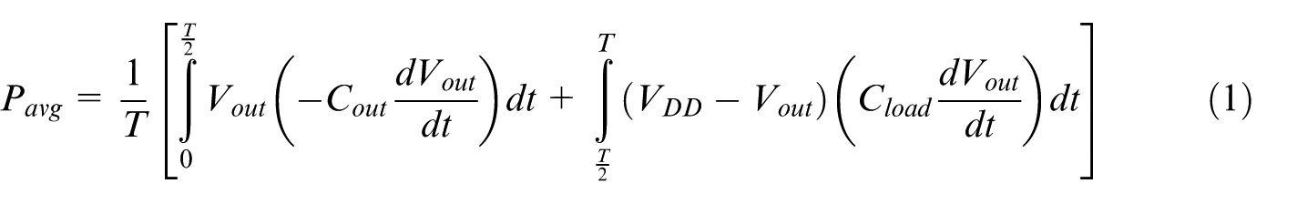
The general representation of CMOS (complementary metal-oxide semiconductor) logic gate for switching power calculation is shown in Figure 4
CMOS logic circuit for power calculation.
The average power consumption can be expressed as
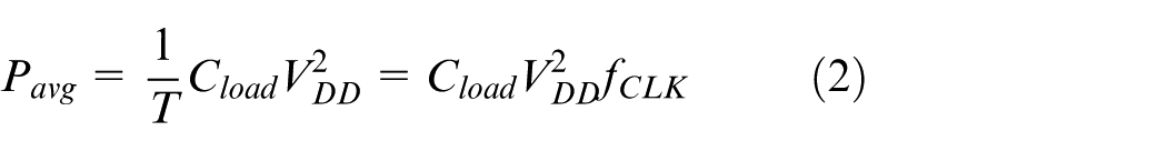
The transition rate of the nodes can be slower than the clock rate. For better representation of this behavior, a node transition factor (α′) must be introduced

The generalized expression for the average power dissipation can be rewritten as
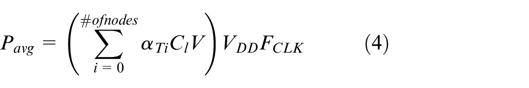
As we can see from equation (4), power is directly proportional to the clock frequency. Hence, reducing the clock frequency such that it falls between the specification ranges, the power can be reduced without affecting the timing violations.
Results of the low-power DFT technique on PLL netlist
The results of this experiment at the scan synthesis level after varying the clock frequency are tabulated in Table 1.
Comparison table showing the power values before and after applying LPT for PLL.
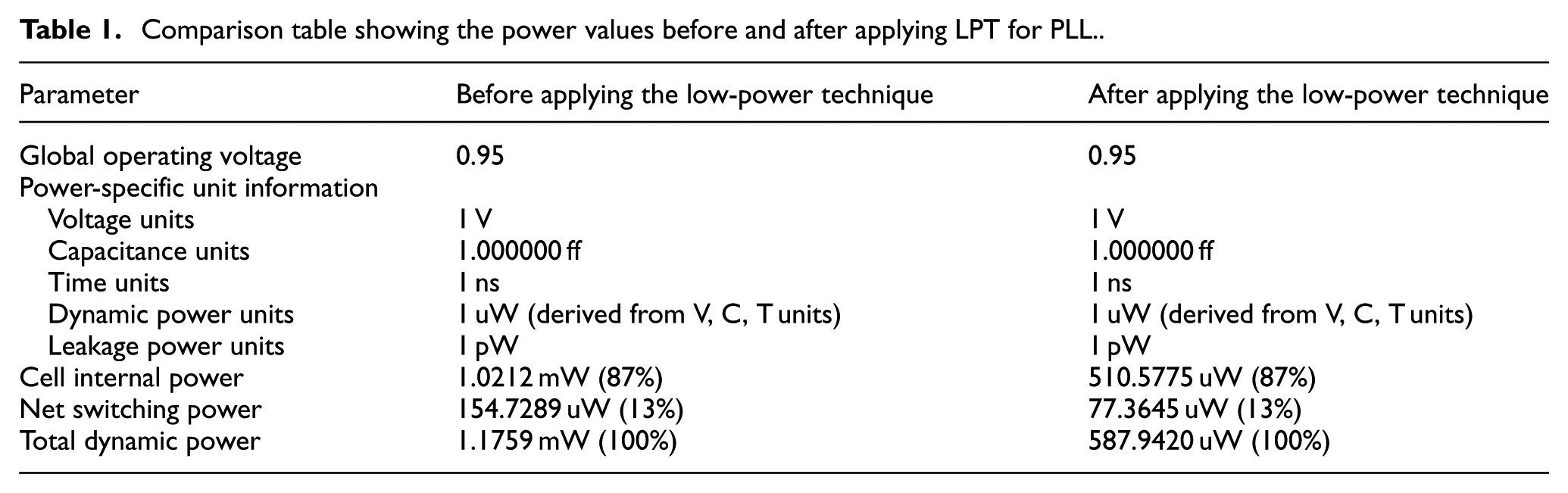
As can be seen from Table 1, it is evident that the power has reduced by approximately 50%. These results have been obtained for the PLL design netlist.
Table 1 explains the results of the application of the low-power DFT technique on PLL netlist using the Synopsys Design Compiler tool from Synopsys. The above results have been generated with the help of the Synopsys DC tool. It is observed from Table 1 that the parameters like cell internal power, net switching power, and total dynamic power have nearly 50% reduction after applying this technique.
Cell internal power is the power dissipated within the boundary of a cell. During switching, a circuit dissipates the internal power by charging or discharging of any existing capacitances internal to the cell.
Net switching power occurs when signals which go through the CMOS circuits change their logic state. At this moment, energy is drawn from the power supply to charge up the output node capacitance.
Total dynamic power can be obtained from the following equation
All the above parameters have been reported by the Synopsys Design Compiler using the command report_power.
Synopsys DC is a synthesis tool that takes the design netlist as the input and reports the area, power, and so on consumed by the chip. There are no simulations carried out by the authors as they are not considering the functionality of the PLL netlist or the asynchronous first-in first-out (FIFO) netlist used. They are only taking the netlist as the input and carrying out the low-power DFT technique research on the inputs provided by the designer. Hence, there are no simulation reports shown in the results.
Results of the low-power DFT technique on the asynchronous FIFO design netlist
The results of this experiment at the scan synthesis level after varying the clock frequency are tabulated in Table 2.
Comparison table showing the power values before and after applying the low-power technique for asynchronous FIFO.
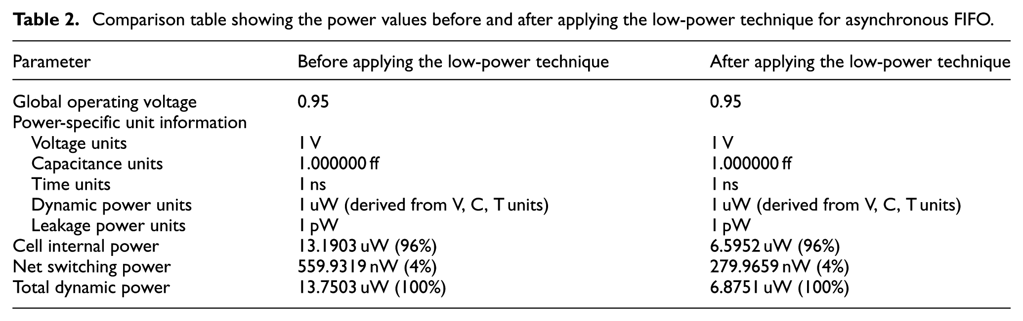
As can be seen from Table 2, it is evident that the power has reduced by approximately 50% by applying the low-power DFT technique used in this paper. These results have been obtained for the asynchronous FIFO design netlist.
By reducing the clock frequency by half, the power has also reduced by 50% which is compliant to equation (2). This is the reduction technique for dynamic power which is also the switching power in any SoC.
From Figures 5 and 6, we can observe the decrease in power after applying the low-power technique in DFT methodology as discussed in section “Implementation of the low-power DFT technique.”
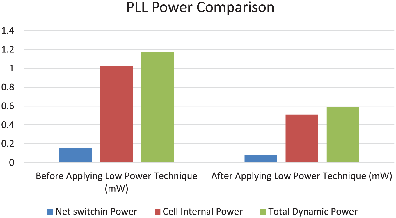
PLL graphical representation of power comparison.
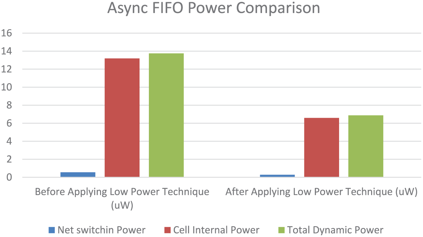
Asynchronous FIFO graphical representation of power comparison.
Conclusion
As we can see from the above results on two different design netlists, when the clock frequency is reduced from 50 to 25 MHz, the power is also reduced by nearly 50%. All these results have been calibrated by ensuring that there are no setup or hold violations in the circuit after varying the clock frequency. It is clearly proved from equation (3) that power is directly proportional to frequency. One of the techniques which will be applied in the further version of the paper will be dividing the scan clock for even and odd chains and thereby reducing the power consumption in the scan chain.
Reducing the scan clock frequency does not affect either the functionality or the performance of the IC. The scan clock frequency is used only for the purpose of DFT and it is not going to be used as the functional clock. When the DFT mode is enabled, the scan enable is set to logic “1” and no functional paths are affected. Hence, any change in the scan clock frequency will not affect either the functionality or the performance of the IC.
Footnotes
Acknowledgements
I personally would like to thank my guide Dr Hari Kishore Kakarla for his support in implementing this low-power DFT scheme. I would also like to thank the management of K L University for giving me this opportunity to conduct the experiment and using their lab premises.
Declaration of conflicting interests
The author(s) declared no potential conflicts of interest with respect to the research, authorship, and/or publication of this article.
Funding
The author(s) received no financial support for the research, authorship, and/or publication of this article.