
Abstract
Background:
In this study, a machine vision–based method was developed for automated in-process light-emitting diode chip mounting lines with position uncertainty. In order to place the tiny light-emitting diode chips on the pattern of a printed circuit board, a highly accurate mounting process is achieved with online feedback of the visual assistance.
Methods:
The system consists of a charge-coupled device camera, a six-axis robot arm, and a delta robot. The lighting system is a critical point for the in-process machine vision problem. Hence, designing the optimal lighting solution is one of the most difficult parts of a machine vision system, and several lighting techniques and experiments are examined in this study. In order to commence the mounting process, the light-emitting diode chip targets inside the camera field were identified and used to guide the delta robot to the grabbing zone based on the calibrated homography transformation. Efforts have been focused on the field of machine vision–based feature extraction of the chip pins and the holes on the printed circuit board. The correspondence of each other is determined by the position of the chip pins and the printed circuit board circuit pattern. The image acquisition is achieved directly online in real time. The image analysis algorithm must be sufficiently fast to follow the production rate. In order to compensate for the uncertainty of the light-emitting diode chip mounting process, a visual feedback strategy in conjunction with an uncertainty compensation strategy is employed.
Results:
Finally, the light-emitting diode chip was automatically grabbed and accurately placed at the desired positions.
Conclusion:
On-line and off-line experiments were conducted to investigate the performance of the vision system with respect to detecting and mounting light-emitting diode chips.
Keywords
Introduction
The vision systems for the measurement of motion of objects increasingly constitute the main trends for robot automation. In the recent decades, automation gradually replaced labour-intensive production. Automation promotes stable quality partly by avoiding human factors that affect quality. It is expected that automated production systems will replace traditional human detection using machine vision automation to avoid employee accident and subjective testing standards that are inherent to manual operation.
In the field of machine vision, a lighting system is critical because different lighting sources possess their own individual characteristics. Blasco et al. 1 used three light sources, namely, ultraviolet light, near-infrared light, and fluorescent light, to inspect for defects on citrus fruit. An increase in the number of lighting system applications led to the widespread use of defect detection based on machine vision. Mak et al. 2 proposed an immediate detection method for textile fabric using a line scan camera and morphological erosion and dilation. They changed the mask of erosion and dilation from a two-dimensional (2D) to a one-dimensional (1D) liner mask. The detection speed was increased by reducing the amount of computation. Ji et al. 3 distinguished defects based on determining the lowest rectangular defect images and calculating the ratio of the defect area to the rectangular area. In addition to using a morphological image, Chiou 4 used the parameters of a histogram image to set the decision node and end node of a decision tree. The results of the decision tree were used to classify 13 types of defects. Hence, the instability of the lighting sources in the environment constitutes the main causes of image uncertainty. 5 Therefore, lighting is the fundamental factor to ensure that the thresholding is successful. Variations in lighting conditions result in measurement uncertainty. 6
In the field of automated printed circuit board (PCB) assembly process, automation solutions continue to follow conventional manual strategies. The conventional electronic part mounting process begins with tilted dual in-line package (i.e. DIP) components and the remainder is based approximately on an approach used by individuals in inserting tight-fitting PCB parts. The manual assembly approach involves exerting a downward force in contact with the PCB holes with translational compliance perpendicular to the direction of the applied force and rotational compliance about the axis in line with the direction of insertion to determine the x–y plane position and z-rotation for successful assembly. Therefore, the automated assembly of PCBs reduces product cost and increases product quality in the electronics industry. 7 In Wang et al., 8 the fixture is intentionally designed for the PCB assembly operation, and the motion degrees of parts are partially constrained in a manner relative to the fixture to reduce the misalignment. In Chen et al., 9 an error recovery method was developed on assembly line for automatic mating of electronic elements.
A highly accurate mounting process involving the placement of tiny light-emitting diode (LED) chips on the pattern of PCB is ultimately required due to the uncertainty involved with the lighting sources, kinematic calibration error of the system, 10 and the position accuracy of robot manipulator. When compared to a typical peg-in-hole assembly with position uncertainty, 11 the PCB assembly mainly deals with extremely high-precision 2D pin-in-hole tasks. Specifically, the automatic performance of the robot insertion process entails tremendous effort for robots due to the high rigidity of the assembling parts. 12 In Lee et al., 13 a surface mounting system with visual servoing algorithm is proposed to control the mounter to align the correspondence features on-line. In addition, most of the robot autonomous insertion methods are not easy to use in real applications. 14
With respect to the class of pin-in-hole assemblies in which the total relative position uncertainty of the assembling parts exceeds assembly clearance, the focus shifts from the dynamics of the assembly to the problem of searching for part alignment. Recent studies by Marvel, Bostelman, and Falco reviewed strategies for rectangular peg-in-hole insertions. They indicated that machine vision is applied in pin-in-hole assemblies to identify, localize, and track insertion locations and to compensate for the positional errors of the tooling incurred by controller uncertainty. 15
Nevertheless, the problem of 10-pin-in-hole assembly requires planar position alignment of each pin-and-hole pair and also orientation (rotation about the vertical axis) alignment within limited assembly clearance. Furthermore, the use of machine vision to measure the translational and rotational displacements of the 10 pins is extremely difficult since the pins and PCB holes are stacked vertically and occlude the view of a camera. Hence, the assembly strategies are extremely costly to implement. Thus, there is a need for an automated pin-in-hole assembly method that is capable of assembling pin–hole components with position uncertainty at an inexpensive cost. In addition, if machine vision is employed in the search for the pin-and-hole part alignment, then the mounting process necessarily relies on optimal uncertainty compensation strategies. In order to characterize the uncertainty of the mounting process, the standard deviation represents the basis on which measurement uncertainty is evaluated. 16
In this study, we address the problem of overcoming gross misalignment of pin and hole parts to achieve assembly in which position uncertainties are expected without using the precise fixture of parts. Our goal in this study is twofold: the first goal involves determining the individual uncertainty components of the measurement and calculating the expanded uncertainty of the result from these values using the error propagation law; the second goal involves proposing online feedback strategies to satisfy the mounting requirements imposed by the need to achieve fast assemblies using robots. Furthermore, an automated in-process LED chip mounting task involving the assembly of our LED chip components was developed in electronics manufacturing using machine vision to compensate for these uncertainties to accurately place the LED chip at the specified positions. Thus, we propose uncertainty compensation strategies such as using the vision sensors to adjust the position for errors that occurred with a few PCB holes and chip pins.
The study is organized as follows. Sections ‘Robotic in-process LED chip mounting system’ and ‘Lighting system and image processing’ describe the robotic in-process LED chip mounting assemblies and the lighting system, respectively. Section ‘Uncertainty evaluation’ presents the uncertainty analysis of the system and the related uncertainty issues. Section ‘Visual servoing feedback with uncertainty compensation’ discusses the implementation details and results of the actual robotic assemblies and compensation of the uncertainties. In section ‘Conclusion’, we discuss the conclusions.
Robotic in-process LED chip mounting system
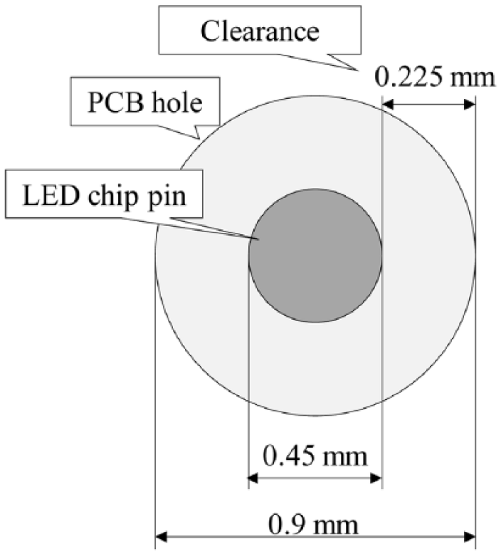
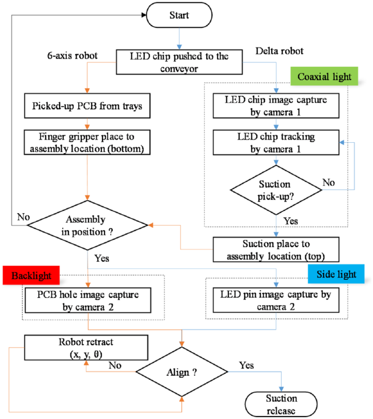
The purpose of this work is to automate the assembly of the DIP components such as the insertion of an LED DIP chip within a PCB assembly (Figure 1). As shown in Figure 1(b), the PCB consists of multiple-hole components in which each component has circles with a different set of radii. As shown in Figure 1(a), a DIP LED chip with multiple pins placed on the outer surface is inserted within the PCB holes of Figure 1(b). However, the chip pins are not generally aligned in parallel. As shown in Figure 2, the radial assembly clearance between the pin and a hole ring is 0.225 mm. The robotic LED chip mounting system consists of a delta robot located immediately above the placement table surface, a six-axis robot arm to pick up the PCB from the tray, the first camera (camera 1) to measure the relative position of the LED chip, and the second camera (camera 2) to provide feedback on the PCB position. The delta robot and six-axis robot are developed by Industry Technology Research Institute (ITRI) 17 and operate in the closed-loop position control 18 for a robot manipulator based on visual feedback measurement. The camera for each of the units was a complementary metal-oxide semiconductor (CMOS) sensor with a resolution corresponding to 752 × 480 pixels and an image capture rate of 60 fps. Cameras were mounted on the Azure lenses with a focal length of 12 mm. A vacuum generator was employed to suck the LED chip. The lighting system consisted of a white backlight and two LED ring lights with white and blue colour illumination as shown in Figure 3. In order to synchronize two independently operating robotic systems, a software solution was proposed in the study that enables a delta robot and a six-axis robot arm to be temporally and spatially synchronized using single PC communications.
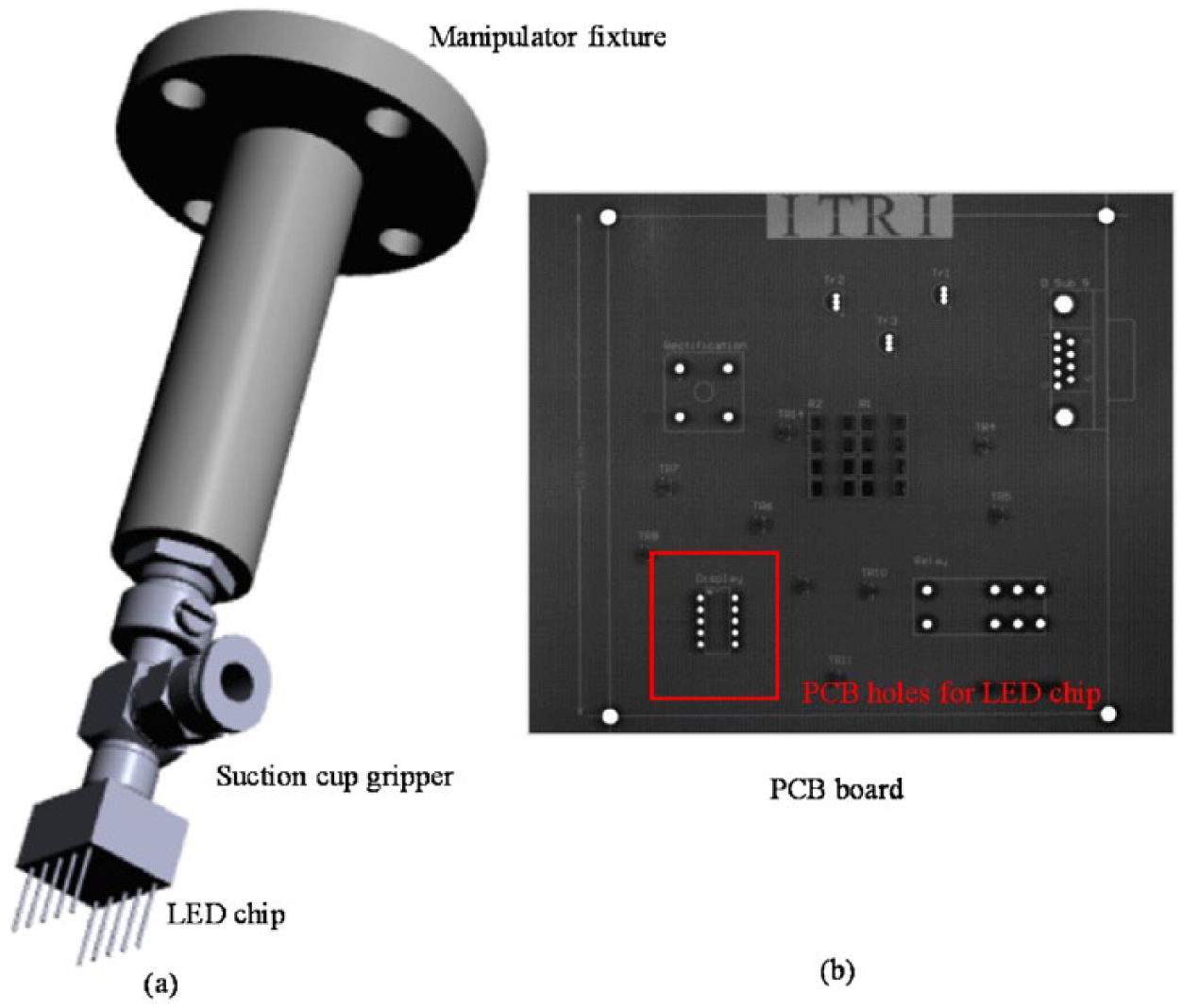
Schematic for mounting LED chip on the PCB (a) a DIP LED chip and (b) the PCB board.
Configuration for mounting space description.
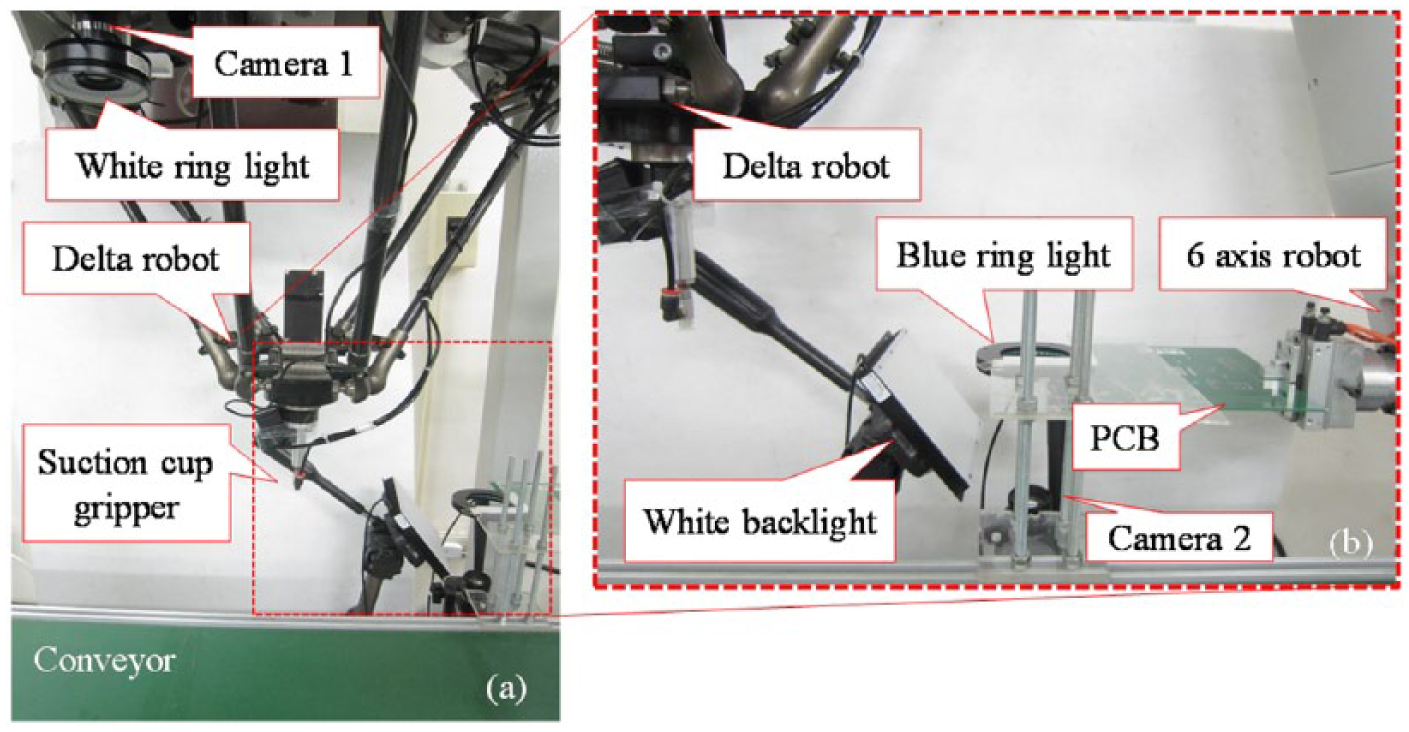
Robotic in-process LED chip mounting system that consists of a six-axis robot arm, a delta robot, two charge-coupled device cameras, and two lighting system setups (a) a white ring light and (b) a white backlight and a blue LED ring light.
The chip mounting procedure is broken down into two steps, namely, to identify and track the LED chip from the conveyor and to place the LED chip to match the PCB hole. Two lighting system setups were used in the chip mounting procedure as shown in Figure 3(a) and (b). The proposed procedure operates in sequence. After the parts are pushed to the conveyor in sequence, the first camera (camera 1) searched the moving objects continuously and located the position of the LED part, while the part moved to the region of interest (ROI). Initially, the image (Figure 4(a)) of the LED section was acquired after switching on the white ring light. The features of the LED chip were extracted from the image. After the vision localization, an LED chip was selected from the conveyor by a suction cup gripper, moved from the pickup location, and subsequently stopped on the assembly location. The image processing method for the pin-in-hole feature extraction is discussed in the next section.
Images of the (a) LED section, (b) 10 connected pins, and (c) PCB surface.
The LED chip is contained in a DIP and involves 10 pins. Subsequently, the image (Figure 4(b)) of the 10 connected pins of the LED chip was acquired by the second camera (camera 2) after switching on the blue ring light system below the connected pins of the LED chip. Similarly, a PCB was selected by a six-axis robot arm from the tray and firmly clamped by the gripper with the two opposing fingers. The PCB was moved from the pickup location to the assembly position beneath the LED chip and was parallel to the bottom of the LED chip. Finally, the two parts are positioned in place and an underlying white backlight is placed to ensure maximum uniformity of white illumination for the PCB surface (Figure 4(c)). The positions of the PCB holes were detected using the second camera (camera 2) to provide feedback and begin the assembly operation. During the feedback adjustment, the LED chip is stationary, while the PCB is moved by retracting the six-axis robot. The assembly is accomplished by a three-dimensional (3D) motion of the PCB position, and the final position corresponds to where the PCB holes correctly mate with the chip pins. The position was calculated from the relative position of the parts in the robot space. After the successful completion, the assembled PCB was subsequently placed on an output tray. Figure 5 shows the flow chart of the developed robotic in-process LED chip mounting system operation.
Operation sequence of the robotic in-process LED chip mounted into a PCB.
Lighting system and image processing
The lighting technique is essential for the automated assembly system and especially while measuring the sizes or positioning the elements. 19 Improper lighting creates a noisy image and ensures that thresholding is more critical and thus results in inherent measurement uncertainties. Figure 6 shows three different lighting types, namely, front lighting (i.e. white ring light), backlighting (i.e. white backlight), and side lighting (i.e. blue ring light). With respect to different assembling steps, it is necessary to select proper illuminations to highlight the feature image on the object surface. Front lighting is selected using coaxial lighting, and the captured image is shown in Figure 6(a). The top face of LED is clearly observed even if the surface is dark. With respect to the LED pin part, the small pin tips on the LED surface are conspicuously observed while using the side lighting as shown in Figure 6(b). As shown in Figure 6(c), the PCB hole features are highlighted using the backlighting. Although noisy features appear, we use the image processing technique to remove the same. Based on the above-mentioned analysis of the pin–hole detection, a software program for pin–hole assembly is developed in C++ for a PC with 2.6 GHz CPU and 4 GB RAM.
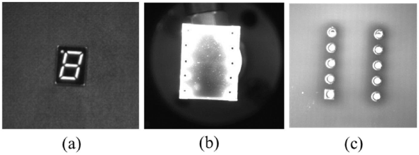
Images illuminated by (a) coaxial light, (b) side light using a blue ring, and (c) backlight.
The sequence of the image processing for the pin–hole feature extraction is illustrated in the flow chart in Figure 7. The pin–hole assembling process requires aligning the chip pins with the holes on the PCB. In the automated assembling system, the bottom pins of the chip move and align the inner circumference with the holes on the PCB. Thus, the features of pins and holes should be defined and extracted by applying the image processing algorithms to the image acquired by the two cameras. In the case of the LED chip, the features correspond to the top surface for sucking placement identification and mounting pins beneath the chip. The correspondence of pin in hole is determined by the position of the pins and the hole shape.
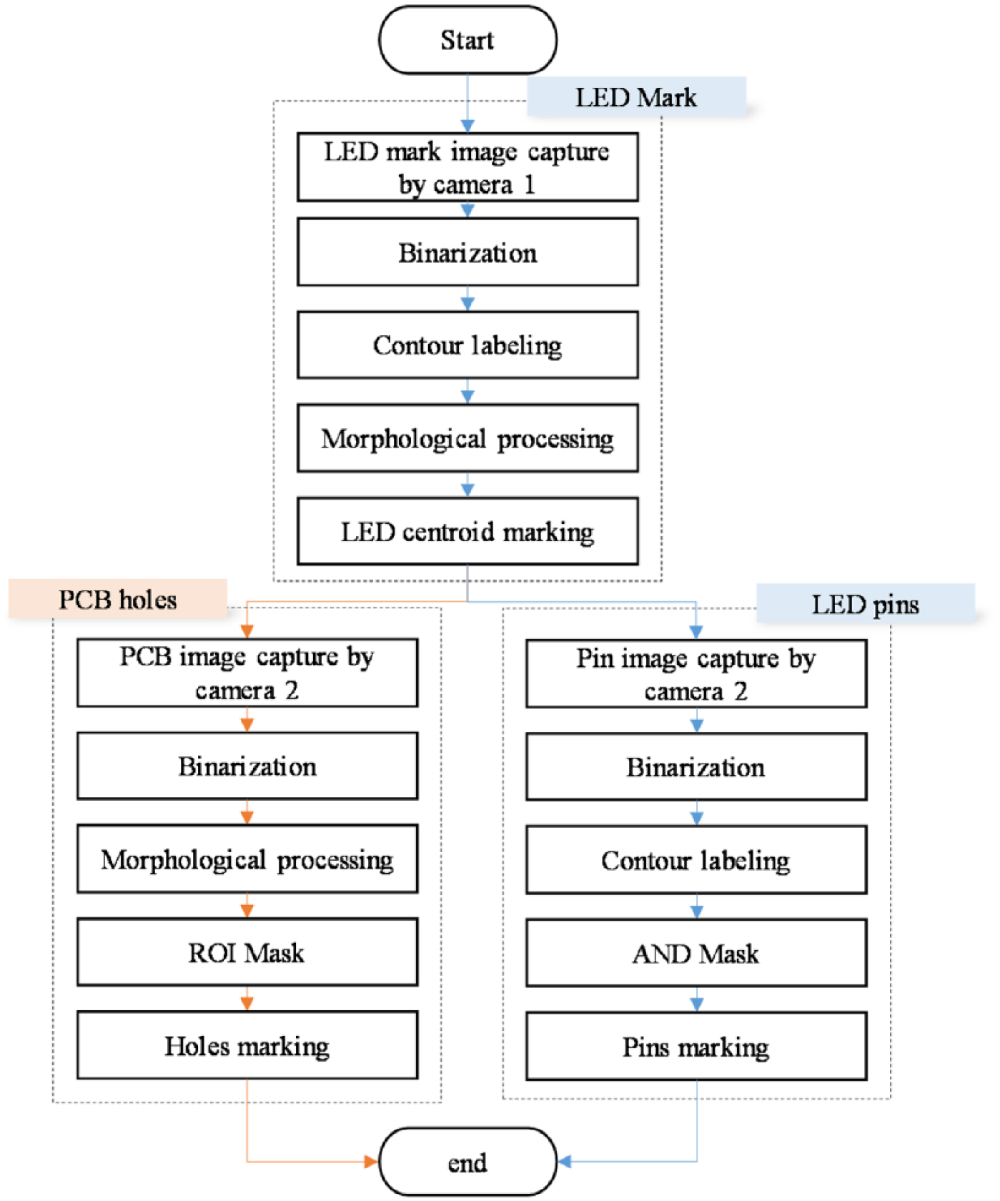
Image processing sequence for the pin-in-hole feature extraction.
Figure 8 illustrates the image processing for each process to extract the mark of the LED chip. Initially, image binarization is applied to the acquired image shown in Figure 8(b). Following the binarization process, the grey levels were inverted as shown in Figure 8(c). The outer contours were extracted as shown in Figure 8(d). Subsequently, the disconnected contour is given by the bitwise AND operation between Figure 8(b) and (d). The morphological processing of the binary result improves the mark identification. The morphological operation is performed with the erode operation to fill the hole (Figure 8(g)) and follows the dilate operation to remove outer boundary pixels without holes (Figure 8(g)). After the morphological process, the results detect the centroid position of an LED chip image as shown in Figure 8(h). The processing time for one image is approximately 70 ms, and this is sufficiently fast to satisfy the feed rate of the parts.
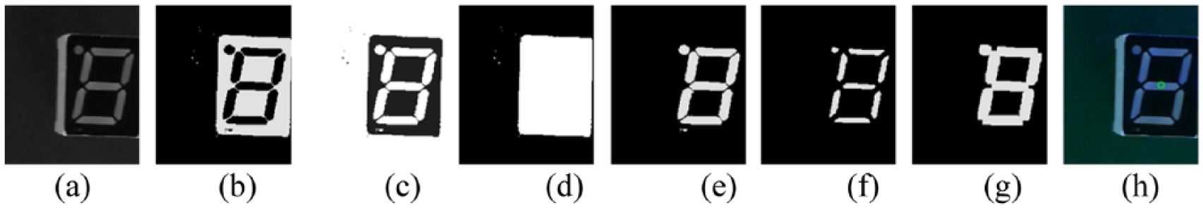
Image processing steps for the mark feature extraction of the LED chip: (a) grayscale image; (b) binarization; (c) complement image; (d) determining external contour; (e) bitwise AND of (b) and (d); (f) erode operation; (g) dilate operation; and (h) result.
Figure 9 illustrates the image processing for each process to extract the pins of the LED chip. Initially, image binarization is applied at the acquired image shown in Figure 9(b). Following the binarization process, the grey levels were inverted as shown in Figure 9(c). The outer contours were extracted as shown in Figure 9(d). Subsequently, the disconnected contour is given by the bitwise AND operation between Figure 9(c) and (d). After the AND mask process, the results detected each pin diameter (i.e. φpin) and pin position of an LED chip image as shown in Figure 9(f). The processing time for an image is approximately 85 ms, and this results in significant time saving.
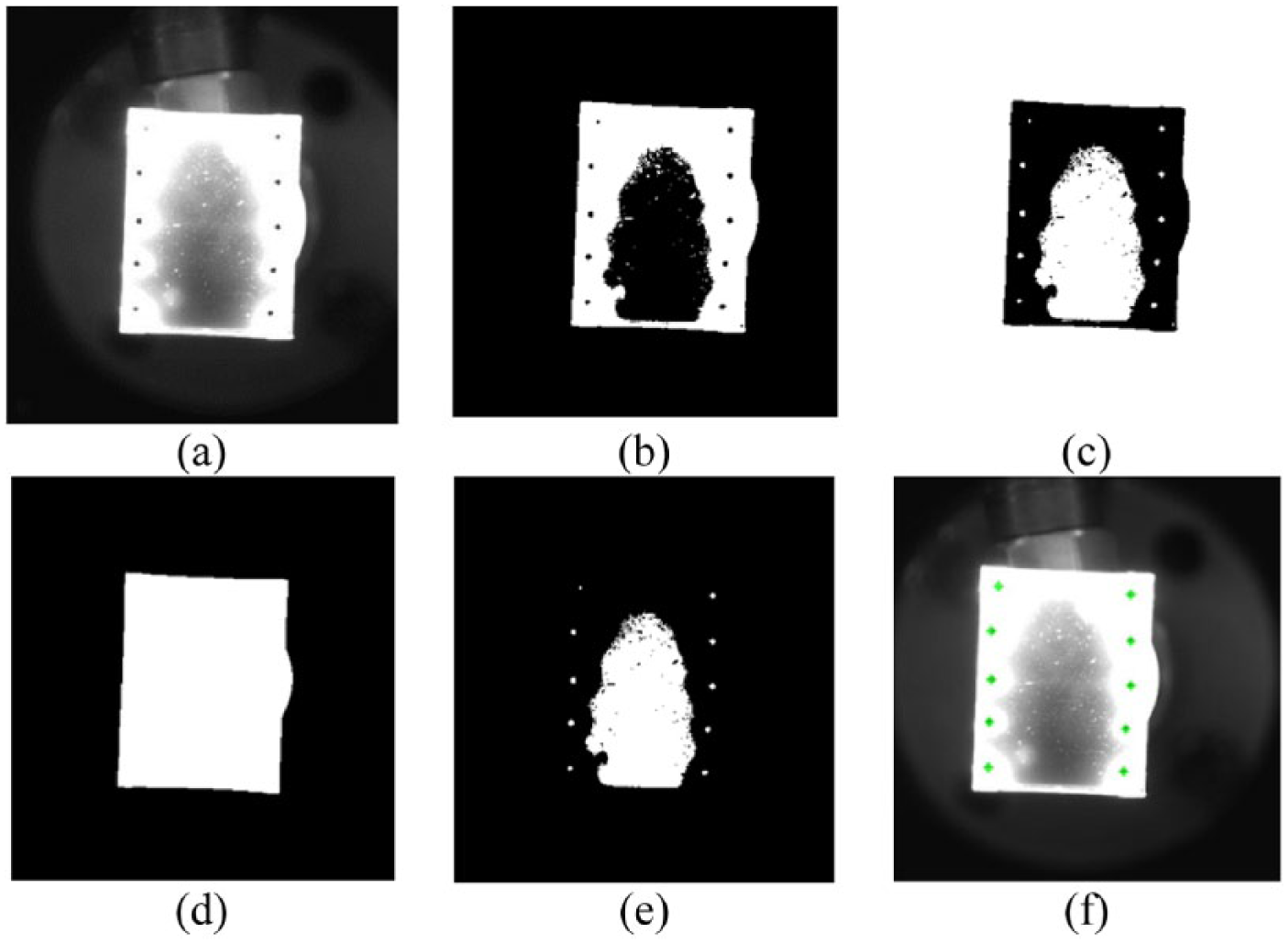
Image processing steps for the 10-pin feature extraction of LED chip: (a) grayscale image; (b) binarization; (c) complement image; (d) determining external contour; (e) bitwise AND of (c) and (d); and (f) result.
Figure 10 shows the image processing for each process to extract the holes of the PCB. Initially, image binarization is applied at the acquired image shown in Figure 10(b). After the binarization process, the morphological operation was performed with the erode operation to fill the spot (Figure 10(c)) and is followed by the dilate operation to remove outer boundary pixels (Figure 10(d)). Subsequently, the uneven pixels are eliminated by the bitwise AND operation between Figure 10(d) and defined ROI. Furthermore, the results detected each hole diameter (i.e. φhole) and position of a PCB image as shown in Figure 10(f). The processing time for one image is approximately 85 ms in a computationally efficient manner.
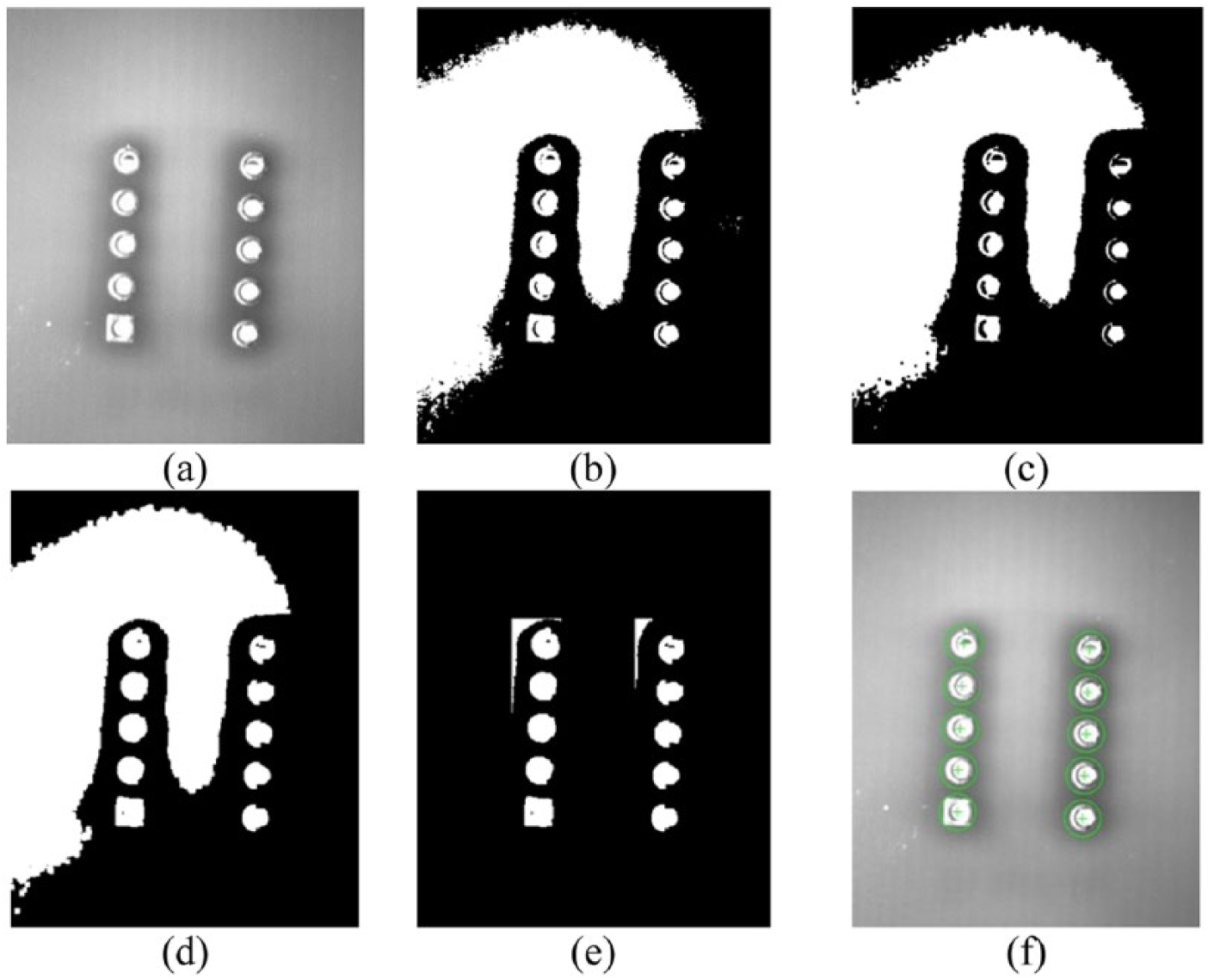
Image processing steps for the hole feature extraction of PCB: (a) grayscale image; (b) binarization; (c) erode operation; (d) dilate operation complement image; (e) masking of (d) with ROI; and (f) result.
Uncertainty evaluation
In order to determine the uncertainty of automatic mounting for LED devices, the concept of the ‘uncertainty budget’ 20 was adopted to determine the composition of the standard uncertainties of all the important factors. After performing a repeated test motion with a distance of 352 mm from 29 repeated tests for the delta robot, the standard deviation of uΔ was 0.02. The standard deviations of the sucking position in the x- and y-directions by the vacuum generator from five repeated tests were 0.08 (i.e. us,x) and 0.18 (i.e. us,y) mm, respectively. The tolerances of the pin-to-pin spacing distance for dual in-line LED package range within ±0.1 mm. Both the tolerances of the hole size and position for PCB range within ±0.1 mm. With respect to the measuring devices that are used for statistical process control, the measurement uncertainty should not exceed 1/20th of the available tolerance. Hence, the equivalent measurement uncertainties of ut for dual in-line LED package and PCB were 0.01 mm. While composing the uncertainty budget, the combined measurement uncertainty uc is calculated from the pin-to-pin distance of LED and individual x- and y-axis uncertainty contributions by the application of the error propagation law as given by the following equation
The uncertainty uc is 0.20 mm. The pin diameter for the 10-pin LED chip is 0.45 mm. The hole diameter for PCB is 0.90 mm. Hence, the permissible position tolerance between the pin size of LED and the hole dimension of PCB is 0.45 mm. The 10-pin LED chips are individually capable of sliding independently in the horizontal plane by up to 0.45 mm and rotating about a vertical axis. The PCB holes for LED chip pins are a tight fit, and in total 10 pins are mounted to the PCB. However, the expanded uncertainty is ±0.4 mm and results from uc from twice the standard deviation (level of confidence of 95%). The expanded uncertainty range between the upper and lower limits was out of the tolerance range. Thus, the radial assembly uncertainty is more than 1.8 times the clearance required for success. A comparison of the measurement uncertainties determined with the maximum permissible values shows that it is not possible to mount the LED chip on the PCB confidently for the given conditions. In addition, the outlier pin should be aligned with the z-rotation of the centroid LED chip within 35 mrad to ensure successful assembly to the outlier PCB hole although the pin spacing is 2.54 mm between the in-line pins. The assembly allowance in the angular position between the PCB holes and LED chip pins is arbitrarily low.
Visual servoing feedback with uncertainty compensation
In order to compensate for the varying position and misalignment errors and snap fit the tolerance during the pick and place operation, the visual servoing is employed to guide the robot with a closed-loop control. As shown in Figure 11, the features of the 10 connected pins of LED chip (Figure 11(a)) and the 10 holes on the PCB (Figure 11(b)) are extracted from the image of the camera. Figure 12(a) shows the captured image when the LED chip approaches the PCB surface. The green circle shows that a connected pin of LED chip is within the zone of a PCB hole. However, the red circle denotes that a connected pin of LED chip is out of the region of a PCB hole. Due to the position errors, neither the LED chip nor the PCB is at the assembly corresponding position. The positional errors include both plane and rotational directions. A demonstration video of our experiments without the visual servoing feedback is available at https://youtu.be/j9dyeldWQX4.
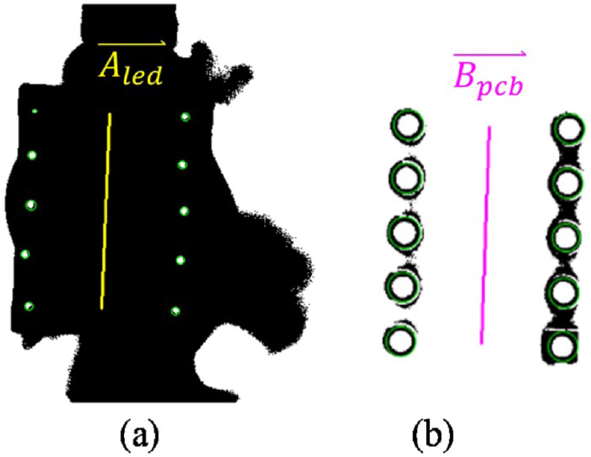
Feature extraction for the (a) 10 connected pins of LED chip and (b) 10 PCB holes.
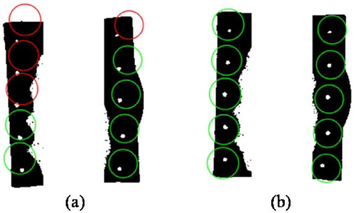
LED chip mounting state (a) before and (b) after the visual servoing was employed.
For robot autonomous execution, the proposed insertion strategy decouples the insertion process into the plane adjustment phase and orientation adjustment phase and controls them separately. Thus, the pin-in-hole problems pose an insertion strategy in three dimensions as follows: relative position in the plane and relative orientation about the vertical axis. The central line in yellow (i.e.
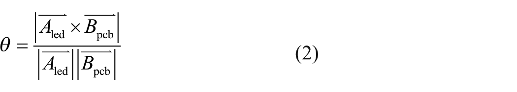
and yields the orientation θ to align the two central lines.
The close initial alignment of pins with holes is conducted by aligning the orientation of the central yellow and purple lines and rotational angular displacement within the calculated degree θ. In order to line up the LED chip with the hole on the PCB, the position in the x- and y-directions is moved by overlapping the centroids of the pins and holes, respectively. After the alignment, the delta robot releases the LED chip directly down towards the PCB. Figure 12(b) shows the result after visual servoing feedback is applied to the chip mounting process.
However, a single feedback insertion strategy may not yield the precise location of x and y and orientation of θ of the pin–hole required for assembly due to the edge uncertainty 5 caused by uneven illumination variation. 21 Hence, the uncertainty on the edge localization directly influences the centroid position of the pin and hole. Examples of sets from three actual experimental results are shown in Figure 13. The LED pin tip is represented as a red solid circle, while the PCB hole is denoted as a green circular ring. As shown in the acquired images from camera 2, all the 10 pins of LED were located within the PCB holes in all the three cases. However, the successful insertion tasks are fulfilled in Figure 13(a) and (b) although Figure 13(c) reveals the failure of the insertion operation.
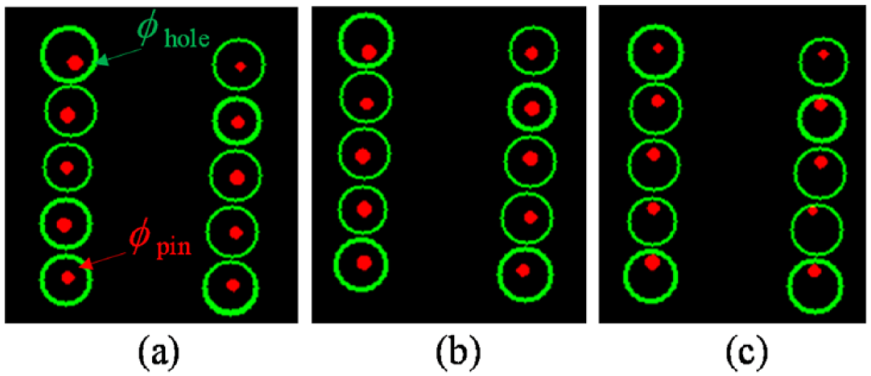
Experimental data sets acquired from the individual pin–hole insertion measurement: (a) successful assembly, (b) successful assembly, and (c) unsuccessful assembly.
Currently, the feedback insertion strategy is performed to acquire a good initial approximation to the pin–hole location and subsequently shift the control to lighting uncertainty–compensated strategy to achieve fully reliable assembly. Although the feedback strategy eliminates all the position errors accumulated during the assembly operation, the strategy is unable to compensate for the inaccuracy of the robot and inherent and unavoidable errors of the vision system. 8 The uncertainty-compensated strategy uses a compliant mode to accommodate the remaining lighting errors. As shown in Anchini et al., 21 the uncertainty for the edge positions was always within ±1 pixel from the most frequent position.
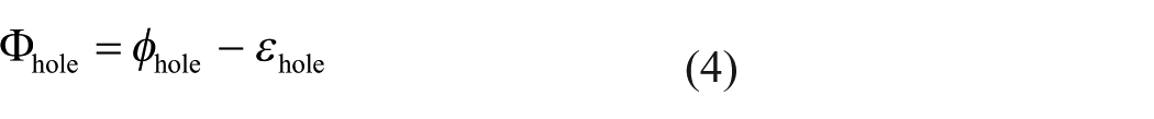
In order to accommodate the insertion uncertainty at a pin-in-hole position, our strategy involves applying the uncertainty evaluation method depicted in the previous section. The new pin diameter Фpin after uncertainty compensation is given as follows
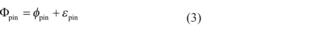
where εpin denotes the remaining lighting error. The pin diameter is added on the known uncertainty contour εpin around the outer pin that yields another set of pin profiles to present the candidate sets. Therefore, the pin diameter of LED pin is increased to present the equivalent measurement uncertainty influence for the LED part. The radius of the PCB hole φhole shrank with the uncertainty contour. After combining the uncertainty information, the hole size (i.e. φhole) of the PCB is reduced to present the uncertainty influence of hole size and position for the PCB. The new hole diameter Фhole after uncertainty compensation is given as follows
where εhole denotes the remaining lighting error. From the uncertainty space viewpoint, determining x and y coordinates of the pin with a diameter of Фpin that satisfy adequate concentricity within the diameter of Фhole (within the assembly clearance) corresponds to determining coordinates that lie outside a circle with the diameter Фpin located anywhere within a bound of diameter Фhole. Thus, the pin–hole candidate sets yield a lower assembly clearance. Figure 14 shows the experimental data sets after combining the uncertainty information. Figure 14(c) reveals a slight overlap between the pin tips and hole rings that produces a high contact force that causes the LED pin to get stuck during insertion. Therefore, insertion error occurs due to the uncertainty caused by the illumination variation and the inaccuracies in the centroid position.
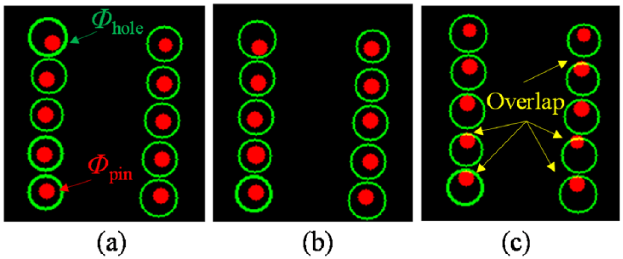
Experimental data sets after combining the uncertainty information: (a) non-overlapping, (b) non-overlapping, and (c) overlapping marked in yellow.
The uncertainty contour information is added, and thus the system performs the second attempt of insertion. The second pin–hole insertion parameters of (x′, y′, θ′) generated from the uncertainty contour are used with successive insertion movements to determine the correct position and orientation of the hole. After the PCB reaches the second pin–hole insertion position, the robot subsequently intentionally retracts the PCB some distance in each of the x- and y-directions. The range of retract motion is determined such that overlapping by considering the maximal possible overlapping ranges between the LED chip and the PCB hole ring. The range is easy to select and is very conservative as long as the overlapping areas disappear. Subsequently, we may continue to obtain uncertainty contours at various control positions to retract robot movement and finally arrive at non-overlapping combination. The LED chip and the PCB are already aligned, and thus the snap fit is assured. A demonstration video of our experiments with the visual servoing feedback is available at https://youtu.be/PjzOf1v7m5g. The use of vision sensors in feedback loop reliably compensates for the system uncertainty. The proposed uncertainty-compensated strategy measures the clearance margin from the uncertainty information between the hole ring and LED pin based on vision inputs and uncertainty configuration. The essential contribution of the proposed method is that the feedback insertion strategy in conjunction with uncertainty-compensated strategy to align two parts accurately and automatically compensates for the inaccuracy of the robot.
Conclusion
In this study, a machine vision–based system was proposed for in-process LED chip mounting. The system was realized by designing the optimal lighting solution and using off-the-shelf hardware and software. The uncertainty of the LED chip mounting process was analysed in detail. Computationally efficient and robust implementations of the image capturing and processing components enabled reliable real-time visual online position feedback and high-speed grabbing operations using a delta robot manipulator. Uncertainty compensation–based insertion strategies for pin-in-hole assemblies were implemented to accommodate the uncertainty errors. Overall, the proposed uncertainty compensation strategy along with the robotic in-process LED chip mounting system and on-line feedback is realized as a straightforward implementation and is effective for electronic manufacturing industries.
Footnotes
Acknowledgements
Special thanks to anonymous reviewers for their valuable suggestions.
Declaration of conflicting interests
The author(s) declared no potential conflicts of interest with respect to the research, authorship, and/or publication of this article.
Funding
This study was supported by the Ministry of Science and Technology, Taiwan under Grant No. MOST 106-2622-E-027-014-CC3.