
Abstract
Titanium alloys are known to cause crater wear on cutting inserts. It is one of the life-limiting factors for the tool life and highly influenced by the cutting parameters. To increase productivity, there is a strong incentive to increase the production speed. At the same time, the tool life should be unchanged or even prolonged.
The influence of cutting speed, feed and cutting length on wear was investigated in turning tests using cemented carbide inserts and titanium alloy Ti6Al4V as work material. The results showed a very strong influence from all parameters on crater wear, confirming previous findings reported in the literature. The resulting wear surfaces were studied in detail, revealing a crater filled with transferred titanium alloy. The tungsten carbide grains underneath were depleted of carbon, resulting in a nano-rough top surface rich in tungsten. In addition, the turning tests showed a threshold cutting speed, below which no crater wear occurred.
Introduction
During the past decades, there has been an intense development of new tool materials for metal cutting in general, including the introduction of several types of ceramic coatings. As a result, uncoated cemented carbide inserts are now rarely used in turning of metallic materials. Many attempts have been made to introduce coated inserts also in the cutting of titanium and its alloys, but it has yet not succeeded [1–4]. Due to the high reactivity between titanium and most ceramic coatings, together with the low fracture toughness and low thermal conductivity of the coatings, uncoated cemented carbides are frequently used [1,3,5]. Other types of ceramic tool materials such as polycrystalline diamond, polycrystalline boron nitride and cubic boron nitride have been successfully implemented in specific titanium cutting applications, exemplified in [1,5–7], but are not widely used due to an increased cost and limitations in toughness.
In Refs. [1,5], some important criteria of a successful tool material for cutting titanium are mentioned. To limit problems with heat generation, a high hot hardness, high thermal conductivity and low chemical affinity to titanium is needed (also at elevated temperatures). To minimize the risks associated with chip formation, a high toughness, fatigue resistance and high compressive strength is required. There is no available material that fulfils all of these criteria, but cemented carbide is performing well in many of the above-mentioned areas. Although uncoated cemented carbides have proven their superiority in the application, the wear is relatively high and is reported to be characterized by notching, thermal diffusion, chemical reaction, crater wear, abrasion and chipping, and subsequent catastrophic failure is not uncommon [1,4,8,9].
Crater wear is one of the limiting factors for the tool life and occurs on the rake face of the cutting tool inserts, which is exposed to the fresh titanium chip. High cutting speed, high feed and large cutting depth are all known to increase the wear rate, and hence decrease the tool life, drastically [1,4,8–13]. Today, straight WC/Co grades containing 6–10 wt% Co is commonly used at low cutting speeds, to extend the tool life as much as possible [1–3,7–9]. However, to increase productivity and minimize material consumption, there is a strong incentive to increase the cutting speed, while the tool life should be unchanged or ideally prolonged.
Higher cutting speeds generate higher temperatures in the contact between the chip and the rake face [4,12,14]. When turning metals with higher thermal conductivity, e.g. steel, most of the heat is transported out of the contact by the continuously renewed chip. However, due to the low thermal conductivity of titanium alloys and a relatively short chip-tool contact length, a larger proportion of the heat remains in the contact (about 80% when machining titanium alloys, to compare with 50% for steel) [1,5]. This leads to temperatures above 600°C on the rake face already at a low cutting speed of 50 m/min and increasing the speed to 250 m/min causes the temperature to rise above 1000°C [11]. At such high temperatures, titanium diffuses into the tool and modifies its surface properties. Also, diffusion of both tungsten and cobalt into the chip is believed to play an important role in the rapid wear of the tool. Further on, titanium becomes very reactive at these elevated temperatures generated in the secondary shear zone and the tool is deteriorated [1].
Diffusion of titanium into cemented carbide, as well as tungsten, carbon and cobalt into titanium, has been shown in [15–18] using a diffusion couple method. The diffusion of cemented carbide constituents into the passing chip is, however, hard to prove in the cutting application due to the presumed low amount of W, C and Co in relation to the large amount of titanium in the chip. It has been suggested that formation of a stable reaction layer of TiC at the tool–chip interface increases the diffusion length between chip and tool and decreases the wear rate. Also, an adhered titanium layer on the tool, separating the tool from the flowing chip, might protect the tool from further wear [1,4,14,19,20].
The present study focuses on investigating the wear and potentially protective layers further by detailed wear surface studies, using novel surface analysis techniques. The influence of cutting parameters on surface appearance has also been investigated.
Experimental
Materials
Cutting inserts
Uncoated cemented carbide cutting inserts were used for turning with different cutting parameters, followed by characterization of the wear surfaces. The inserts were made of grade H13A (6 wt% Co, 94 wt% WC, 1 µm mean WC grain size), commonly used in turning of titanium. The inserts are of type TPGN160308, flat without chip breakers, to function as model inserts (see Figure 1). Each insert is prepared by grit blasting, using Al2O3, of the surface to remove the sinter skin. The roughness of the achieved surface is measured to Ra 0.30 ± 0.02 µm (measured using white light interference profilometry over a surface of 45 × 59 µm, average of 10 measurements).
(a) A cutting insert of type TPGN160308 mounted in the holder of type CTDPR 2525M16. (b) Sketch showing the cutting insert and studied wear area. The length of one edge of the triangular insert is 15 mm.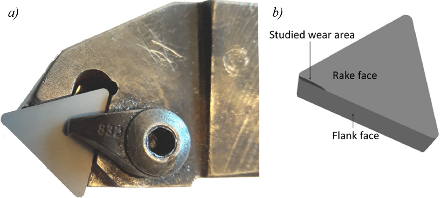
Immediately before testing, all cutting inserts were ultrasonically cleaned in hexane followed by ethanol for 3 min, respectively.
Composition of Ti6Al4V (wt%).
Composition of Ti6Al4V (wt%).

Varied parameters during the cutting tests.
Varied parameters during the cutting tests.
Low corresponds to 40 m/min, medium to 70 m/min and high to 100 m/min.
Normal corresponds to 0.15 mm/rev and high to 0.30 mm/rev.
All surfaces were imaged and analysed using scanning electron microscopy (SEM; Zeiss Merlin), energy-dispersive X-ray spectroscopy (EDS; Oxford X-max) and white light interference profilometry (WYKO NT1100) after the cutting tests. Cross-sections were produced in selected areas by focused ion beam (FIB; FEI Strata DB235).
Subsequently, one sample for each setting was immersed in hydrofluoric acid (HF) etchant to remove any present transferred work material, before repeated analysis by SEM, EDS and white light interference profilometry. The etchant HF reacts solely with the metallic titanium alloy adhered on the surface, revealing the worn tool surface underneath. Selected etched surfaces were additionally characterized with atomic force microscopy (AFM; PSIA XE-150).
Results
Wear characterization
Three repeated tests were performed using medium speed, normal feed and a cutting length of 200 m (MN200). After testing, the cutting edge and rake face was covered by titanium alloy, exemplified in Figure 2. The transfer layer was generally quite smooth, but with larger chunks of titanium alloy adhering along the cutting edge and, more prominently, along the transition region, where the chip separates from the insert.
Rake face of MN200 after test (SEM, 3 kV).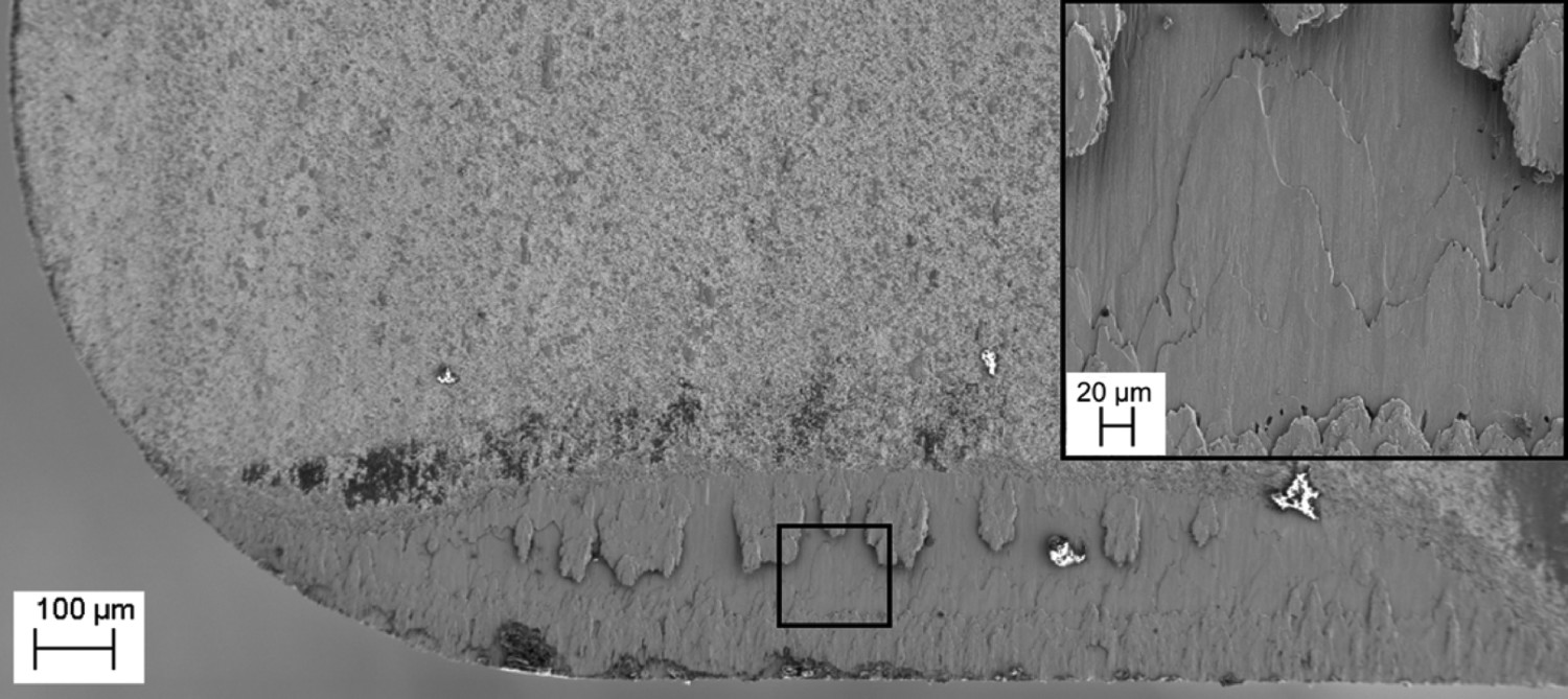
The corresponding chip was segmented and approximately 160 µm thick (see Figure 3). On the side sliding against the rake face, small particles/chunks of titanium alloy could be found on top of the otherwise smooth chip.
Chip from cutting with medium speed and normal feed (MN200). (a) Side view, the bottom part has been sliding against the rake face, (b) the surface that has been sliding against the tool surface and (c) the segmented top of the chip (SEM, 3 kV).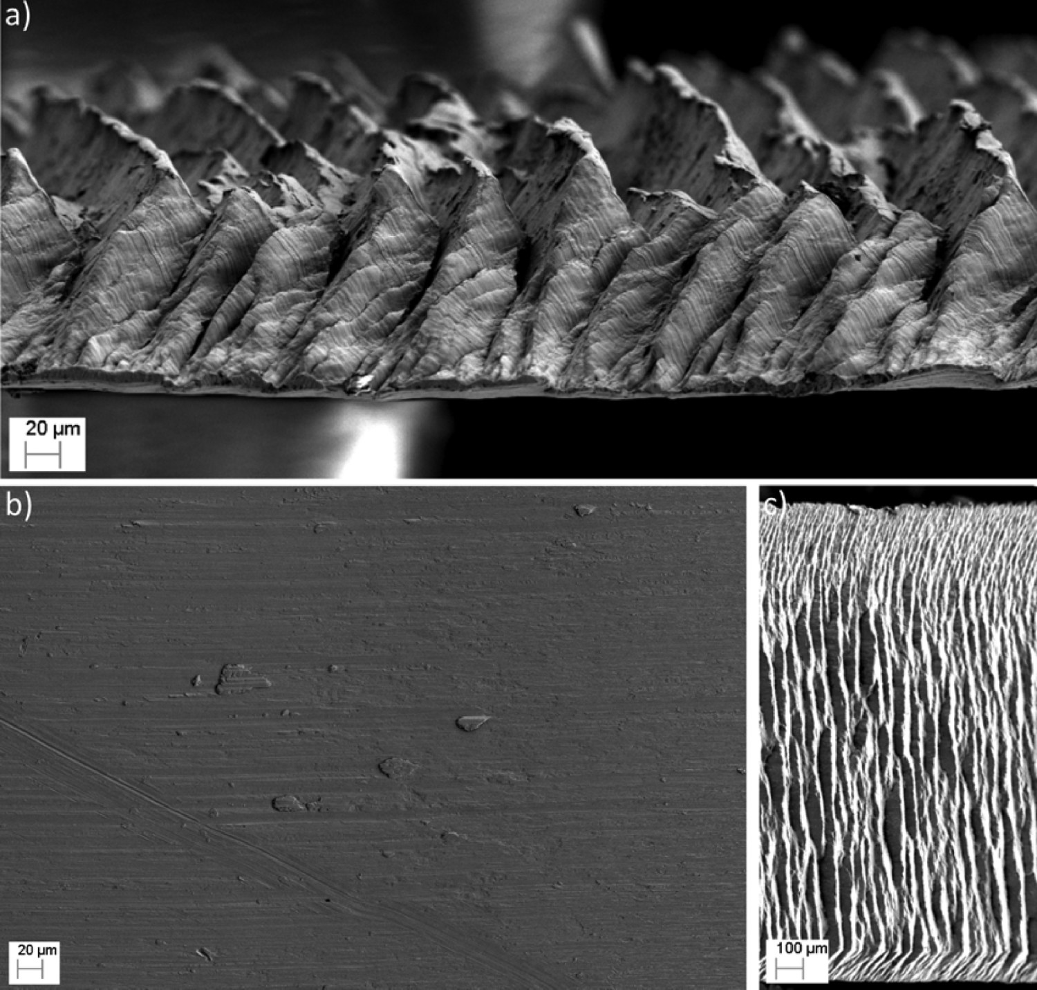
To be able to measure the wear, one sample was immersed in HF, until all titanium alloy on the surface was removed. After the etching process, an area much brighter than the original cutting insert was observed, extending about 285 µm from the cutting edge (see Figures 4 and 5). Studying this area in higher magnification (see Figure 4(b and c)) and in tilted view (see Figure 4(d and e)), it was found that this area constitutes a crater. Besides that, the cutting edge became slightly rounded and in the bottom of the crater, the binder separating the WC grains was removed. The WC grains also had a rough appearance on a very small scale.
MN200 after test, subsequently etched in HF. (a) Overview, (b) transition region, (c) bottom of crater, (d) overview tilted and (e) bottom of crater tilted (SEM, a-c 3 kV, d-e 10 kV). MN200 after test and subsequent etching in HF. (a) Tilted view (SEM, 10 kV) and (b) corresponding white light interference profilometry measurement.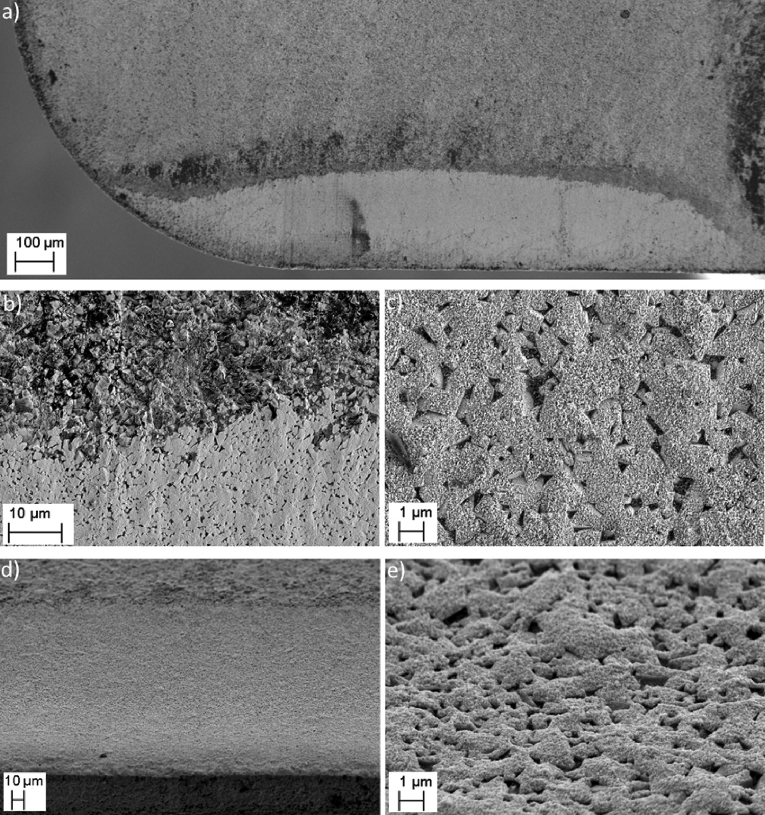
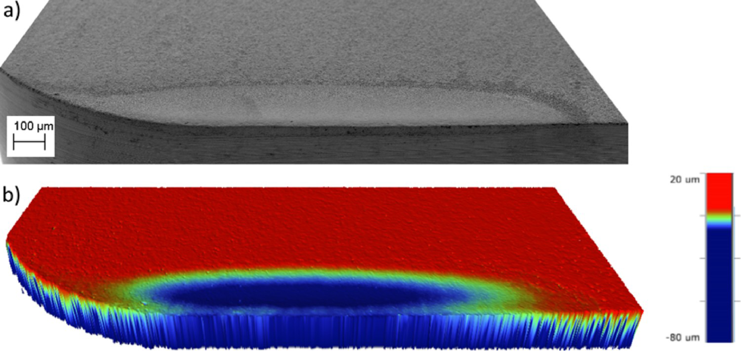
The depth of the crater was measured by white light interference profilometry, shown in Figure 5, and a maximum depth of 15 µm was recorded in the most affected zone.
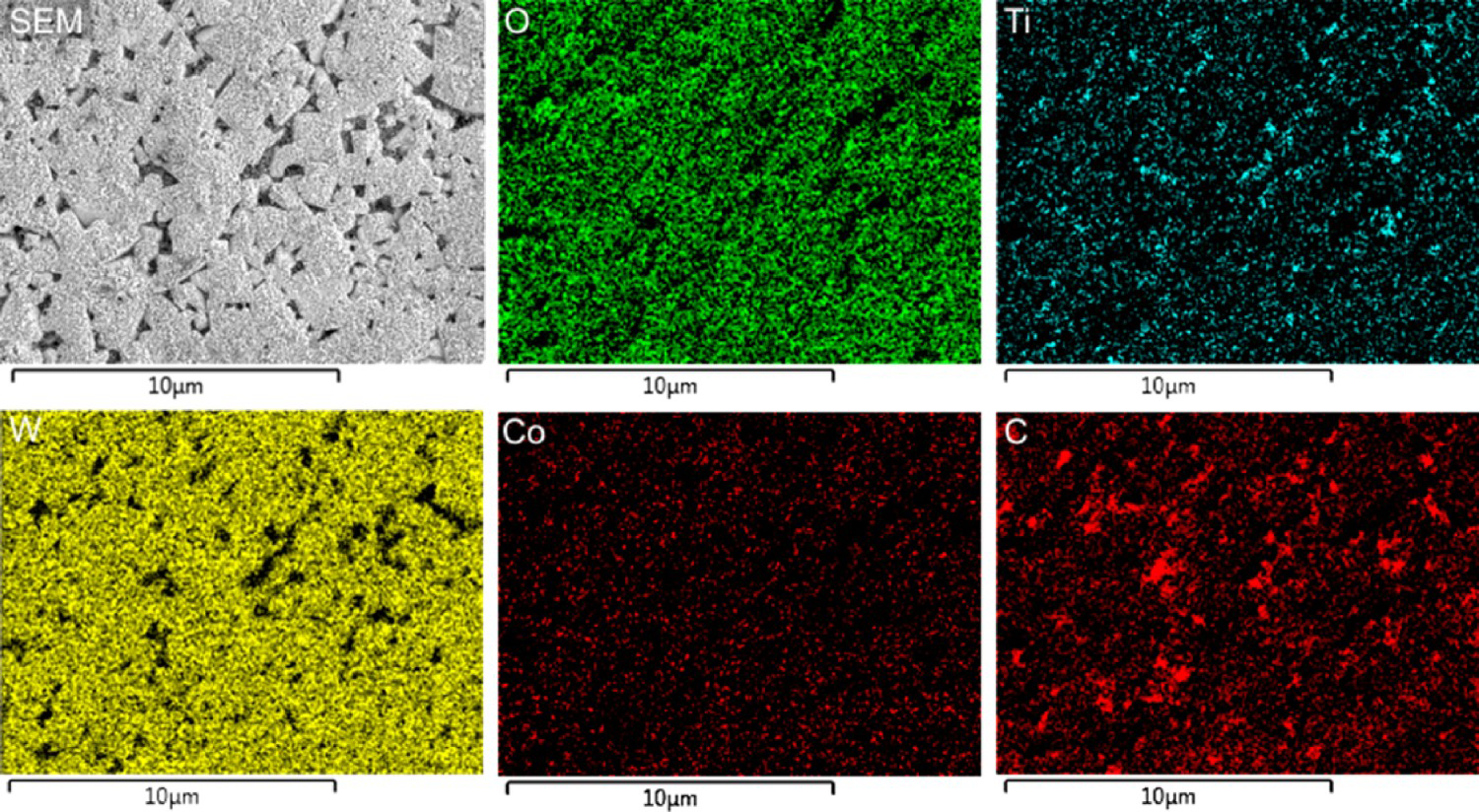
Using elemental analysis, see Figures 6 and 7, the presence of Ti and C in between WC grains could be observed, as well as carbon depletion in the WC grains (confirmed by a relatively low amount of C in an area recognized as WC grain in the SEM image).
MN200 after test and subsequent etching in HF. (a) SEM image, where the positions for elemental analysis are indicated. (b) Elemental analysis in position I (black solid line). Corresponding analysis of a WC grain outside the wear mark is given (light grey dashed line) for comparison. (c) Elemental analysis in position II (SEM and EDS at 3 kV). Elemental analysis of MN200 after test and subsequent etching in HF (SEM and EDS at 3 kV).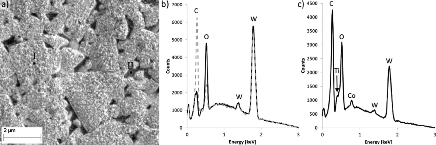
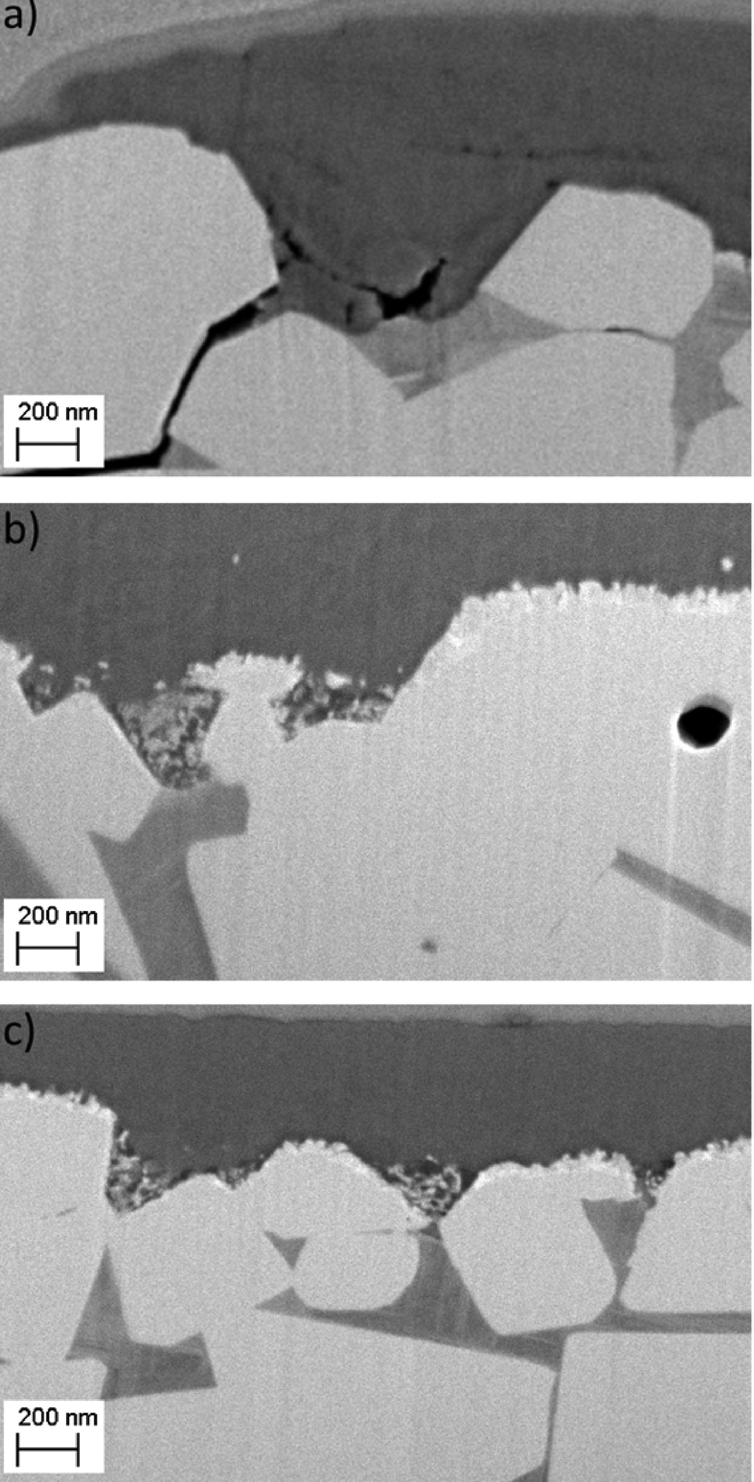
In the cross-section of a non-etched tool, see Figure 8, it was revealed that the worn cemented carbide surface is actually quite smooth underneath the transferred titanium alloy, although several microns (corresponding to several layers of WC grains) have been removed. The small-scale pattern on top of the WC grains could be observed underneath the approximately 2 µm thick transfer layer of titanium alloy. A few hundred nanometres deep pits separate the WC grains in the worn cemented carbide surface (see Figure 8(b)). These pits were partly filled with darker material, including wear fragments appearing bright in the SEM. Cobalt, which constitutes the binder of the cemented carbide, is visible below the dark material in the pits. The transferred titanium also includes occasional nanometre-sized wear particles (see Figure 8(b)).
FIB cross-section of MN200. (a) Combination of top view and cross-section and (b) close up of cross-section detail indicated in (a) using in lens secondary electron detector (SEM, 3 kV).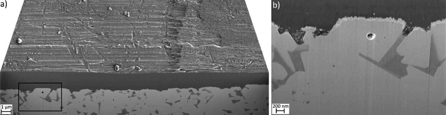
To get an idea about the wear progress, a test to 100 m was performed (as compared to 200 m). The sample showed similar features as MN200 (see Figure 9), but the crater wear depth was much smaller. The most affected part had a wear depth of 4 µm. Also, the final contact length was shorter, indicated by a crater extending 220 µm from the cutting edge.
MN100 after test. (a) overview, (b) overview after subsequent etching, (c) white light interference profilometry measurement corresponding to the area imaged in (b), (d) bottom of crater, (e) cutting edge (a-b, d-e SEM, 3 kV).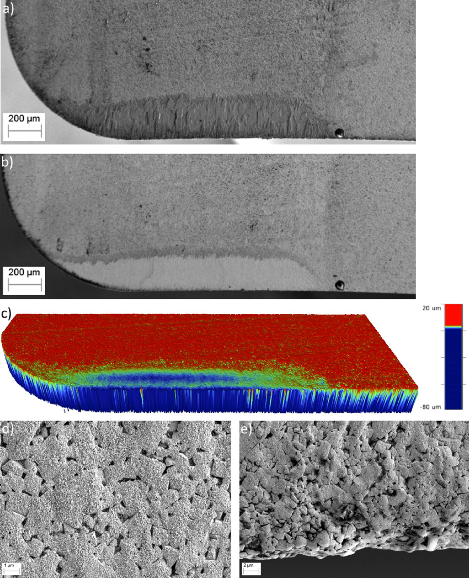
The small-scale surface roughness observed on all WC grains in the crater was analysed using AFM, exemplified in Figure 10. The features were typically protruding about 20 nm and were 50 nm wide. (However, since the features are packed closely together, they might be sharper than measured.) The pits between the WC grains, observed in the crater after etching, were confirmed to be 200–300 nm deep.
MN100 after test, etched in HF, measured by AFM. (a) 10 × 10 µm visualizing the pits between WC grains, (b) 1 × 1 µm visualizing the nano-topography on top of the centre grain in (a).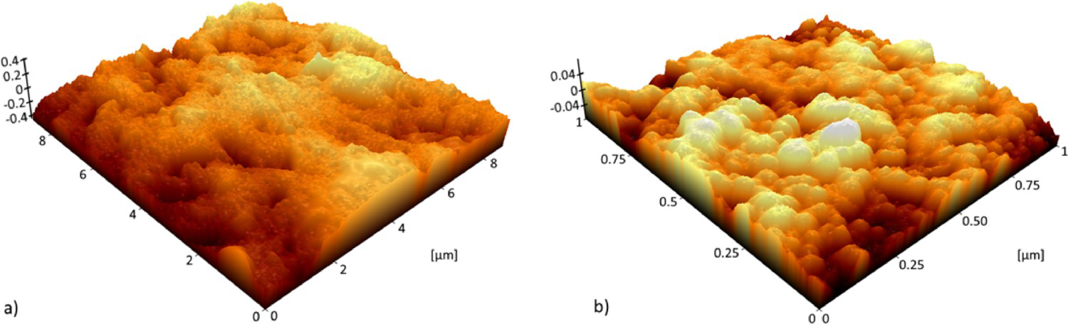
To study the influence from cutting speed on wear, cutting tests were repeated using a significantly lower as well as higher speed, but otherwise the same settings. The low-speed sample showed occasional transfer of titanium alloy and not as a smooth layer, along with part of a chip adhered to the cutting edge (see Figure 11). The high-speed sample, imaged in Figure 12, showed a smooth transfer layer, with large chunks of titanium alloy close to the cutting edge and along the transition area, similar to what was observed on the medium speed sample. Besides, some areas close to the transition area also showed pores in the otherwise smooth transfer film, exemplified in Figure 12(b).
LN200 after test. (a) Overview, (b) detail of transferred titanium in (a), (c) overview after subsequent etching, (d) detail of (c) in an area previously covered by transferred titanium (SEM, 3 kV) and (e) white light interference profilometry measurement of the area imaged in (c). HN200 after test. (a) Overview, (b) detail of transferred titanium indicated in (a), (c) overview after subsequent etching, (d) detail of crack in bottom of the crater indicated in (c) (SEM, 3 kV) and (e) white light interference profilometry measurement of the area imaged in (c).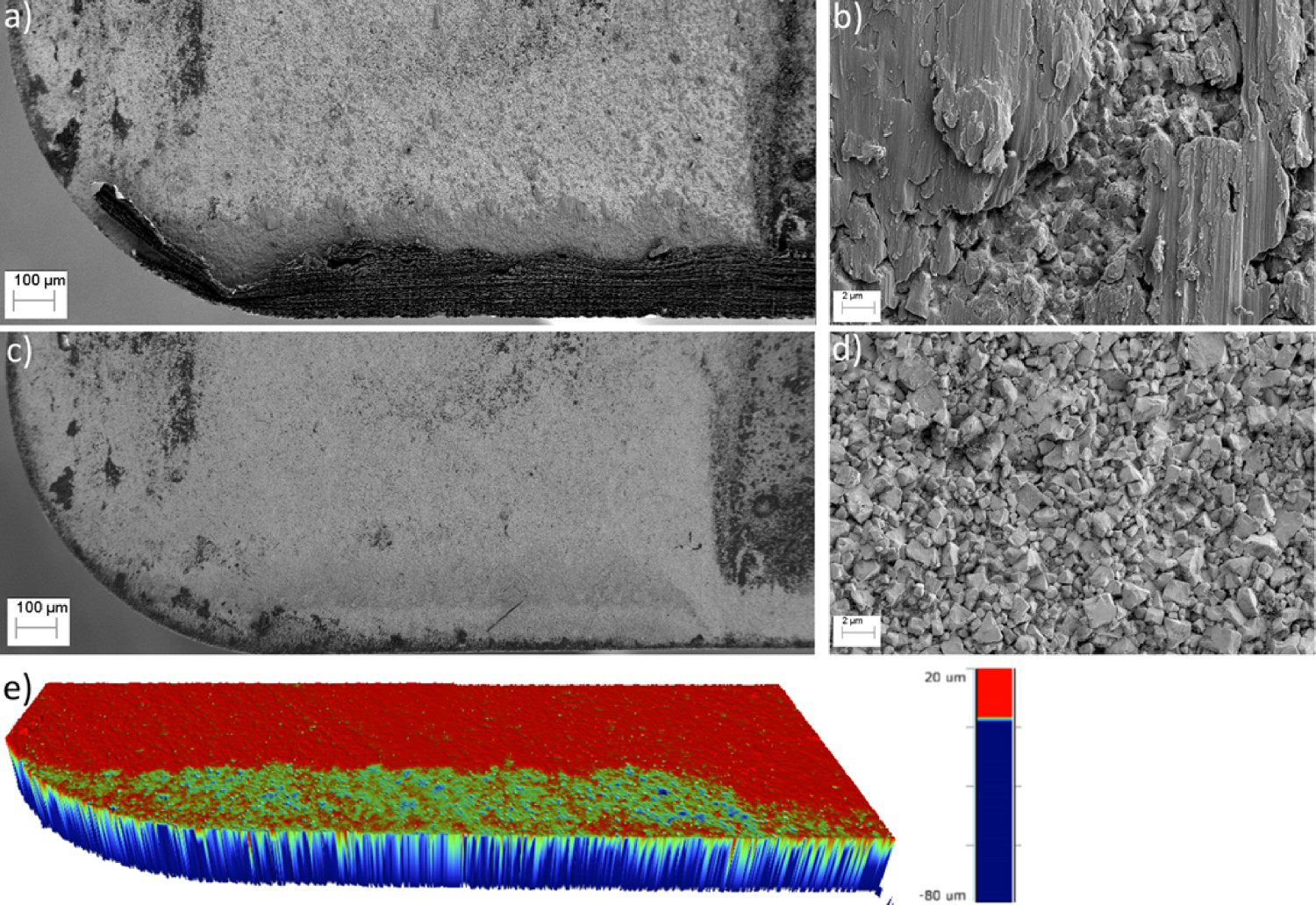
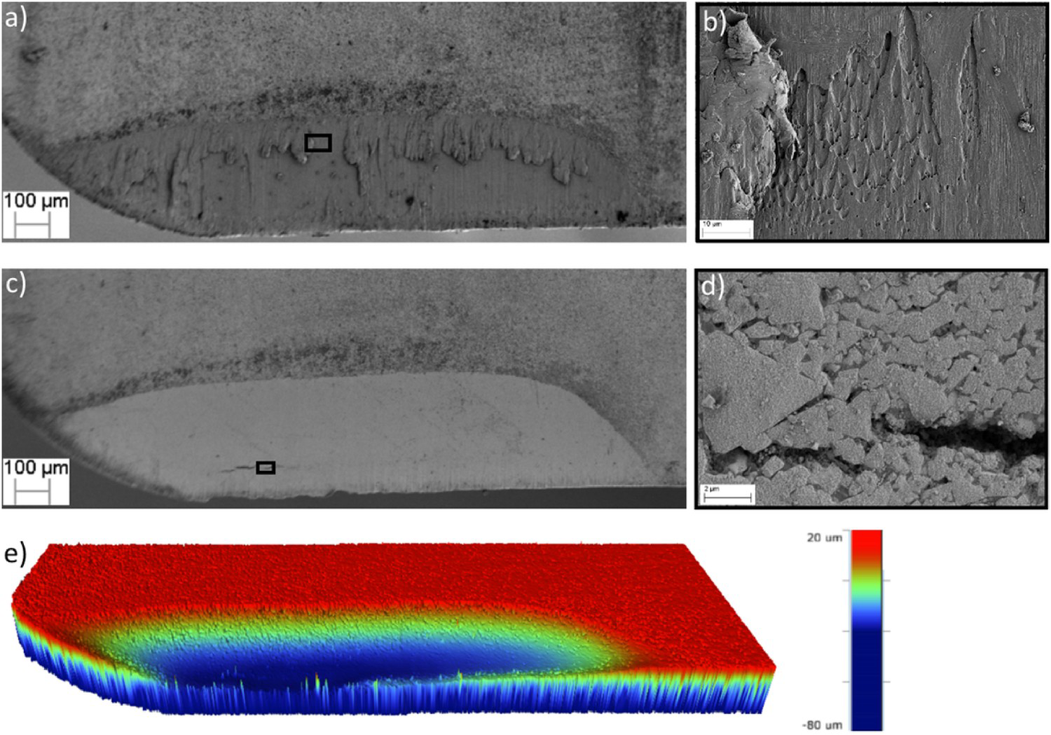
Both low- and high-speed samples were studied again after removing the titanium alloy using HF etching. The lower speed neither resulted in crater wear nor in carbon depletion after the 200 m sliding. Although there is a rough appearance in the high magnification image in Figure 11(d), the surface showed a very mild smoothening in the affected area, see Figure 11(e). The higher speed, on the other hand, resulted in critical crater wear with carbon depletion (confirmed by EDS, data not shown here); see Figure 12(c). The crater depth was 40 µm, much deeper than at medium speed, and cracking occurred along the cutting edge in the formed crater. The contact length also differs between the different speeds, indicated by the area appearing bright in SEM extending 120 and 350 µm from the cutting edge, respectively.
In cross-section, the medium- and high-speed samples appeared very similar, however, the titanium transfer was thinner with the higher speed (less than 1 µm, which is half of that measured in Figure 8), while the low-speed sample had clearly different appearance, see Figures 13 and 14. The high-speed sample showed nano-roughness on the WC grains and collection of titanium and carbon, including brighter WC grain fragments, in between these grains. The low-speed sample instead showed porous rough titanium transfer and loosening of single WC grains, clearly visible in higher magnification; see Figures 13(b) and 14(a).
Combination of top view and cross-section performed by FIB. (a) LN200, (b) detail of (a), (c) HN200 and (d) detail of (c). The light grey layers on top of the adhered Ti in (b) and (d) are platinum, deposited in situ in the FIB to protect the surfaces during cross-sectioning (SEM, 3 kV). Detailed images of the Ti/WC-Co interface. Cross-sections performed by FIB. (a) LN200, (b) MN200 and (c) HN200. The light grey layers on top of the adhered Ti in (a) and (c) are platinum, deposited in situ in the FIB to protect the surfaces during cross-sectioning (SEM, 3 kV).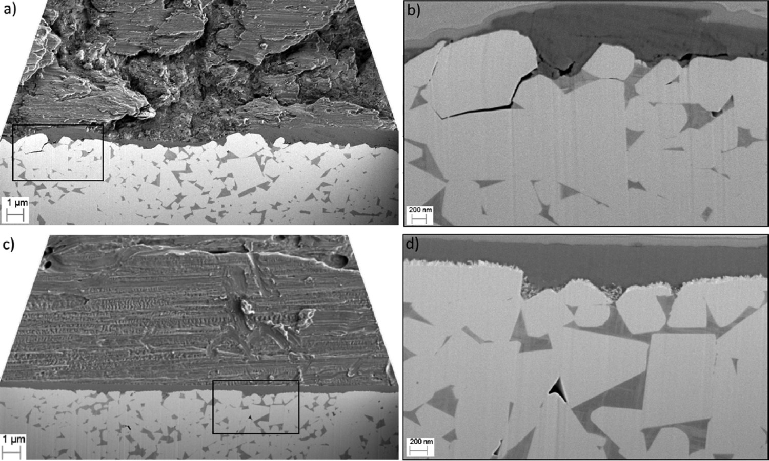
To evaluate the influence from feed on wear, tests were performed using a higher feed and a cutting length of 100 m. Severe wear of the cutting edge and cracking of the same was observed, after etching away the adhered titanium alloy layer and adhered chip (see Figure 15). Both the contact length and the crater depth were also increased, compared to normal feed, indicated by a crater extending about 430 µm from the cutting edge and with a maximum wear depth of 22 µm measured on the etched sample.
MH100 after test. (a) overview, (b) overview after subsequent etching, (c) white light interference profilometry corresponding to the area imaged in (b), (d) cutting edge with cracks (indicated with arrows), (e) bottom of crater (a-b, d-e SEM, 3 kV).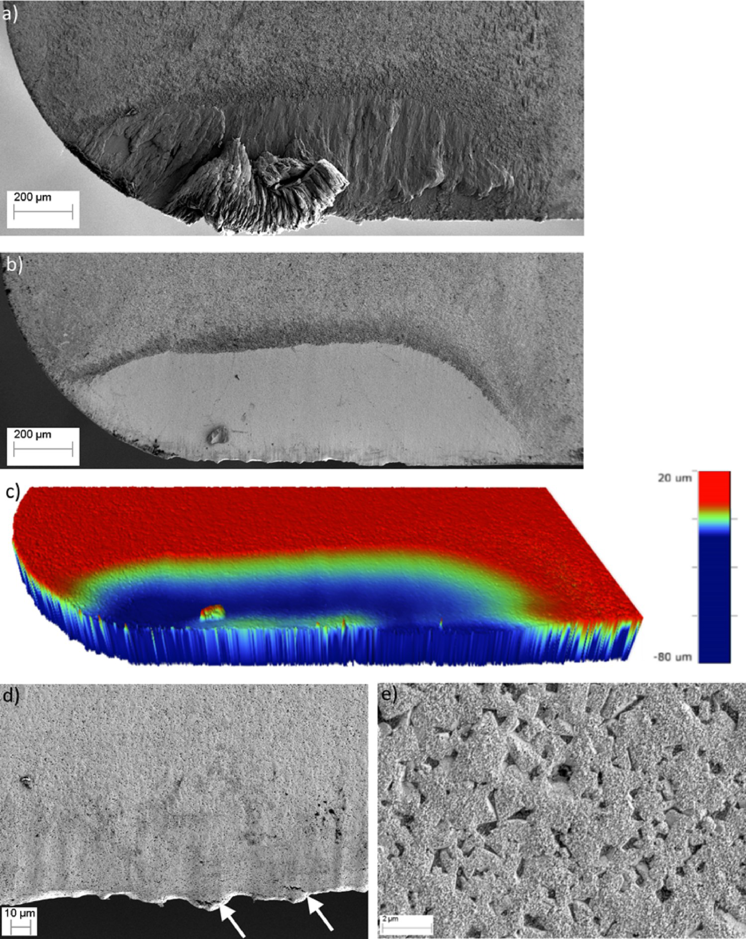
Influence from cutting parameters on wear
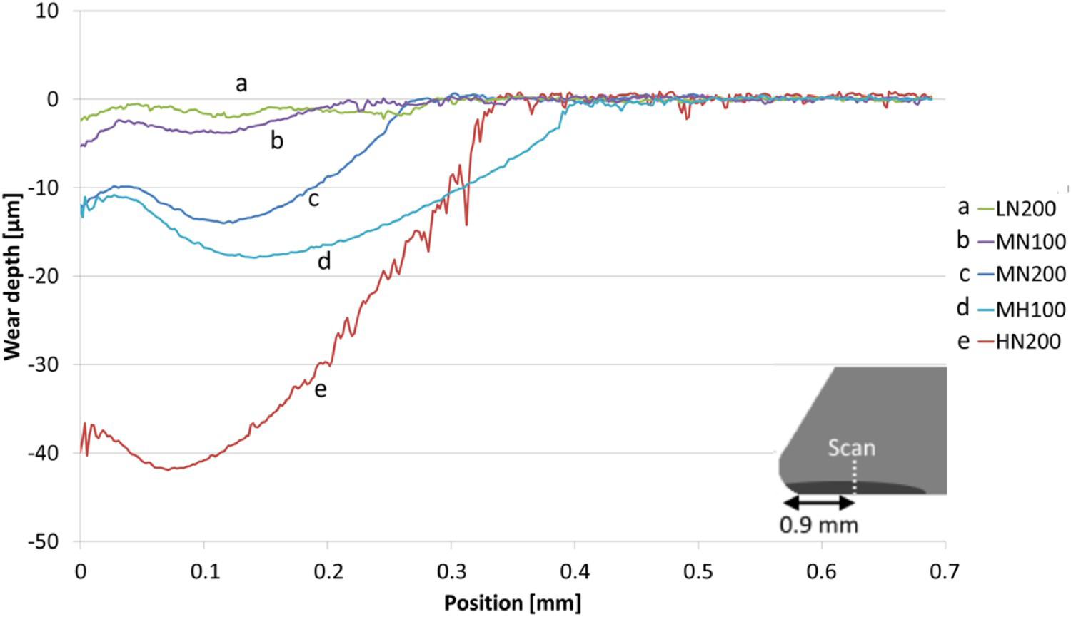
Crater wear is highly influenced by cutting length, cutting speed and feed, as previously reported in the literature [1,4,8–11,13]. Mapping the crater wear profile of the cutting inserts from all cutting tests in the same diagram, reported in Figure 16, the following is observed:
Neither low speed nor short cutting lengths result in high wear. Increased cutting length, speed or feed drastically increase the wear. In these tests:
○ Doubling the cutting length more than triples the wear depth (MN100 vs. MN200). ○ An increase in speed (by 40%) increases the final contact length and triples the wear depth (MN200 vs. HN200). ○ Doubling the feed increases the final contact length and the wear is more than quadrupled (MN100 vs. MH100). The location of the most severe wear is influenced as well and is not only explained by the change in final contact length. Medium speed and normal feed positions the deepest crater at about 120 µm from the cutting edge, while an increase in feed moves it further from the edge to 140 µm. An increase in speed instead moves it towards the edge to 70 µm. The location of the most severe wear on the rake face should be associated with the location of the highest temperature, i.e. not only the absolute temperature but also the temperature profile over the cutting edge is associated to the cutting parameters. Surface profiles of cutting inserts after testing and subsequent etching using HF. Each profile is acquired along a line perpendicular to the cutting edge, at the same position of all inserts (0.9 mm from the nose, as illustrated in the sketch).
Based on these data, a low cutting speed should be chosen to avoid crater wear. However, as mentioned in the introduction, the trend is rather to increase the cutting speed to increase productivity. In Figure 17, the removal rate of titanium is correlated to the absolute wear of the cutting insert (this is not to be considered a crater wear rate, since it changes during the test, compare MN100 and MN200). It is observed that a high cutting speed is more detrimental than a high feed for crater wear (compare HN200 and NH100, which have removed the same volume of titanium alloy from the work material cylinder). Thus, it indicates that a higher productivity is achieved more successfully by increasing the feed. However, other important parameters, like the surface integrity of the cut titanium surface, will also be affected and have a great influence on the choice of suitable cutting parameters.
The rate at which titanium is removed correlated to measured wear depth of the cemented carbide, after etching.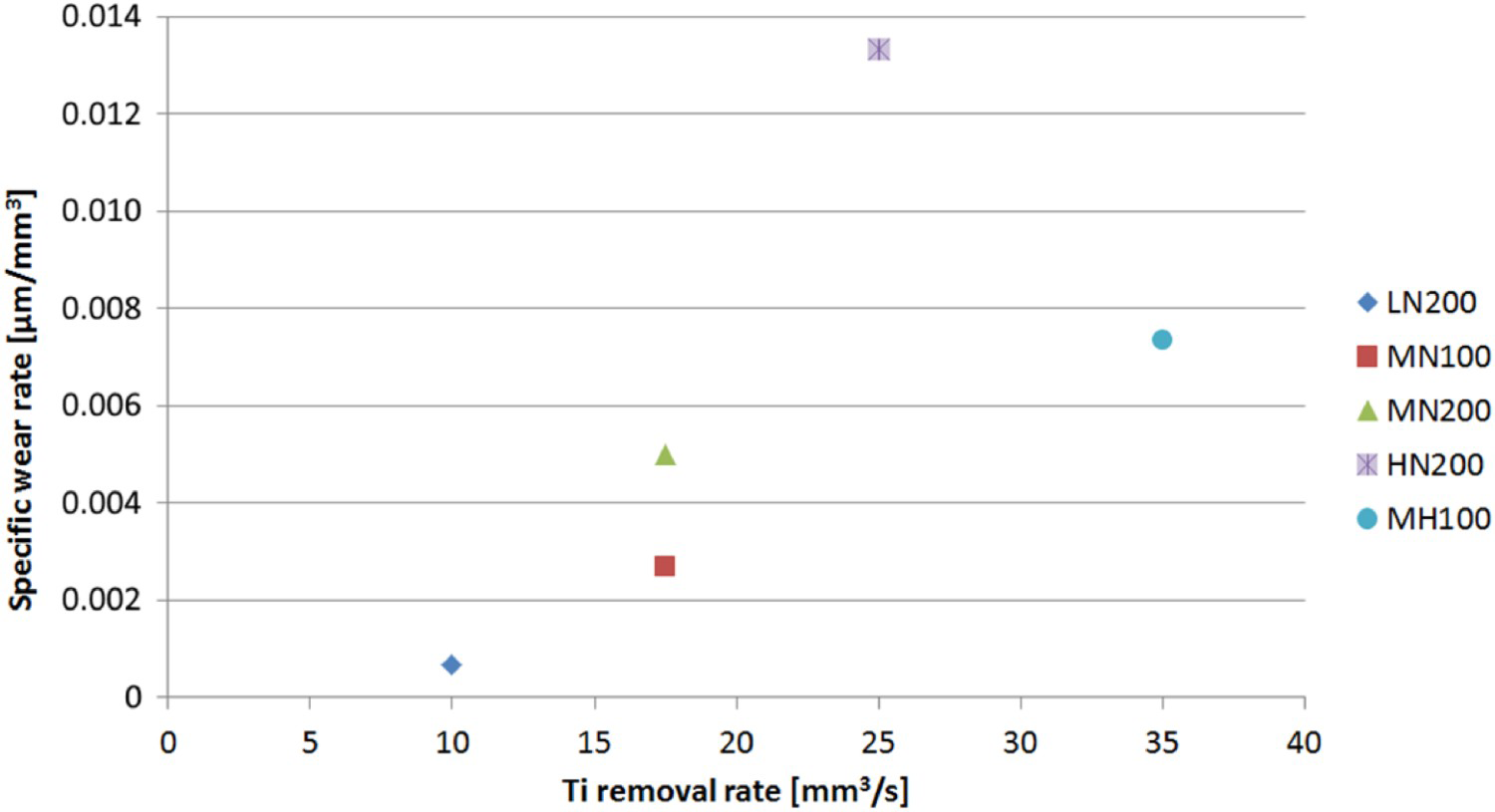
When the temperature is relatively low due to low cutting speeds, no crater is formed and no carbon depletion of the WC grains occurs. The surface is, however, slowly worn by the removal of protruding grains from the initially quite rough surface, as indicated in Figure 13(b). No gradual wear of WC grains can be observed in the cross-section. Hence, a certain speed, or rather a certain temperature, needs to be reached for the mechanisms leading to crater wear to become active (as observed also in [3,20]). The difference in wear mechanism at low cutting speeds is also strengthened by the lack of intimacy between transferred titanium alloy and cemented carbide, as indicated by the pores observed in the cross-section.
When the temperature is high enough that a crater is formed, the surface appearance is very similar irrespective of crater size and cutting parameters. After testing, the contact surface is covered by titanium alloy all the way from the cutting edge to the transition region, where the chip separates from the insert. The transferred layer is smooth; however, larger chunks of titanium alloy are found along the transition region. These seem to be very loosely attached to the underlying transfer layer, almost detached in some areas. It seems reasonable to think that these larger and loosely attached chunks are occasionally exchanged (removed and rebuilt). However, such large particles were not found on the corresponding chips. The particles found there were very small in comparison, only a few tens of microns, corresponding to small fragments of these presumably larger chunks. This could be explained either by successive removal of the large chunks or by their infrequent occurrence on the chip. Very long chips are generated for each test and only a small fraction has been investigated in the SEM.
The micrometre thick, smooth transfer layer effectively covers the cemented carbide insert and hinders direct contact between the cemented carbide insert and the newly formed chip. However, knowing that the crater grows deeper with increasing cutting length, it cannot be a static transfer layer. Either the transfer layer is gradually exchanged to allow for wear of the cemented carbide underneath or the crater grows only by diffusion wear.
After removing the transferred titanium alloy by etching, the craters show a very smooth, gradually worn cemented carbide surface. There are no traces of whole WC grains being removed. The surface is instead characterized by carbon-depleted WC grains, each with a nano-rough and tungsten-rich top surface, separated by shallow pits, as reported also in [16,20]. There is no indication of a fully covering TiC layer; however, in the pits between the WC grains, titanium and carbon are found. The cobalt, originally separating the WC grains, is located only further down. The shallow pits are not traces from the original surface preparation, since they are present also when several micrometres have been removed. This indicates that cobalt has been preferentially removed over WC. Since the wear continues with similar characteristics, it has to be gradual wear also of cobalt. For cobalt to be removed, also the titanium and carbon covering the cobalt have to be occasionally removed, separately or together with WC fragments and/or cobalt.
Conclusions
Low cutting speeds result in low wear, characterized by the occasional removal of whole WC grains and transfer of small particles of titanium alloy. Higher cutting speeds result in crater wear of the rake face. The crater wear is not proportional to the cutting length, speed and/or feed but accelerated with an increase in any of the mentioned parameters. If crater wear has occurred, it is covered by a smooth layer of transferred titanium alloy after testing. Underneath this transfer layer, the wear surface is smooth, with gradually worn WC grains. No traces of detached whole grains can be found. The gradually worn WC grains have become depleted of carbon and a thin tungsten-rich layer is found on top of each grain. This thin layer has a roughness in the range of tens of nanometres. The cobalt binder is preferentially removed, leaving shallow pits with titanium enriched in carbon in the top surface.
Footnotes
Acknowledgement
The authors would like to thank Stina Odelros and Susanne Norgren at Sandvik Coromant for valuable input and for providing the cutting inserts. Ernesto Vargas Catalán at Uppsala University is gratefully acknowledged for performing the etching.
Disclosure statement
No potential conflict of interest was reported by the author(s).