
Abstract
Electrochemical surface-enhanced Raman spectroscopy (E-SERS) is a powerful technique for the detection of trace levels of analytes in solution. It has wide ranging applications with a particular focus on biomarker detection. To perform E-SERS, nanostructured plasmonic metal electrodes are needed. Currently, a variety of fabrication methods are employed. This review defines the requirements for E-SERS electrodes and then describes and evaluates the current fabrication methods. The limitations of these techniques are discussed with the balance between ease of manufacture and magnitude of enhancement being identified as the key issue. Finally, suggestions for future areas of research are presented.
Keywords
Introduction
For the vast majority of diseases, early detection and diagnosis can lead to better treatment and improved quality of life [1,2]. Many of these illnesses can be identified by detecting specific molecules found in bodily fluids such as blood, urine or saliva, called biomarkers [3]. Biomarkers can include proteins, DNAs, RNAs, lipids and metabolites [4–6]. Therefore, there is a need for sensitive, selective chemical sensors which can detect biomarkers quickly and cheaply.
Effective sensors do already exist for certain conditions, such as the HIV antibody test and the preeclampsia urine test, but most are not sensitive or specific enough. Analytical methods, such as liquid chromatography-mass spectrometry and high-performance liquid chromatography, can achieve low detection limits but are time consuming and require expensive lab-based equipment [7].
In recent years, research has focussed on developing rapid, cost-effective point-of-care sensors. Some of the key areas of focus have been electrochemical (EC) biosensors [8–10], lateral flow assays [2,11], fluorescence-based optical biosensors [12–14] and gravimetric biosensors [15,16]. However, achieving the required levels of sensitivity and specificity simultaneously is often very difficult [17]. Surface-enhanced Raman spectroscopy (SERS) has been heralded as a technique which could overcome these limitations [18]. Despite this, it is still yet to achieve clinical use. Electrochemical SERS (E-SERS) is a type of SERS which combines electrochemistry and conventional SERS, which has the potential to reliably detect very low (<µM) concentrations of a biomarker in a complex biological liquid.
Principles of SERS
Raman spectroscopy is an analytical technique typically used to determine the vibrational and rotational states of a molecular system [19]. It provides a ‘structural fingerprint’ of a molecule by detecting the small fraction of light (approximately 1 in 107 photons) which is inelastically scattered [20]. Raman spectroscopy can be used to study a wide range of materials, but it is not sensitive enough to detect biomarkers in bodily fluids due to the weak Raman scattering.
SERS is a type of Raman spectroscopy in which the signal is enhanced (by factors of up to 108) due to the adsorption of the target molecule onto a nanostructured metal surface [18]. SERS was discovered in 1974 by Fleischmann et al. when an unexpectedly large Raman signal was observed while studying pyridine on an electrochemically roughened silver electrode [21]. This was the start of a lengthy debate into the reason for the SERS enhancement which has only recently reached a good agreement among researchers. It is now understood to be a combination of an electromagnetic (EM) and a chemical enhancement [18,22,23].
The EM enhancement is the result of an increase in the local EM field at the surface of the metal caused by local surface plasmon resonance (LSPR) [18,23,24]. LSPR is the resonant oscillation of free electrons confined within a metal nanoparticle (NP) caused by light with a wavelength that is less than or equal to the diameter of the particle (Figure 1) [25,26].
A schematic diagram illustrating LSPR.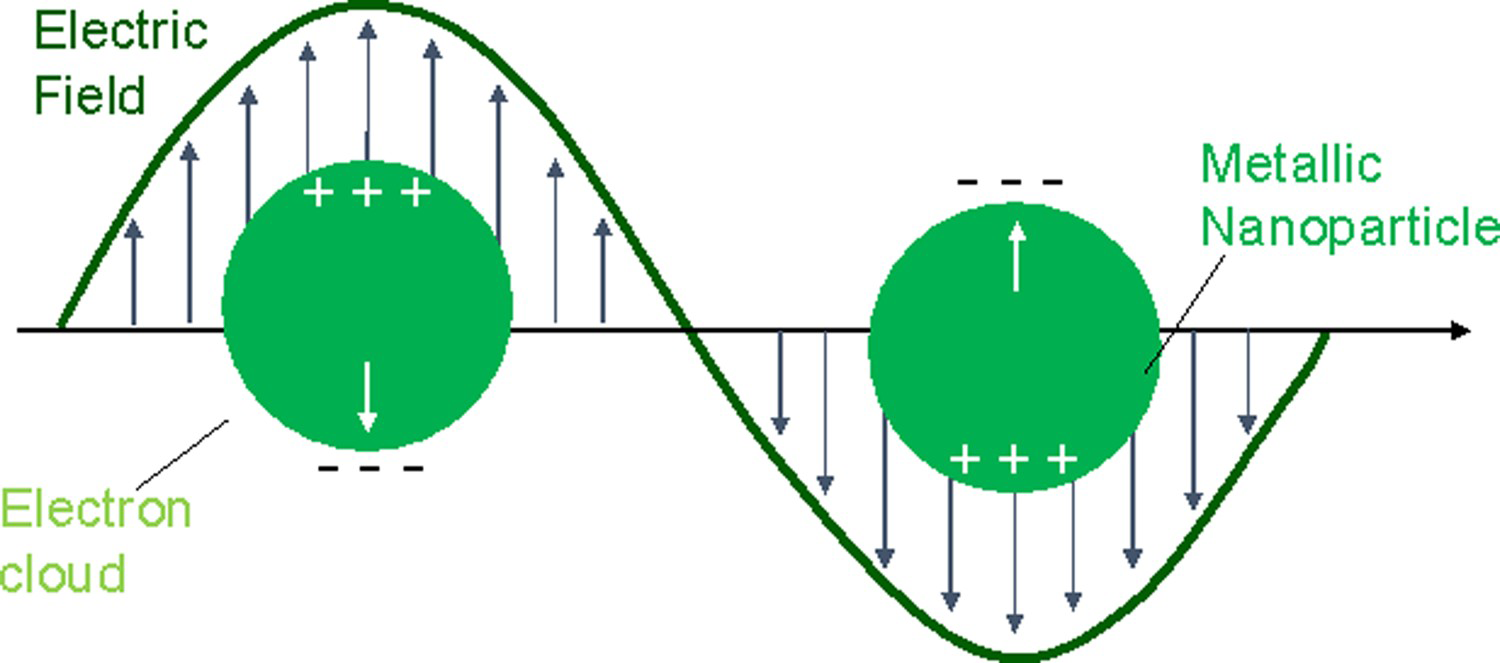
The EM SERS enhancement factor (EF) is generally approximated using the following relationship [18,23,24]:
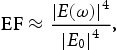
This relationship means that small changes in the local electric field have a substantial impact on the SERS signal [27]. The magnitude of the EM field depends on the size and shape of the NP [26]. Very large enhancements, known as ‘hot spots’, can be formed between two NPs or in carefully designed nanostructures [24,28–30]. Single particles do not exhibit particularly significant EFs (∼103) but very large EFs (∼105 to 108) are found at the junctions between two particles (Figure 2a). These enhancements decrease as the distance between the NPs increases. The greatest EFs have been calculated to occur when the separation between NPs is 1 nm [23,26–28]. Below 1 nm, quantum effects, such as electron tunnelling, are predicted to significantly reduce the field enhancement [31].
(a) The magnitude of the EM enhancement for dimers of silver NPs (left and middle columns) compared with single isolated silver NPs (right column). Reproduced from Ref. [28] with permission. Copyright 2000 American Chemical Society. (b) and (c) EM enhancements for a (b) spherical and (c) spheroidal gold NP. Adapted from Ref. [32] with permission. Copyright 2022 Royal Society of Chemistry.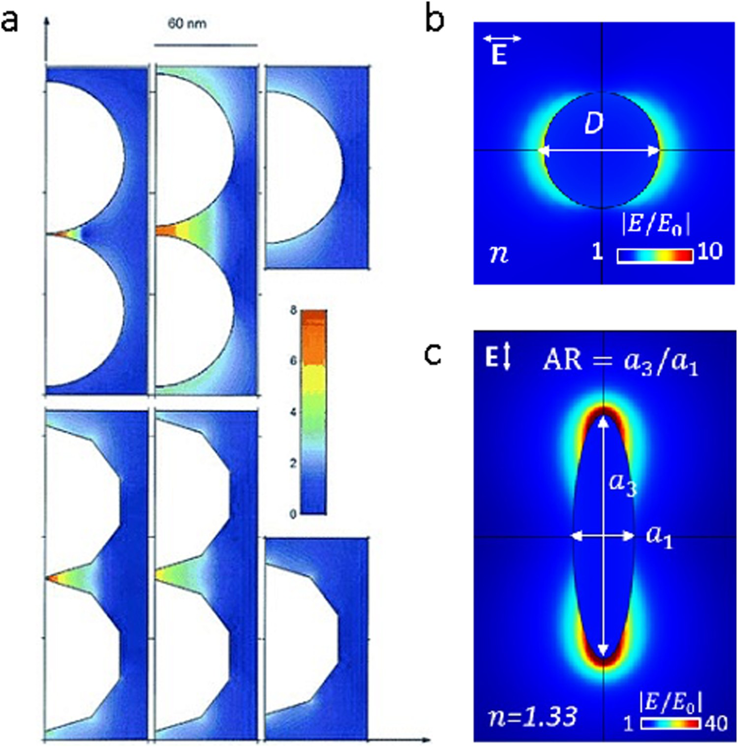
As well as at gaps between NPs, enhanced local electric fields are also found at sharp tips or edges of particles [33]. This is illustrated in Figure 2(b,c) where the EM enhancement is calculated to be significantly higher at the points of a spheroidal Au nanorod than around a spherical Au NP. The maximum EM enhancement at the points of an ellipsoid have been shown to increase with aspect ratio [32,34]. This has led to extensive research into non-spherical NPs for SERS such as nanorods, nanocubes, nanotriangles, nanostars and nanoflowers (NFs) [18,22,35–37]. Combining the enhancement from tips or edges with the ‘hot spots’ formed between particles can lead to enormous EM enhancements. For example, two triangular prisms positioned ‘tip-to-tip’ can exhibit enhancements of over 50,000 times the applied field [34].
The chemical enhancement of the SERS signal is much less significant than the EM enhancement but is notable because it can explain shifts in the Raman peaks [23]. The chemical enhancement is due to the adsorbed molecules transferring electrons to or from the metal, in either the ground or excited state, which can result in a change in the polarizability of the molecule. This can lead to a shift or increase in the Raman scattering signal [18,23,24].
Principles of E-SERS
E-SERS is a specific type of SERS which takes place within an EC cell [22,38]. As with a conventional EC cell [39,40], the system contains a working electrode (WE), reference electrode (RE) and counter electrode (CE) and an electrolyte but in E-SERS, the WE is a nanostructured metal surface which can also be used for SERS measurements (Figure 3) [22,38]. A potentiostat is used to control the potential of the WE [22].
Schematic diagram of the E-SERS system. SERS spectra are recorded using a three-electrode EC cell containing a WE, RE and CE.
Initially, E-SERS was simply seen as a method of studying EC reactions in situ using Raman spectroscopy [41]. However, it was later found that applying a potential to the WE could actually enhance the SERS signal [22,38]. There are three main reasons for this enhancement.
The first relates to the EC adsorption of analytes on the nanostructured surface. When a charged electrode is in contact with an electrolyte, an interfacial region, known as the EC double layer, will form between the surface and the bulk solution [39]. The nature of this double layer varies depending on the electrode potential. For example, if the electrode potential is more negative than the potential of zero charge, cations will be attracted to the surface and polar molecules such as water will interact with the electrode via their positively charged end [22]. The opposite is true for positive potentials. Consequently, the coverage, adsorption orientation and interaction strength of a target molecule at an electrode can be controlled using the potential [22,42–44]. This is significant because SERS is a surface-selective effect [24] and the magnitude of the SERS signal depends on the proximity of a molecule to the surface [26]. Therefore, increasing the adsorption of a target molecule on the surface will increase its SERS signal.
The second reason for the E-SERS enhancement relates to the number of electrons at the metal surface. Changing the potential of the electrode alters the surface charge density in the plasmonic nanostructure [22]. The surface charge density controls the frequency and amplitude of the surface plasmon resonance which is the reason for the EM SERS enhancement. When a negative potential is applied to the electrode, more electrons are injected into the SERS substrate, increasing the magnitude of the LSPR and consequently the magnitude of the SERS signal.
The third reason is linked to the Fermi level of the metal. The Fermi level determines the likelihood of photon-driven charge transfer between the electrode and the adsorbed molecules [22]. Charge transfer processes play an important part in the chemical enhancement of the SERS signal. Changing the potential of the electrode alters the Fermi level of the metal which can increase the probability of charge transfer between the electrode and the adsorbed molecules [44,45]. An increase in charge transfer processes can lead to an enhancement in the SERS signal.
The relative importance of these three phenomena depends on the system. The structure and composition of the electrode, the analyte, the electrolyte and the environment all affect the E-SERS enhancement. Consequently, it can be difficult to establish the factors at play. Much of the research which has helped to illuminate this subject has been performed on very simple or well-studied analytes such as water and rhodamine 6G [46,47].
The interest in E-SERS is not simply due to the increased SERS signal. It is a powerful technique because it can control which species adsorb onto the surface and how their SERS signal is enhanced. This could enable multiplexing through the detection of different molecules at different potentials. Therefore, increasing the possibility of using SERS to detect biomarkers in complex biological fluids.
Review methodology
The aim of this review is to evaluate the nanostructured electrodes (NSEs) that have been used for E-SERS and identify the most promising approaches. The NSE is a critical part of the E-SERS system because it determines the magnitude of the Raman signal enhancement. Since the 1970s, there have been thousands of papers on the fabrication of nanostructures for SERS which have been extensively reviewed [18,24,26,48–51]. To avoid repetition, this review will focus on NSEs that have been used for E-SERS and will only highlight SERS nanostructures that have the potential to significantly advance E-SERS research.
Requirements for E-SERS NSEs
Before evaluating the literature, it is useful to identify the requirements for an E-SERS NSE. One of the most important features of E-SERS is that the same set-up can be used for EC measurements [39,52] (e.g. cyclic voltammetry and square-wave voltammetry), conventional SERS and E-SERS (SERS with an applied potential). This multipurpose system can therefore extract a lot of useful data and enables sophisticated chemical analysis. However, this also means that the NSE must be suitable for all of these methods. The key features of an E-SERS NSE are as follows:
Plasmonic resonance in the visible/near-infrared range (∼400 to 1000 nm) [26]. Generally, this is the case when the real part of the dielectric function (Re(ϵ)) is negative and the imaginary part (Im(ϵ)) is small [48]. Gold, silver and copper all fulfil these criteria [48]. EC stability. This is why gold is a very popular NSE material [24,48]. Feature size that is less than ∼100 nm [26]. Particularly large EFs can be achieved when ‘hot spots’ are formed between two NPs or at sharp edges or tips [24]. A regular structure that can be reproducibly fabricated to give consistent results [24]. Large surface area to allow many molecules to adsorb onto the surface at once [26]. Fast electron transfer kinetics [40].
Using the EF or limit of detection to evaluate SERS substrates
Throughout this review, the SERS EF or lowest concentration of an analyte detected are quoted as a way of quantifying the performance of a substrate. Although these are the typical metrics used to evaluate SERS nanostructures, they should be treated with caution [26]. The SERS EF is determined experimentally by measuring the intensity of the SERS signal for an absorbed molecule on the metal surface, relative to the intensity of normal Raman signal of the same ‘free’ molecule in solution [24]. The two intensities must be normalised by the number of molecules either on the surface (SERS) or in the solution (conventional Raman) [24]. Issues arise due to difficulties in calculating the number of molecules on the surface and the fact that some researchers calculate the EF based on signals produced at ‘hot spots’ on the metal surface rather than the average signal across the substrate [26]. This can make it difficult to compare work because papers often do not contain details of how the EF is calculated.
Comparing the lowest concentration of an analyte detected can also cause problems because some molecules are much better Raman scatterers than others [26]. For example, dye molecules such as rhodamine 6G exhibit very large ‘resonant Raman scattering’, so being able to detect µM levels of these molecules is less significant than being able to detect the same concentrations of another non-resonant molecule.
The most effective way to evaluate a novel NSE is to perform SERS measurements for the new NSE and a traditional NSE in the same way, using the same analyte and equipment. This review has tried to include this information if it is available in the papers being reviewed.
NSEs
Electrochemically roughened electrodes
The first E-SERS measurements were performed using electrochemically roughened silver electrodes [21]. In this process, successive EC oxidation and reduction cycles are used to create a nanostructured metal surface [38,49]. Initially, a positive potential is applied to the electrode to form soluble ions or an insoluble surface complex, then a negative potential is used to reduce these species, resulting in a randomly, roughened metal surface (Figure 4) [38]. The established methods for electrochemically roughening gold, silver and platinum are described by Wu et al [22]. For gold electrodes, the procedure is as follows: first, the surface is cleaned electrochemically in 0.1 mol/L H2SO4 solution and rinsed with ultrapure water. The electrode is then placed in 0.1 mol/L KCl and held at −0.3 V until the current is stable. Next, the potential is scanned to 1.2 V at 1 V/s, set for 1.2 s to allow oxidation and then scanned back to −0.3 V at 0.5 V/s and set for 30 s to allow reduction. The cycle is repeated for at least 15 min to produce a roughened surface [22,53].
Scanning electron microscopy (SEM) images of electrochemically roughened Au films held at 1.2 V in 0.1 M KCl for different numbers of cycles: (a) 3 cycles, (b) 5 cycles and (c) 12 cycles. Adapted from Ref. [54] with permission. Copyright 2020 Elsevier.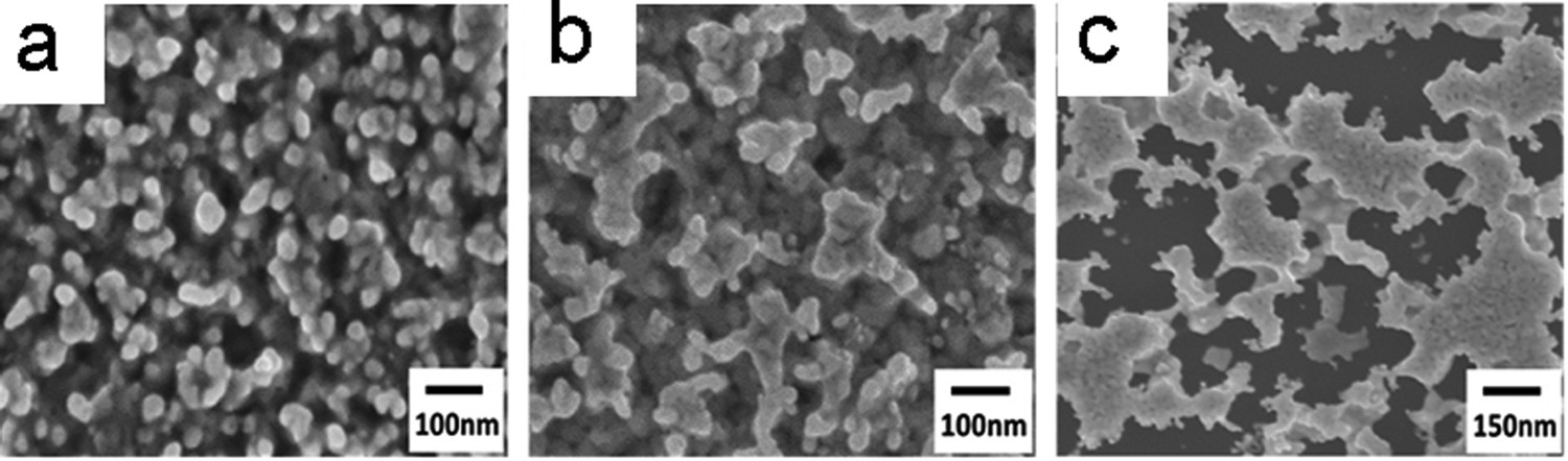
Despite their initial success, SERS research has moved away from electrochemically roughed electrodes since the early-2000s [22]. The structures are random and contain features from the angstrom to micron scale [49]. This means the SERS enhancement varies across the surface and between electrodes [38]. However, there are some recent examples of EC roughening being used as a quick, easy, in situ method of E-SERS substrate fabrication [55–58]. This approach is particularly suited to E-SERS because the same set-up can be used for surface preparation and analyte detection. Martín-Yerga et al. electrochemically activated silver screen-printed electrodes (SPEs) in situ whilst simultaneously performing E-SERS of a probe molecule [55]. They were able to quantitatively detect nM levels of ferricyanide and tris(bipyridine)ruthenium (II) [55].
Colloidal NPs deposited on rigid substrates
Colloidal NPs synthesised via wet chemistry are a staple of SERS [59–62]. Gold NPs can be cheaply and reproducibly synthesised using techniques such as the Turkevich–Frens method [59–61]. In this method, tetracholoauric acid (HAuCl4) is reduced by sodium citrate in water, with citrate also acting as an electrostatic stabiliser [59,60]. By carefully controlling the nucleation and growth steps, NPs with defined diameters between 10 and 200 nm ±10% can be synthesised [61]. Silver NPs can be synthesised using a similar citrate reduction of silver nitrate (AgNO3) [63].
Colloidal NPs can be used in E-SERS by drop-casting or spin coating them onto a rigid conductive electrode (e.g. glassy carbon, indium tin oxide (ITO) or gold). Compared to electrochemically roughened electrodes, the surface features are much more uniform in size and the surface signal difference across the whole surface can be less than 10% (Figure 5) [22]. This approach has been used successfully in a number of E-SERS sensors [46,64–73].
(a) SEM image of a multi-layered drop-cast Au/Ag NP electrode prepared on a SPE by Zhao et al. Inset: Schematic of the layered structure. (b) E-SERS spectra recorded using the multilayer Au/Ag electrode for 0.5 mM uric acid in 0.1 M NaF supporting electrolyte. Adapted from Ref. [67] with permission. Copyright 2015 American Chemical Society.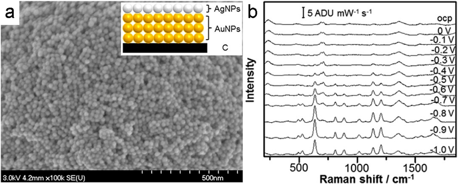
Goodall et al. developed an E-SERS system for the detection of uric acid in urine, an early indicator of preeclampsia in pregnant women [66]. They synthesised silver NPs using a standard citrate reduction (Lee and Meisel method [63]) and then drop-coated them onto a commercially available carbon SPE. The electrode was placed into an EC cell containing 1.0 mM of uric acid in urine simulant and the SERS signal was measured at potentials between 0 and −1 V. The most intense uric acid peaks were observed at −0.8 V vs. Ag/AgCl. At this potential, uric acid concentrations below 0.4 mM were easily identified [66]. Quantitative detection was not achieved in this work but two years later, the same group reported quantitative detection of uric acid at concentrations between 0.1 and 1 mM using a multi-layered Au/Ag NP electrode [67]. Although these detected concentrations are not particularly low compared to other SERS-based sensors, they are good enough to pass the threshold for a preeclampsia diagnostic test (0.4 mM of uric acid). This demonstrates that it is not always necessary to develop the most sensitive sensor possible but rather the most effective system for the application.
Spherical NPs are highly reproducible and cost-effective but only have moderate signal enhancement due to their high symmetry [18,32,74]. More advanced NP shapes which amplify the Raman signal through hotspots at tips and edges are the focus of intense research [18,24]. There are now many papers and reviews which discuss different NPs for SERS including nanorods, nanocubes, nanostars and NFs [18,22,35–37,75]. So far all of the published work on colloidal NPs in E-SERS has used spherical NPs. However, given the attention anisotropic particles have received in SERS research, it seems likely that E-SERS will also start to investigate non-spherical NPs to enhance the Raman signal.
The main problem with depositing colloidal NPs on rigid substrates is the non-uniform distribution of the particles on the surface which limits the SERS enhancement [22]. Some methods have been developed to arrange the NPs in a regular pattern [18,76,77]. Wang et al. produced highly ordered NP arrays with sub-10-nm gaps through the self-assembly of cetrimonium bromide (CTAB)-capped gold NPs (Figure 6) [76]. CTAB is a surfactant which forms a bilayer around the Au NP. This bilayer leads to a net positive charge on the NP surface which results in a repulsive force between the NPs that prevents aggregation. Empirical EFs above 1 × 10⁸ were observed for p-mercaptoaniline under near infrared (785 nm) excitation [76]. However, one of the issues with using CTAB-capped NPs is that it is necessary to remove some of the surfactant molecules to allow the analyte of interest to reach the NP surface [77]. More recently, Smith and Lipkowski fabricated a reproducible 2D array of Au NPs by coating gold NPs in SiO2, arranging them on a gold substrate, dissolving the SiO2 and then electrochemically cleaning the substrate [77]. This resulted in a monolayer of bare Au NPs with a regular spacing that was twice the SiO2 shell thickness (4.2 ± 0.7 nm) [77].
(a) Fabrication process used by Wang et al. to produce NP arrays through the self-assembly of CTAB-capped gold NPs. (b) SEM images of Au NP array. Adapted from Ref. [76] with permission. Copyright 2005 American Chemical Society.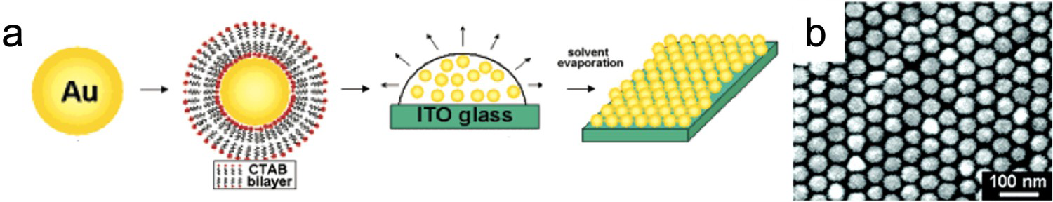
Electrochemical deposition of plasmonic metal NPs
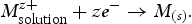
NSEs can also be fabricated via electrochemical deposition (ED) [78–89]. In this method, solid metal NPs are deposited onto a WE from a solution of ions through the application of a positive potential [90]. The reduction of the metal ions can be represented by
Like EC roughening, ED requires a three-electrode EC cell and a potentiostat [90]. This makes it an attractive fabrication process for E-SERS because it uses much of the same equipment. It also has the potential to be quicker and easier than using colloidal NPs because the NPs are deposited straight onto a rigid, conductive substrate, removing the need for drop-coating.
Dai and Compton first electrodeposited gold NPs onto ITO in 2006 [86]. They used 0.1 mM of HAuCl4 in 0.5 M H2SO4 as their electrolyte and applied a potential step from +1.055 V to −0.045 V (vs. saturated calomel electrode) for a fixed time (15, 50, 150 or 300 s). Varying the experimental parameters revealed (unsurprisingly) that the particle size increased with
Wang et al. refined Dai and Compton's method in 2013 using a two-step approach (Figure 7) [79]. First, they applied a potential step from +0.89 V to −0.8 V (vs. a saturated calomel electrode) to an ITO WE in a solution containing 0.1 mM HAlCl4 and 0.1 M NaClO4 for 10 s. This step triggers the formation of many small gold NPs (mean diameter of 9 ± 2 nm and particle density of 1800 ± 200 particles per µm2). These NPs then act as seeds in the subsequent growth step due to the preferential reduction and deposition of The two-step ED process used by Wang et al. to form gold NPs on ITO. Reproduced from Ref [79] with permission. Copyright 2013 American Chemical Society.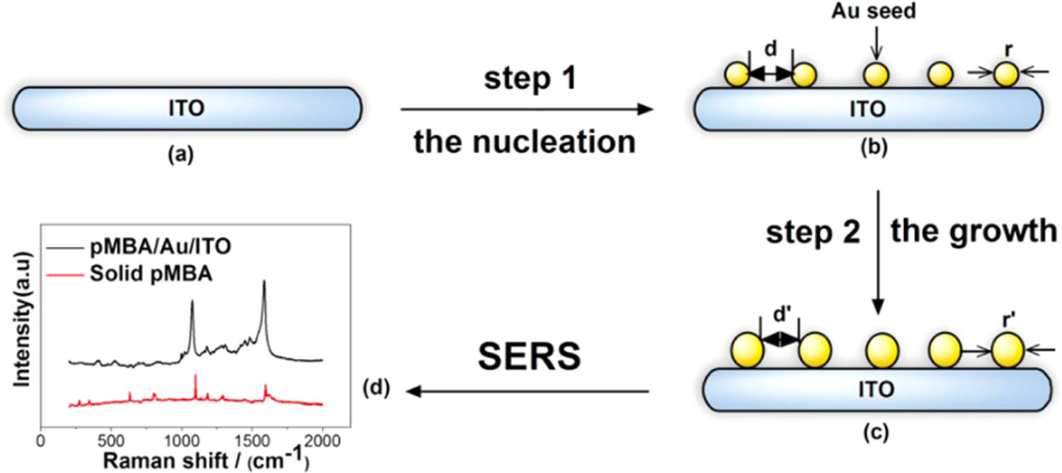
As discussed ealier, anisotropic NPs can display enhanced SERS signals due to ‘hot spots’ which form at edges or tips. The electrodeposited NPs discussed so far have all been spherical but there have been some attempts to ED non-spherical NPs [80,85,88,91–93]. Flower-like nanostructures (NFs) can display high SERS EFs due to the nanogaps that form between their ‘petals’ [80].
Ye et al. electrodeposited gold NFs onto ITO from a solution of 2 mM HAuCl4 and 0.1 M KNO3 at a constant potential of −0.1 V [80]. The ITO electrodes were coated with polydopamine (Pdop), a multifunctional biopolymer, which triggered the formation of Au NFs. The reason for the change in morphology is not completely clear but Ye et al. do show that the Pdop increases the nucleation rate of the gold NPs [80]. They studied the SERS response of the nanostructures using rhodamine 6G as a probe molecule and found that the Raman peaks were significantly larger for the NFs than the NPs [80].
NSEs fabricated using template-based methods
Despite being able to regulate the size of colloidal and electrochemically deposited NPs, it is still difficult to control the spaces between them [22]. This leads to variation in the SERS enhancement because ‘hot spots’ formed at the gaps between NPs play a vital role in signal amplification [24]. Template-based methods can be used to create very ordered NSEs with controlled inter-particle spacing [22]. The most popular template-based method in SERS research is nanosphere lithography (NSL) which was proposed by Hulteen and Van Duyne in 1995 [94]. This procedure is demonstrated in Figure 8. First, monodisperse polystyrene or SiO2 nanospheres with a chosen diameter are placed onto a substrate and allowed to self-assemble into a close-packed hexagonal array [95,96]. The substrate should be thoroughly cleaned, and, for E-SERS, it must also be conductive (e.g. ITO or metal coated glass) [22]. Next, a thin layer (15–100 nm) of metal is deposited by physical vapour deposition on top of the spheres [95]. The nanospheres are then washed away leaving a uniform triangular NP array on the surface.
The NSL fabrication process. Monodisperse nanospheres are deposited onto a substrate and allowed to self-assemble into a close-packed hexagonal array. Then, a thin layer of metal is deposited by physical vapour deposition on top of the spheres. The nanospheres are washed away leaving a uniform triangle NP array.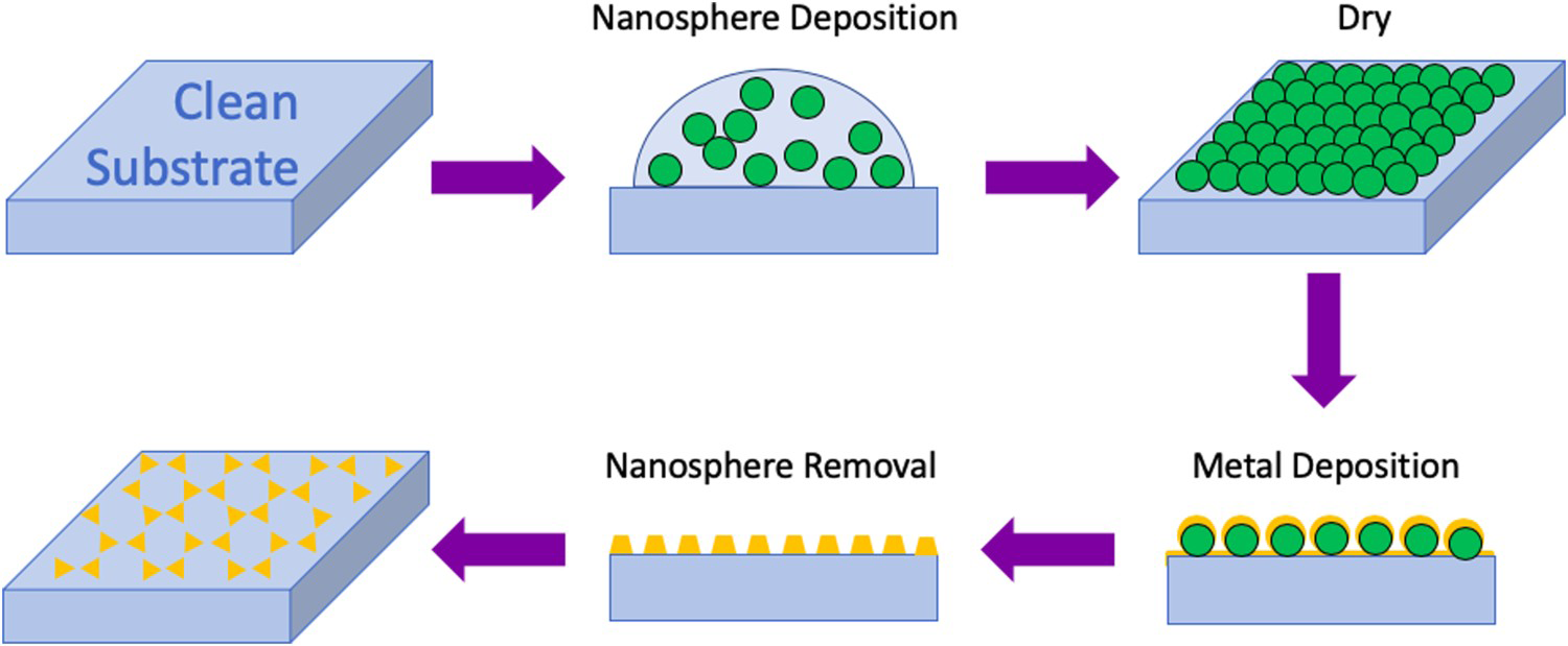
The basic NSL method described above can be modified in different ways to produce the desired nanostructured surface [97,98]. For example, Zhang et al. were able to modify the shape of NSL-fabricated silver triangles on ITO using EC oxidation [98]. A potential step from +200 mV to +400 mV was applied to the nanotriangles which selectively oxidised the triangles, first at the bottom edges, then at the tips and finally from the top face [98]. Applying multiple cycles resulted in a regular array of spherical NPs (Figure 9).
Ag NPs on ITO produced by Zhang et al. using NSL. (a) SEM images of Ag NP array produced using nanospheres with a 590-nm diameter. (b) The LSPR λmax of the Ag NPs shift towards shorter wavelengths after applying a potential step. Atomic force microscope images of a NP (c) before any EC measurements, (d) after one cycle and (e) after two cycles. Adapted from Ref. [98] with permission. Copyright 2005 American Chemical Society.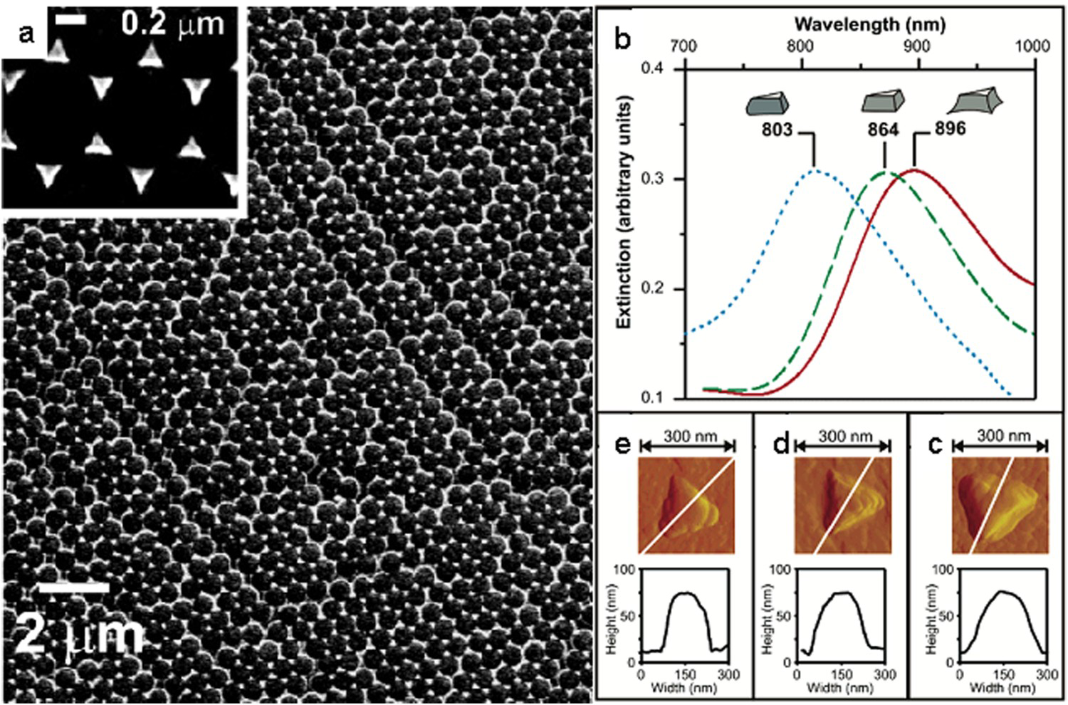
Van Duyne's group also developed another NSL method called ‘film over nanosphere’ (FON) [95,99,100]. In this method, a thicker metal layer (∼200 nm) is deposited on top of the polystyrene or SiO2 nanospheres and, unlike tradition NSL, they are not removed. This results in a very uniform rough surface [99]. Zhang et al. used silver FON electrodes to perform E-SERS measurements of pyridine and the Ru(bpy)3+/Ru(bpy)2+ complexes as well as dipicolinic acid (DPA), an anthrax bacterial endospore marker [101]. They were able to detect 8 × 10⁻⁵ M of DPA in 5 min [101]. This was a significant improvement on the results achieved using a traditional electrochemically roughened silver electrode. Despite the many benefits of NSL, the complexity of the process leads to several drawbacks. Physical vapour deposition requires expensive, specialist equipment and a significant amount of the deposited gold or silver is wasted when the nanospheres are washed away. The number of steps also makes the process quite time-consuming and costly.
In the early-2000s, Bartlett and his colleagues developed a version of NSL which did not rely on expensive, specialist vapour deposition equipment [102,103]. The sphere segment void (SSV) method uses the same hexagonal arrangement of uniform nanospheres but instead of depositing a metal film on top of the spheres, the metal is electrodeposited onto the substrate between the nanospheres [102,104]. Removing the spheres results in a thin structured film containing a regular hexagonal array of uniform voids [22,102]. The size of the voids can be controlled by varying the thickness of the film. Figure 10 shows a copper/silver SSV surface fabricated using 1 µm diameter spheres.
(a) SEM image of a polystyrene monolayer film used for the SSV method. (b) and (c) SEM images of the resulting Cu/Ag SSVs. Adapted from Ref. [105] with permission. Copyright 2019 American Chemical Society.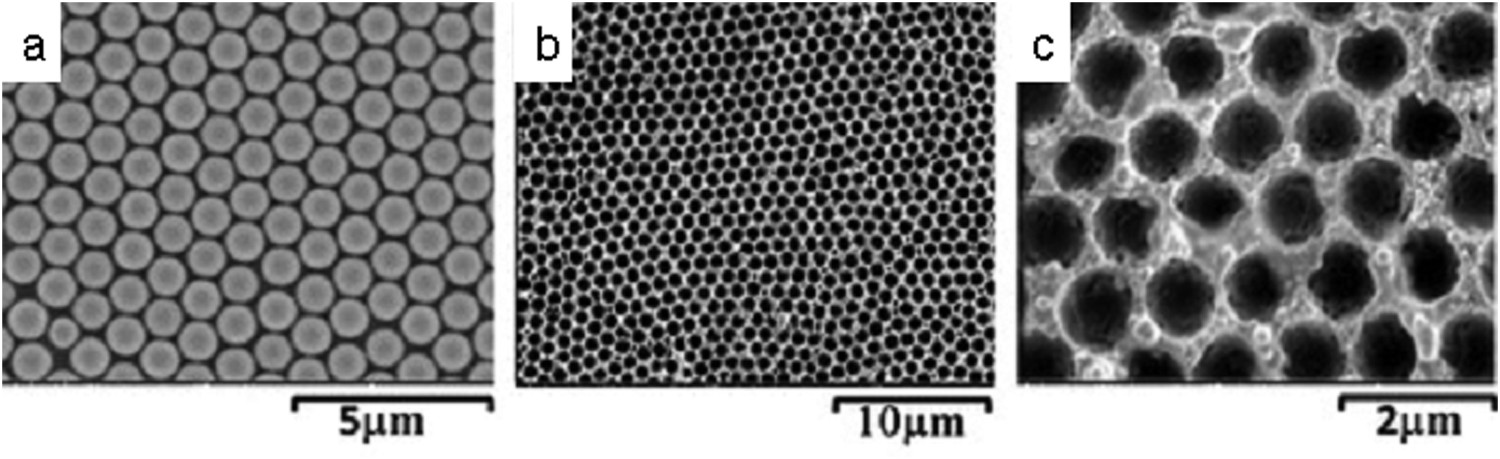
The SSV method is an attractive electrode fabrication technique for E-SERS because it uses the same equipment needed for the EC measurements. There have been a number of successful attempts to use SSV for E-SERS [104,106–108]. For example, Abdelsalam et al. fabricated SSV structured silver surfaces and used them to study the oxidation and reduction of a flavin analogue (isoalloxazine) [107]. The SSV surfaces gave stable, reproducible surface enhancements at a range of electrode potentials and the spectra were sensitive to sub-femtomole quantities of immobilised flavin [107]. SSV is cheaper than conventional NSL because it does not require expensive vacuum chambers and less metal is wasted during fabrication. However, it is still a time-consuming multi-step process which could mean it is unsuitable for use in commercial sensors.
Electron beam lithography is another technique that can be used to create NPs with precise sizes, shapes and spacings [95,109]. In this method, a substrate is coated with an electron sensitive polymer film (or resist) and then a focussed beam of electrons is used to draw custom shapes in the film [110,111]. The electron beam changes the solubility of the polymer allowing either the exposed or unexposed areas of the resist to be dissolved, resulting in a patterned mask. A metal film is then deposited on top of this mask and the polymer is washed away, leaving behind a nanostructured metal surface [95,110]. This method can create uniform nanostructures with dimensions below 10 nm but again, it is expensive and time-consuming [110,112]. The equipment required is even more expensive and specialist than that which is needed for NSL. As such, it is not practical to use this technique in industry, but it can be utilised in fundamental EC research [44,113].
Oyamada et al. fabricated well-defined gold dimer structures with a gap distance of 2.5 nm using electron beam lithography [44]. They used these nanostructures to conduct E-SERS measurements of two structural isomers, 4,4′-bipyridine (44bpy) and 2,2′-bipyridine (22bpy), at different applied potentials. They found that the Raman signals increased for both of the molecules at negative potentials. However, when they used a mixed solution of 44bpy and 22bpy, the signal for 44bpy was larger at positive potentials and the signal for 22bpy was larger at negative potentials, showing that the dominant absorbent could be controlled using the electrode potential [44]. This type of fundamental research helps to shed light on the complex EC interactions which take place at electrode surfaces [42].
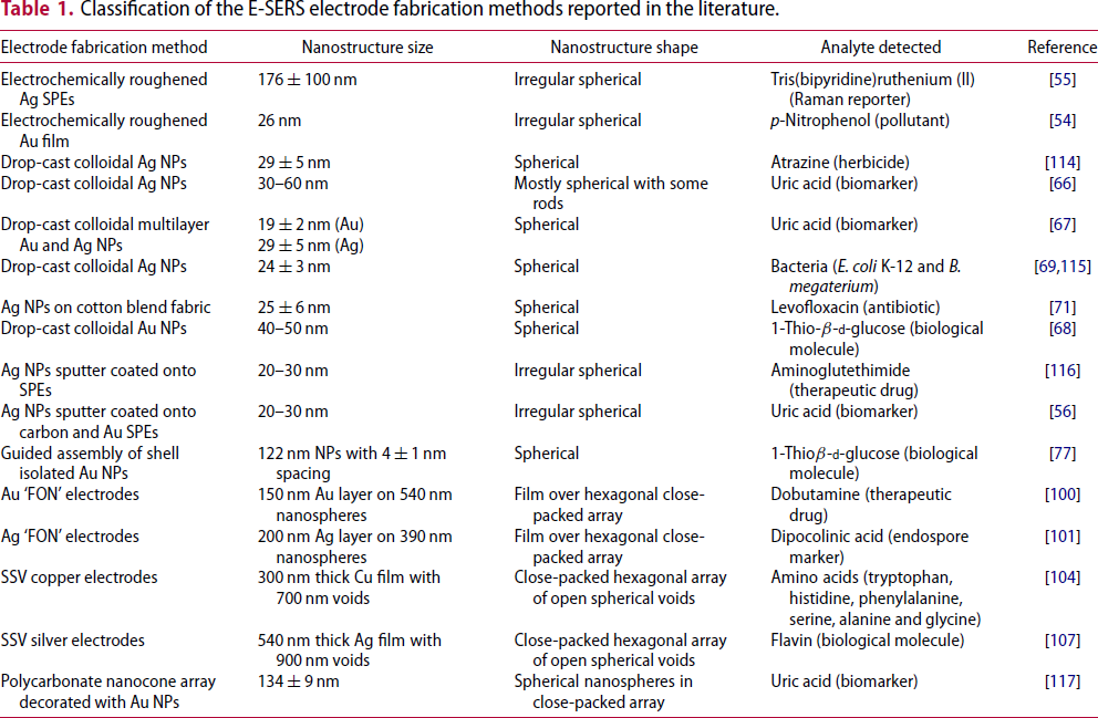
Classification of the E-SERS electrode fabrication methods reported in the literature.
Analyte detection with E-SERS
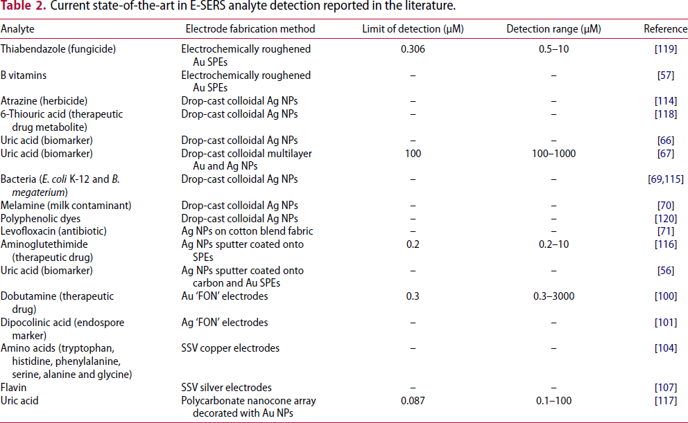
Current state-of-the-art in E-SERS analyte detection reported in the literature.
Outlook and conclusion
The aim of this review was to determine the most effective method of fabricating a NSE for E-SERS. To do this, it was necessary to define the requirements of such an electrode. These were identified as gold or silver nanoscale features; a regular structure with uniform nanogaps between features; fast electron transfer kinetics; a large surface area and a repeatable, reliable fabrication process. On top of this, there were practical considerations such as the ease, cost and length of the manufacture procedure. Currently, the most commonly used approaches fell into four main categories: EC roughening, colloidal NP deposition, ED and template-based methods. The assessment of these methods can be summarised very simply as: electrodes with large, repeatable SERS enhancements can be made but the processes are expensive and time-consuming; easier, quicker methods can also be used to create effective substrates, but they are much less uniform and reliable. Consequently, to determine the most effective fabrication method, one must consider the application.
In the case of biomarker detection, the appropriate substrate depends on the molecule being detected and the concentrations present. If the biomarker is a very effective Raman scatterer or present in high concentrations, an electrode with a lower SERS enhancement could still be part of a successful sensor. Conversely, if a biomarker is difficult to detect and only present at very low concentrations, large SERS signals are needed which would mean choosing a template-based fabrication method. It would also be necessary to consider the cost of the sensor in relation to its use case.
Ultimately, the aim is to develop fabrication methods that combine the qualities of the four approaches to create electrodes which are reliable, sensitive and cost-effective. The key avenues for future research fall into two main categories. The first is to apply the most promising developments from SERS research to E-SERS electrode fabrication. The use of complex shaped nanostructures that have been engineered to maximise ‘hot spots’, such as nanostars, NFs and nanourchins, have exhibited impressive EFs in a range of SERS applications and employing these structures in E-SERS would likely offer improved detection limits [18,22,35–37].
Furthermore, in recent years, heterogeneous nanostructures which contain two or more different materials, such as core–shell and hybrid NPs, have received increased attention [121–124]. Depending on the materials used, they can offer a range of benefits. For example, coating a plasmonic metal in a dielectric material can improve the stability of the NPs [125,126] and coating an inexpensive carrier with a noble metal can reduce the cost of plasmonic NPs [127]. Additionally, certain hybrid particles, such as gold core–silver shell NPs and plasmonic metal–semiconductor NPs, can exhibit charge transfer between the two materials which can lead to boosted SERS enhancements [30,67,128–136].
The second key avenue for future research is to utilise novel nanofabrication techniques to produce carefully controlled nanostructures in quicker and more cost-effective ways than the current template-based techniques. Possible approaches to investigate include nanoscale glancing able deposition [137,138], dip-pen lithography [139] and innovative self-assembly methods [140–142]. Developing a reliable, sensitive and cost-effective E-SERS electrode fabrication method requires innovation and creative thinking but there are already many promising approaches and the potential benefits of early disease detection make it a worthwhile challenge.
Footnotes
Disclosure statement
No potential conflict of interest was reported by the author.