
Abstract
Controllers for scanning probe instruments can be programmed for automated lithography to generate desired surface arrangements of nanopatterns of organic thin films, such as n-alkanethiol self-assembled monolayers (SAMs). In this report, atomic force microscopy (AFM) methods of lithography known as nanoshaving and nano-grafting are used to write nanopatterns within organic thin films. Commercial instruments provide software to control the length, direction, speed, and applied force of the scanning motion of the tip. For nanoshaving, higher forces are applied to an AFM tip to selectively remove regions of the matrix monolayer, exposing bare areas of the gold substrate. Nanografting is accomplished by force-induced displacement of molecules of a matrix SAM, followed immediately by the surface self-assembly of n-alkanethiol molecules from solution. Advancements in AFM automation enable rapid protocols for nanolithography, which can be accomplished within the tight time restraints of undergraduate laboratories. Example experiments with scanning probe lithography will be described in this report that were accomplished by undergraduate students during laboratory course activities and research internships in the chemistry department of Louisiana State University. Students were introduced to principles of surface analysis and gained “hands-on” experience with nanoscale chemistry.
Keywords
Introduction
Since the invention of atomic force microscopy (AFM) in 1986, 1,2 scanning probe methods for imaging and nanolithography have become increasingly valuable as tools for basic and applied research. Advances in computer software and hardware, and continued improvements of instrument designs have progressively improved the ease of use for scanning probe microscopes (SPM). Scanning probe instruments can be operated in a range of environments (ultra high vacuum [UHV], air, liquids) and can measure current, magnetic forces, surface charge, friction, electrostatic forces, etc. with nanoscale sensitivity. The imaging and measurement capabilities of scanning probe microscopes have been introduced for undergraduate laboratories in several disciplines including chemistry laboratories. However, the capabilities of SPM for nanolithography have not been as widely applied for undergraduate teaching. New trends in software and improvements in the automation of SPM instruments hold promise for bringing nanoscale experiments into the undergraduate curriculum, and eventually may even be integrated into high-school science labs. Optical microscopes have become common in educational labs for a wide range of science disciplines, and the next generation of young scientists will benefit from gaining skills with SPM instruments. To advance beyond the resolution limits of optical microscopes, SPM enables direct views, measurements, and manipulation of nanoscale phenomena.
A diverse range of experiments can be planned for educational lab exercises using SPM instruments, which have dozens of different measurement modes and instrument configurations integrated within a single instrument platform. The instruments are inherently a multidisciplinary toolkit because nanoscience measurements extend across all of the science disciplines of physics, chemistry, materials science, biology, medicine, and engineering. 3 For example, college laboratory exercises have been developed to illustrate principles of nanoscale measurements for magnetic, electronic, adhesive, or frictional forces. 4,5 A basic example would be to illustrate force—displacement profiles and calculations to demonstrate molecular bond rupture events by developing experiments using AFM probes with molecular coatings. 6,7 Other lab exercises could illustrate the imaging capabilities of AFM or scanning tunneling microscopy (STM), 8 particularly for resolving atomic or molecular lattices. 9 –14 Educational lab exercises with SPM have been reported for imaging surface changes caused by chemical reactions, 15 –18 nanopatterning, 5,19 and studies with biomolecules. 11,20 Student experiments with SPM provide 2D and 3D surface maps for illustrating the analysis of data such as height histograms, roughness measurements, and digital image processing. 21 Students obtain hands-on experience with molecules and nanoscience, and there are also intangible benefits of the ”wow“ factor for stimulating intellectual curiosity and enthusiasm for scientific discovery. Examples of SPM systems designed for college laboratories include instruments from NanoInk such as the NanoProfessor, 22 and the model 5400 system from Agilent. 23,24 These systems were designed with intuitive software and ease of use for installing probes and samples. Most of the laboratory time is occupied with the use of software interfaces, which minimizes possible damage to the scanners. Meanwhile, SPM probes are relatively inexpensive to replace, as a consumable item. Students can learn to tune in “slow TV” as the images are gradually generated on the computer monitor to reveal exquisite details of molecularly resolved surface landscapes.
Along with the unprecedented advantages for imaging and measurements of surfaces, a further compelling attribute of SPM instruments for educational activities are the capabilities for nanoscale manipulation of molecules and nanomaterials using scanning probe lithography (SPL), as described in this report. Significant advances in instrument automation to provide intuitive, user-friendly software offers exciting new possibilities for integrating cutting-edge technologies into the undergraduate laboratory curriculum.
Basic Operating Principle of AFM
The most common setup for positional feedback with AFM is the deflection-type configuration illustrated in Figure 1. An AFM tip is attached directly to a piezoceramic scanner for directing tip movement in the x, y, or z direction. The piezoceramic material of the scanner tube expands and contracts upon the application of small voltages causing movement at the level of angstroms. An electronic feedback circuit is used to control the amount of force applied between the tip and sample by adjusting the voltages sent to the scanner tube, to maintain a constant deflection of the cantilever. 25 The light of a diode laser is reflected off the back of the cantilever and detected by a position sensitive quadrant photodetector, as shown with the red lines of Figure 1. The amount of light impinging on the four photodetector elements changes as the tip is scanned across the surface, and the signals are used for positional feedback. As the AFM tip is scanned in a raster pattern, the up-down and left-right motion of the tip is profiled by the photodetector changes, and this signal is amplified and converted into digital images of topography and lateral force. Topographic images are maps of the surface morphology and are represented by an arbitrary color scale. Lateral force images indicate variations in the chemical nature of the molecules on the surface, which result from changes in the attractive and repulsive forces experienced by the tip. Topographic and lateral force images are acquired simultaneously. Most importantly, the force applied to an AFM tip can be precisely controlled at the level of nano- to pico-Newtons. 26 Low forces are used when characterizing surfaces to prevent unintentional damage to the sample, whereas higher forces are used for steps of nanofabrication for nanoshaving and nanografting of organic thin films.
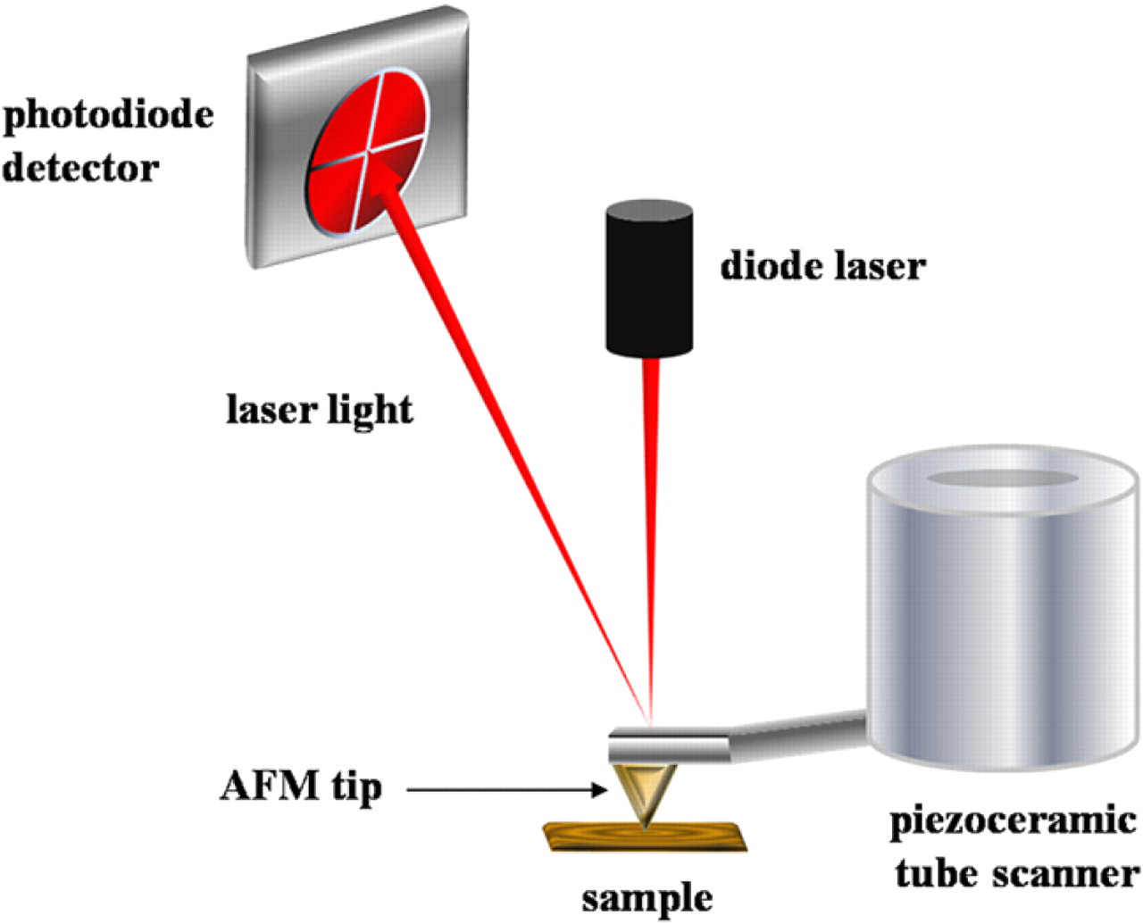
Basic instrument configuration for atomic force microscopy (AFM) imaging and nanolithography.
A typical setup for “contact-mode” AFM is presented in Figure 1, in which the tip is scanned in continuous contact with the surface. Other protocols can be accomplished by lifting the tip from the surface at a controlled distance for modes of ”non-contact“ imaging. A further imaging mode known as ”intermittent-contact“ mode is accomplished with a vibrating tip, which intermittently taps the surface, also known as ”tapping“ mode. Readers are directed to previous publications for further details of SPM imaging modes. 27,28 Images presented in this article were acquired using continuous contact mode AFM imaging.
Approaches for AFM-Based Nanolithography
Mechanisms for SPM-Based Nanolithography
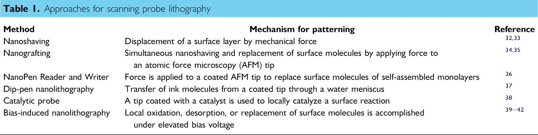
As methods for imaging and measurements with SPM were developed, researchers observed that under certain experimental conditions small areas of the surface could be accidentally altered or damaged. For example, when too much force was applied to the probe, the surface could be scratched or rearranged. Contaminants on the surface could be picked up by the tip and redeposited in other locations. Nanoscale lithography methods came to be developed by carefully controlling the changes that were made to surfaces, to selectively and intentionally change the chemistry of small areas under the tip. Bias-induced nanolithography, dip-pen nanolithography (DPN), catalytic-probe lithography, nanoshaving, nanografting, and NanoPen Reader and Writer (NPRW) are examples of SPL, which have different mechanisms for writing nanopatterns. 29 –31 The nature of the desired changes in surface chemistry will help determine which nanolithography methods are most suitable and convenient for experiments.
A summary of different techniques for writing nanopatterns using SPM-based lithography is presented in Table 1. Very little modification of AFM instruments is needed to accomplish nanolithography. Methods of nanoshaving, 32,33 nanografting, 34,35 and NPRW 36 require controlling the force applied to an AFM probe to inscribe patterns within self-assembled monolayers (SAMs). For DPN, the tip is coated with molecules or nanomaterials to be written. The writing of molecules on surfaces is accomplished by transfer from the tip through a liquid meniscus to a clean substrate. 37 For catalytic-probe lithography, an AFM tip is coated with catalyst molecules or metals. The coating is not transferred to the surface, instead the catalyst coating of the probe is used to catalyze a chemical reaction and selectively alter the chemistry of areas where the tip is placed in contact with the surface. 38 The catalytic reaction only occurs at areas touched by the tip. Bias-induced lithography is achieved using a conductive tip with a conductive or semiconductive substrate, in which an electric field is generated between the tip and the sample. As the AFM tip is scanned in contact with the surface at elevated bias, molecules are either oxidized, 39 desorbed, or replaced to create nanopatterns. 40 –42 Details of strategies and mechanisms for patterning with SPL have previously been reviewed. 30 –32,43 –48
Approaches for scanning probe lithography
Experimental Approach
Materials and Chemicals
Reagent grade dodecanethiol, octadecanethiol, 11-mercaptoundecanol (MUD), and 16-mercaptohexadecanoic acid (MHA) were obtained from Sigma Aldrich (St. Louis, MO) and used without further purification. Ethanol (200 proof) was purchased from AAper Alcohol and Chemical Co. (Shelbyville, KY). Flame-annealed ultra flat films of Au(111) prepared on mica substrates were obtained from Agilent Technologies, Inc. (Tempe, AZ).
Preparation of SAMs
Because of the ease of preparation, stability, and reproducibility for preparing well-ordered surface structures, SAMs of n-alkanethiols are good models for nanolithography experiments. Monolayer films of defined thickness and designed properties can be generated by changing the functional (head) groups of the alkyl chain; these functional groups can also be used for further chemical reactions in later chemical steps. The preparation, characterization, and properties of SAMs have been described and reviewed previously. 49 –52 Samples of matrix monolayer films were prepared by immersing gold substrates in 0.01 mM ethanolic solutions of the chosen n-alkanethiols for at least 12 h. The samples were then removed from the thiol solution, rinsed copiously with fresh ethanol, and placed into a liquid cell holder for AFM imaging and lithography. Ethanol solutions of MHA (10−6 and 10−9 M) and MUD (10−6 M) were freshly prepared for nanografting protocols.
Scanning Probe Microscopy
Experiments were accomplished in solution using either an Agilent 5500 SPM system or an RHK system interfaced with a PicoSPM scan head. The Agilent system was equipped with PicoScan version 5.3.3 software and PicoLITH beta v.0.6.0 for nanolithography. Images were acquired at a scan rate of 3.0 nm/s using 512 lines/frame. The RHK system was operated with XPMPro v1.1.0.9 software using SPM100 controllers. Oxide sharpened V-shaped silicon nitride probes from Veeco Probes (MSCT-AUHW, Santa Barbara, CA) were used for imaging and nanofabrication. The probes have an average force constant of 0.5 N/m. Image processing was accomplished using either Gwyddion software, version 2.5, which is freely available for download and is supported by Czech Metrology Institute 53 (Figs. 4, 5, and 7) or with PicoScan version 5.3.3 from Agilent (Fig. 8).
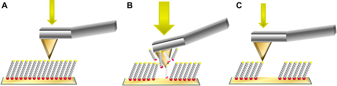
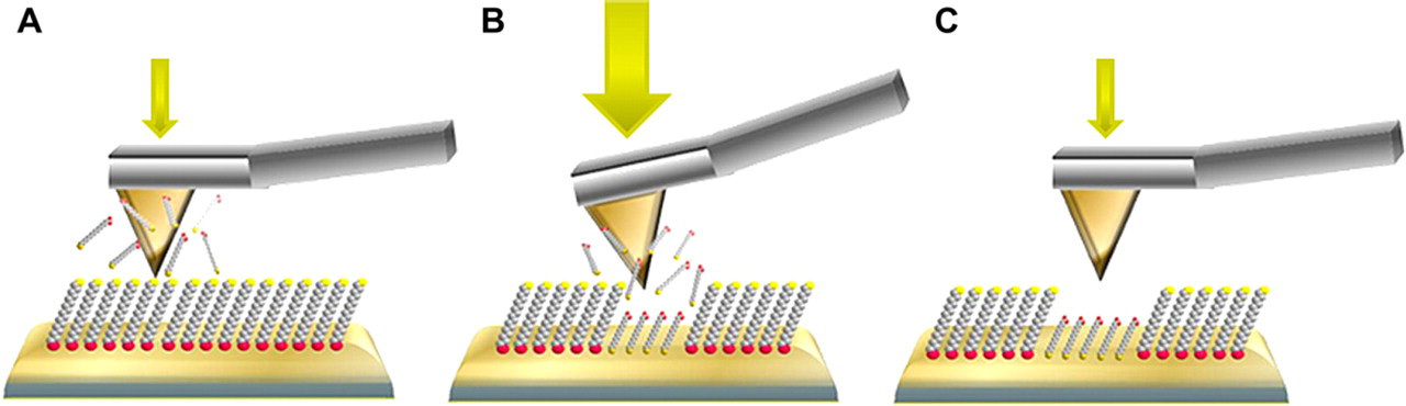
Basic steps for nanoshaving with an atomic force microscopy (AFM) tip operated under different forces. A. Characterization under low force. B. Nanoshaving is accomplished when the force is increased. C. Returning to low force, the nanoshaved patterns can be imaged.
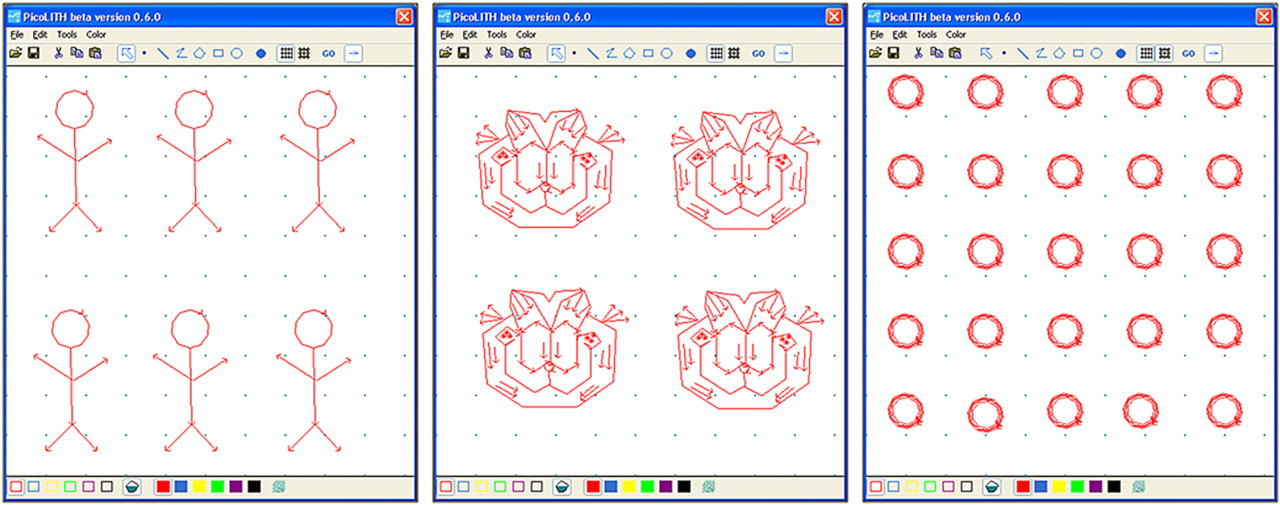
Example designs created using PicoLITH software by undergraduate students, during a physical chemistry laboratory at Louisiana State University. From left to right, sketches for patterns of stick people, cartoons of the face of a cat, and a 5 × 5 array of rings.
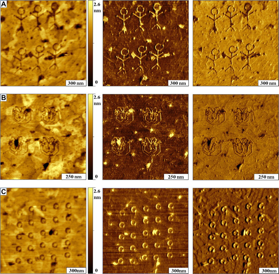
Nanoshaved patterns created with the designs of Figure 3 within a matrix monolayer of octadecanethiol on a gold substrate. A. Atomic force microscopy (AFM) topography view of six stick figures and the corresponding trace and retrace lateral force images (from left to right). B. Topography and lateral force images of the cat cartoon patterns produced with nanoshaving. C. Topography and lateral force images of an array of ring nanopatterns.
Example of nanopatterns produced by nanoshaving-selected regions of octadecanethiol using a scanning probe microscope (SPM) instrument from RHK Technologies. A. Contact mode topograph. B. Sketch for the corresponding patterns in (A).
Steps for nanografting are accomplished by scanning with a tip under high force, while the tip is immersed in a solution containing molecules to be written. A. Surface characterization is accomplished under low force while imaging in a solution containing thiol molecules. B. Nanografting is accomplished by increasing the force applied to the atomic force microscopy (AFM) tip; fresh molecules from solution assemble following the path of the scanning probe. C. Returning to low force, the nanografted patterns can be imaged.
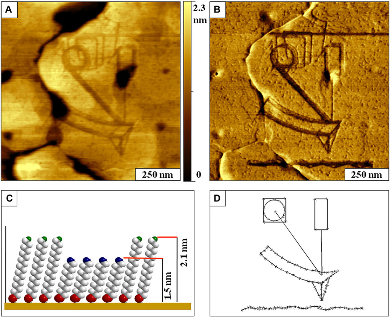
A nanoscale atomic force microscopy (AFM) instrument diagram written with 11-mercaptoundecanol within an octadecanethiol self-assembled monolayer (SAM). A. Contact mode AFM topograph for a 1 × 1 μm2 scan area; (B) corresponding lateral force image; (C) molecular model showing height differences between the pattern and matrix monolayer; (D) design used for nanografting.
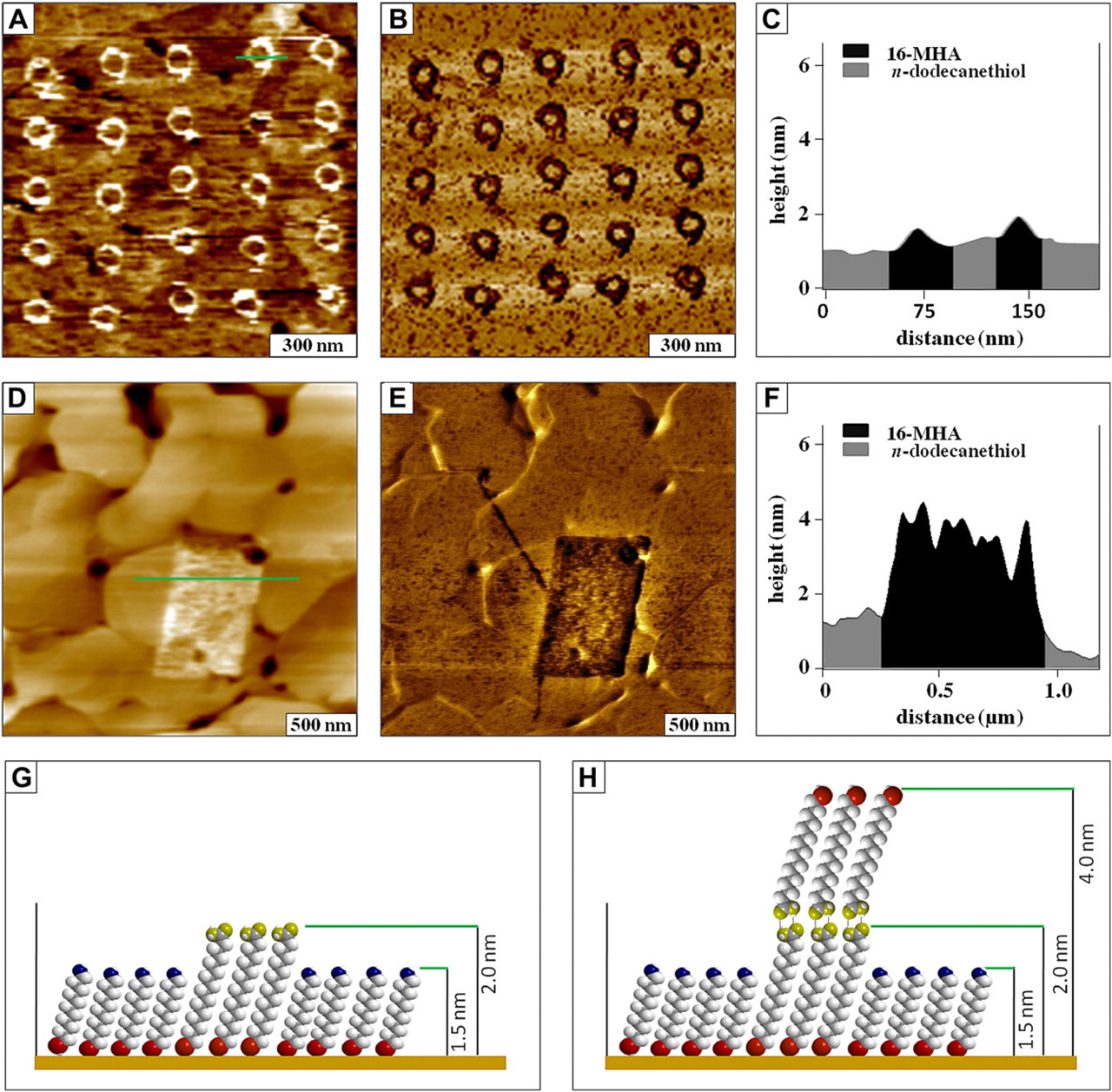
Nanografted patterns of 16-mercaptohexadecanoic acid written within a self-assembled monolayer (SAM) of dodecanethiol. A. Topography image (1.2 × 1.2 μm2) of an array of ring patterns; (B) corresponding lateral force image; (C) height profile for the line in (A); (D) topograph of a rectangular pattern (2.5 × 2.5 μm2); (E) lateral force image for (D); (F) line profile across the pattern in D; (G) height model for the nanografted pattern of A; (H) model of the double-layer pattern of (D).
Results and Discussion
Creating Patterns within a SAM Matrix Using Nanoshaving
Nanoshaving describes AFM-based methods of nanofabrication in which the tip is operated under force to uncover or scratch away selected regions of substrates that are covered with a matrix layer of an organic thin film. Nanoshaving can be accomplished in air or in liquid media. In air, the molecules that are displaced tend to accumulate at the edges of nanopatterns, whereas in liquid the displaced molecules can be dissolved in the surrounding solvent. Imaging in liquids has the advantage of improving resolution, because strong shear forces and tip-surface attraction caused by capillary forces in air are greatly decreased when imaging in liquids. 54,55 Nanoshaving is accomplished by applying a high mechanical force to an AFM tip as it is raster scanned across the surface to sweep away molecules of the surface layer as shown in Figure 2.
The process of nanoshaving is completed in three basic steps. First, a flat area of the surface is identified and imaged under low force (Fig. 2A). For the characterization step, typically forces less than 1 nN are applied to the probe to enable high-resolution characterization of the topography without damaging the sample surface. An area with few defects is chosen for inscribing patterns, preferentially a flat gold plateau that is wide enough to write the desired pattern sizes. Next, a greater force ranging from 1 to 10 nN is applied to the AFM tip to shave away the matrix molecules from the substrate as it is scanned with a pattern design (Fig. 2B). A sufficient amount of force is needed to ensure complete removal of the matrix SAMs without damaging the underlying gold substrate. After molecules are shaved away, the same AFM probe is used for imaging the newly fabricated patterns by returning to a low force (Fig. 2C). With careful control of the forces applied to the tip, hundreds of patterns can be fabricated within a few hours of an experiment. The uncovered regions created from nanoshaving are then available for deposition of new molecules and materials. 56 –58 Nanoshaving has also been used to provide information about the thickness of molecular layers on surfaces. 59,60 The uncovered areas of the substrate provide a baseline for thickness measurements of SAMs with angstrom precision.
Automated Nanolithography Using Designs Created with PicoLITH Software
Computer automation of scanning probe instruments enables the rapid fabrication of complex patterns with intricate designs and arrangements at the nanoscale to be a relatively routine accomplishment. Patterns with nanometer dimensions can be readily achieved with precision and accuracy using software that controls the position, force, bias, and speed of the probe. Example designs used for creating nanopatterns are shown in Figure 3 using PicoLITH software from Agilent. Automated nanoshaving is more complicated than producing images for a computer printer, because the user must consider where the tip is picked up or placed down on the surface. When the tip is picked up and placed down, this can lead to gaps or stray marks for designs. Better fidelity is achieved when the tip is moved continuously across the surface without removing the tip. The analyst will need to experiment with different designs to determine how many times to outline the features to observe which scanning paths work best for sweeping material from the surface. Sketches of the desired patterns are outlined with PicoLITH scripts using a computer mouse or pen stylus to draw the patterns. For the examples in Figure 3, arrows indicate the writing direction for translating the AFM tip. The overall size of the patterns is defined by the size of the view window selected within the data acquisition window of the PicoSPM operating software, for example, 1 × 1 μm2. Patterns can be outlined once or traced several times. The colored squares at the bottom of the PicoLITH design (Fig. 3) are the scientific pallets that can be used to assign specific parameters for operating the probe. For example, experimental parameters for the speed, amount of force, or bias voltage applied to an AFM tip are assigned by choosing a color and assigning values. Automated lithography with an RHK SPM is accomplished with a computer controlled vector scan module as previously described by Cruchon-Dupeyrat et al. 61 Computer statements to control the motion of the probe are written and compiled into lithography scripts to designate the writing speed, length, direction, and force applied for inscribing nanopatterns.
Writing Patterns of SAMs with Nanoshaving
Patterns for the designs of Figure 3 with different shapes and geometries written are shown in Figure 4, for nanoshaving within a matrix SAM of n-octadecanethiol. Octadecanethiol has 18 carbons aligned in a chain as the backbone of the molecule, and is anchored to the surface by a gold-sulfur bond. The headgroups at the surface of the molecular layer are methyl groups (CH3), and the overall thickness of the SAM film is approximately 2.1 nm. Topography images acquired with AFM are displayed by a selected color scale; in this report, the shorter features are dark and taller structures are brighter in color. Nanoshaving was accomplished in ethanol by applying a high force to the AFM tip as it was scanned, to sweep away and remove selected areas of the matrix monolayer from the gold surface following the outline of the designs shown in Figure 3. After writing patterns, the same AFM probe was used to immediately characterize the patterns in situ. The images in Figure 4 reveal intricate details of the surface morphology of octadecanethiol as directly viewed by nanosize defects such as scratches, scars, pinholes, and etch pits. Overlapping terrace steps and the outlines of the gold substrates underlying the SAM are also visible in the images. Although the surface may appear somewhat rough, the terrace steps are only 0.25 nm in height and are characteristic landmarks of a high-resolution image of a SAM. At the nanoscale, even very small features such as etch pits, which are only 0.2 nm deep can be resolved using AFM. The small holes scattered over the surface are commonly called etch pits (also known as molecular vacancy islands), which are produced by surface reconstruction. 62 The fine details of the irregular contours of the edges of the gold terraces can only be observed with a sharp tip. Such highresolution images can be routinely acquired by using AFM in liquid environments.
Figure 4A displays images of six stick people inscribed within octadecanethiol using nanoshaving. The images and nanopatterns were produced by undergraduate students during a 3h laboratory session of Physical Chemistry (Chem 3493). The trace and retrace lateral force images do not show height information, rather the changes in tip-surface friction are mapped to disclose variations in surface chemistry for the areas of the nanopatterns. Lateral force images are acquired simultaneously with contact mode topography images and provide additional chemical information of the sample nature. For these examples, the tip-surface adhesion between the AFM tip is markedly different for the uncovered gold substrate of the nanopatterns compared side by side with the methyl-terminated molecules of the SAM matrix areas. The patterns of stick people were written using a single pass of the AFM probe to outline the design and were completed in 1 min. The line width measures approximately 10 nm, and varies according to the sharpness of the AFM probe.
A more sophisticated pattern was nanoshaved (Fig. 4B) to outline a cartoon of a cat design. This example was accomplished within 3 min using a writing speed of 0.1 μm/s and an applied force of 2 nN. The speeds used for nanoshaving are comparable to the optimized speeds for acquiring images; of course, if the tip is rastered too quickly it can break contact with the surface to produce discontinuous patterns. One might be concerned that operating an AFM tip under force might cause it to become dull or break the apex of the probe; however, this example exhibits superb resolution for resolving etch pits, pin hole defects, and the lacey contours of step edges, despite having used the tip under force for nanoshaving. We have found that silicon nitride probes are quite robust within the typical operating range of 2–10 nN of force used for SPL. Often the tip becomes sharper and resolution improves over time when nanoshaving. The patterns of Figure 4B were traced once and measure 7 nm in line width. Using nanoshaving, 25 ring patterns were inscribed within an octadecanethiol SAM (Fig. 4C); however, for this example the designs were outlined four times. A force of 2 nN was applied for nanoshaving to produce rings measuring 80 nm in diameter with widths of 18 nm. Scanner hysteresis and drift can produce small changes in the nanoscale registry of the pattern arrangements, as viewed for the misalignment along the × direction. This is likely caused by using too much force to write the patterns, leading to a slight drift in probe motion across the array of ring designs. However, the precision for writing rows of patterns in the y direction is near perfect, with uniform 100-nm spacing between each ring in the x and y directions.
Automated SPL Using Computer Scripts
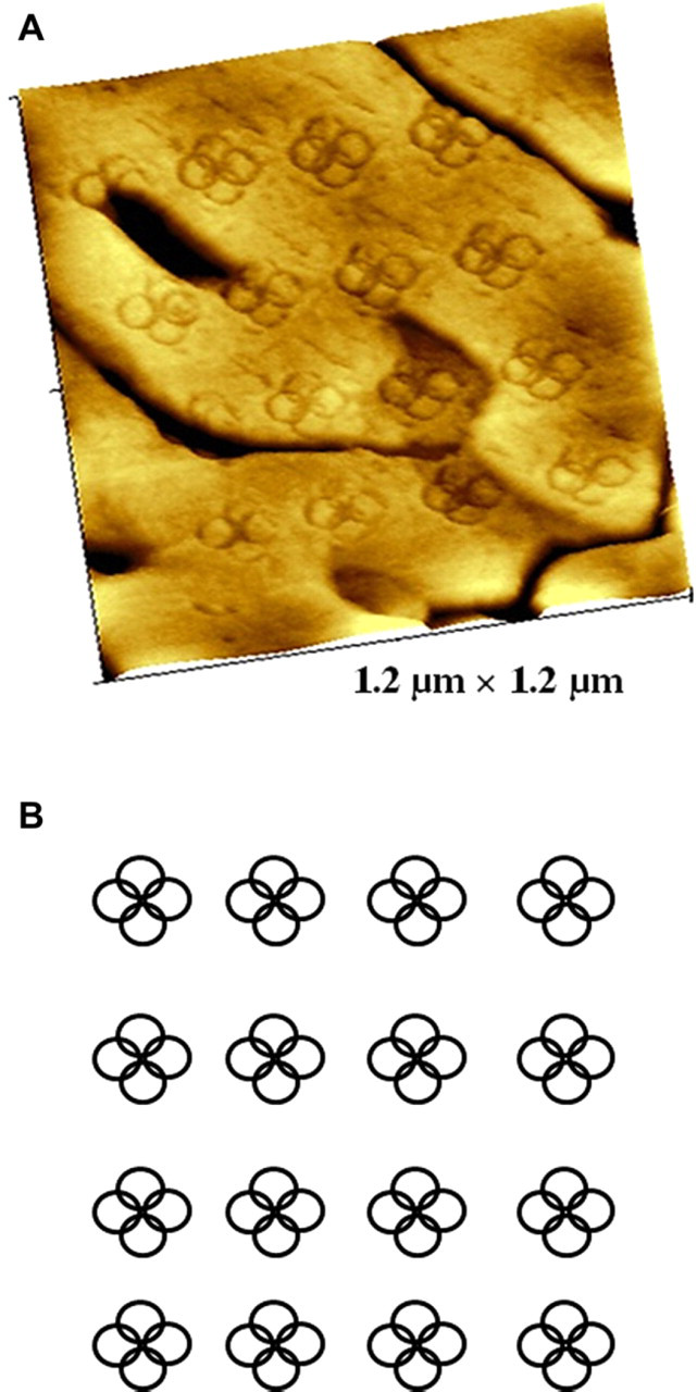
Examples of 16 nanoshaved patterns of interconnected circles created within octadecanethiol are presented in Figure 5, generated with an in-house-designed computer script with an RHK controller. The exquisite reproducibility for controlling nanoscale lithography is evidenced by the precise, regular shapes and interpattern spacing and alignment at the nanoscale. The topography frame of Figure 5A shows a 1.2 × 1.2 μm2 view of the nanopatterns and the corresponding design is sketched in Figure 5B. The design of each pattern was produced by outlining four circles with a common focal point. The rings are shallower than the surrounding monolayer of octadecanethiol. Each individual ring measures 60 nm in diameter, with the smallest line width measuring approximately 10 nm. A few stray marks are apparent above the patterns, which results from up-down translation of the tip when it is picked up or placed at locations for writing. For this example, the scars of the underlying gold film influence the brightness of the image color scale, because the nanoshaved patterns are shallower in depth (2.1 nm) than the defects of the substrate (10 nm). However, the fidelity of nanoshaving for writing precise nanoscale designs can still be sufficiently well resolved at this size scale.
Using Nanografting to Write Designed Patterns of n-Alkanethiols
Nanografting is likewise accomplished by increasing the force applied to an AFM probe; however, instead of operating the tip in clean solvent, the imaging media was replaced with a freshly prepared, dilute solution of n-alkanethiols to be patterned. Nanografting was developed in 1999 by Xu et al. 35 and since then it has been used for writing a range of molecules with thiol groups. 30 Similar to nanoshaving, there are three basic steps for nanografting as outlined in Figure 6. In the first characterization step, a flat area that has few defects is selected for inscribing patterns by imaging under low force, typically less than 1 nN (Fig. 6A). Next, the force is increased to push through the surface monolayer to make contact with the gold surface underneath. As the tip is scanned under force, the matrix molecules underneath the tip are shaved away and immediately replaced with new molecules from the surrounding solution (Fig. 6B). Following the scanning path of the AFM tip, molecules assemble and bind to the areas of gold that were uncovered by the probe to produce designed patterns. Returning to low force (Fig. 6C) the same probe is used to characterize the nanopatterns that were fabricated. When the tip is operated under low force, the surface is not disturbed and no patterns are formed. Patterns are produced only when the force has been increased.
When designing nanografting protocols, the analyst can choose from a range of commercially available thiol molecules with different lengths and head group chemistries. Examples are shown in Figure 7 of nanografted patterns with heights that are shorter than the matrix monolayer. The topography and corresponding lateral force images of the design for an AFM instrument schematic are presented in Figure 7A, B, respectively. The instrument components were described previously in Figure 1. Characteristics of the general morphology of an n-alkanethiol SAM are apparent in the topography frame, such as etch pits and terrace steps. The lateral force image more prominently reveals the pattern design, because the headgroups of the pattern areas are chemically different than the matrix SAM, which provides frictional contrast. The areas surrounding the pattern are methyl-terminated octadecanethiol and the patterns were written with hydroxyl-terminated MUD, which is 0.6 nm shorter than the matrix SAM. A model of the molecular heights is shown in Figure 7C. The script used to outline the nanopatterns is shown in Figure 7D, with excellent correspondence between the design and resulting nanografted patterns for such small size scales. The smallest line width achieved for this pattern was accomplished with a single sweep for the vertical line between the backside of the cantilever and the diode laser, measuring 13 nm in width. With an ultra sharp AFM probe, the smallest feature produced with nanografting is an island of a 2 × 4 nm2 dot pattern, which is an area that would accommodate approximately 32 thiol molecules. 63
Examples of nanografted patterns with heights that are taller than the matrix monolayer are shown in Figure 8. Interestingly, the same molecules were used for Figure 8A, D; however the concentration of the imaging media was increased for Figure 8D. The topography and corresponding lateral force images of an array of ring patterns shown for the design of Figure 3 are presented in Figure 8A, B, respectively. At low concentration (10−9 M), MHA forms patterns with heights corresponding to a monolayer. For these examples, the matrix monolayer is dodecanethiol, which has 12 carbons in the hydrocarbon backbone chain. Dodecanethiol is ∼0.5 nm shorter than MHA, which is consistent with the height measured for a line profile across one of the nanopatterns (Fig. 8C). When the concentration of the imaging media of MHA was increased to 10−6 M, molecules with carboxylic acid-terminated headgroups form dimers and assemble to generate double layers (Fig. 8D). 64,65 Dimers of MHA are produced in solution by coupling of the acid head-groups. Height models of the MHA nanopatterns are shown in Figure 8G and H for the single- and double-layer patterns, respectively. The acid headgroups of the nanopatterns exhibit strong tip-surface adhesion, producing line spike artifacts in the topography frames. The differences in surface chemistry between the nanografted patterns (carboxylic acid headgroups) and the dodecanethiol matrix SAM (methyl headgroups) provide excellent contrast for the lateral force image of Figure 8B. However, for the lateral force image of Figure 8E, the headgroups of the rectangular pattern are most likely terminated with a thiol endgroup.
These examples of nanografted patterns illustrate the inherent capabilities of SPL for three-dimensional (3D) control of nanostructures by selecting the molecular length, head-groups, and pattern geometries. Nanoscale characterizations and lithography are valuable tools for directly studying surface chemical reactions at the nanoscale within a well-controlled, liquid environment. After producing nanopatterns with nanoshaving or nanografting, further chemical reaction steps can be accomplished by exchanging the imaging media, for example by introducing solutions of new molecules, 58 copper salts, 66 or proteins 67,68 to build complicated architectures from the bottom-up.
Applications of Scanning Probe Nanolithography
SPL approaches such as nanoshaving and nanografting with organic thin films extend beyond simple fabrication of nanopatterns to enable control of surface composition and reactivity at the nanoscale. Methods to precisely arrange molecules on surfaces already contribute to discoveries that are advancing future technologies in molecular electronics, nanomedicine, and surface chemistry. Automation of SPL will likely have a significant role for implementing nanotechnology in commercial products.
Impact of SPL for Advancements in Molecular Electronics
Writing individual patterns of organic films one at a time will not be a practical strategy for manufacturing devices in which billions of structures are needed, such as for designs of computer memory chips and circuits. Future nanotechnology applications will require much higher throughput and speed for generating patterns. This problem is being addressed by the development of arrays of multiple probes for parallel writing. 69,70 For semiconductor-based technologies, organosilane thin films are widely used as resist layers for microfabrication of circuits, wires, transistors, and memory chips. As the size of components achieves ever-smaller dimensions, the inherent advantages for miniaturizing to the nanometer level will be the benefits of higher information density and faster processing time. Nanotechnology holds promise for advantages of smaller, cheaper, and more energy efficient electronic devices. To achieve smaller elements will require molecular-level precision such as the capabilities provided by automated SPL.
Application of SPL for Nanomedicine
Nanoscale assays provide intriguing possibilities for the direct detection and in situ visualization of the binding of small molecules, DNA, antibodies, or proteins to nanopatterns, while enabling surface changes to be monitored with time-lapse AFM images. 29,30 Nanostructures of SAMs written by SPL provide highly controllable test environments for exquisite images of surface changes during biochemical reactions. 71 Although electron microscopies can be used for high-resolution 2D imaging of biomolecules that have been freeze dried and sputter coated with conductive films, reactions conducted in aqueous (physiological) media or buffers cannot be accomplished in the UHV environments of electron microscope chambers. Approaches with SPM provide 3D images of fragile biomolecule systems and cells with minimal sample preparation. Tools of SPL extend the capabilities of high-resolution scanning probe imaging to enable experimentalists to control surface arrangements of biomolecules at the molecular level. Examples of fundamental studies incorporating tools of SPL for investigations of biomolecules include the regulation and control of multiplexing, reactivity, and polyvalent interactions; nanoscale assays with oligonucleotides 72 or receptors for sensing or bioassays 73,74 ; and construction of DNA 75 –78 and protein 67,68 nanostructures.
Role of SPL for Fundamental Investigations of Surface Chemistry
Intuitively, binding between molecules is a nanometersized phenomenon; thus, a close-up view of molecules on surfaces can provide a fresh perspective for mechanisms of how reactions occur. Nanografted patterns can be incubated with desired nanomaterials or molecules, and time-lapse AFM provides direct views to monitor the successive changes in height and surface morphology as reactions proceed over time. The reaction sites are spatially constrained to nanosized areas defined by the headgroups of nanografted/nanoshaved patterns, providing exquisite control of reaction parameters at the nanoscale. Such studies provide insight about surface reaction mechanisms and kinetics. For example, in situ investigations with nanografting have been reported for adsorption of proteins, 57,79 –81 electroless deposition of copper on nanografted SAMs, 66 templated growth of ionic self-assembled multilayers, 82 and pattern transfer reactions with polymers. 58
Underlying Themes for Undergraduate Instruction
The take-home message from a scanning probe lab exercise would perhaps be that we “looked at molecules” and learned how to write nanopatterns on surfaces. The existence of atoms or molecules in materials is a critical concept for understanding chemistry and physics, along with calculations of the size and number of molecules/atoms that are present. Many students have difficulties in understanding concepts of atomic and molecular scale phenomena, and the challenge of visualizing the shapes and arrangements of atoms and molecules has been implicated as a core issue. 14 Scanning probe experiments offer premiere opportunities for students to learn interactively to visualize surfaces, measure properties, and to manipulate surface chemistry at resolutions down to molecular and atomic length scales. Advancements in software and automation have made scanning probe instruments relatively easy to operate, and the new capabilities are ideally suited for undergraduate laboratories. As the field of nanoscience research has evolved, SPM methods have mostly been limited to professional researchers and graduate students; however, there is increasing interest for advancing nanoscience education at the undergraduate level. 83 Our practical strategy at Louisiana State University has been to accomplish undergraduate teaching activities using our research instruments, with the slight expense of a few broken probes.
The background information to be presented for SPM laboratories will depend on the timeframe and type of experiments that are designed. A complete grasp of nanoscale concepts most likely exceeds the scope of an undergraduate course. However, a basic introduction and illustration of selected topics of nanoscience can certainly be accomplished to provide a spark for future student interest. During the past 4 years at Louisiana State University, we have successfully integrated SPM modules into the third-year undergraduate physical chemistry lab course. During each semester, 12–16 students are given an opportunity for hands-on experiments with AFM/STM instruments. One session is devoted to an introduction of the basic principles of nanoscale imaging and instrument operation, and a second session is used for nanolithography experiments. As an indicator of the level of student enthusiasm, the afternoon class is scheduled for 3-h duration, but usually several students persist late into the evening to capture additional frames and to experiment with designs for writing nanopatterns (Fig. 9). From these classroom groups, 30 undergraduates have further elected to take additional hours of supervised research credit, choosing to work with projects using SPM. The undergraduates have all made contributions as coauthors of research posters and/or journal articles, and have participated in fundamental studies with systems of nanoparticles, proteins, or SAMs.
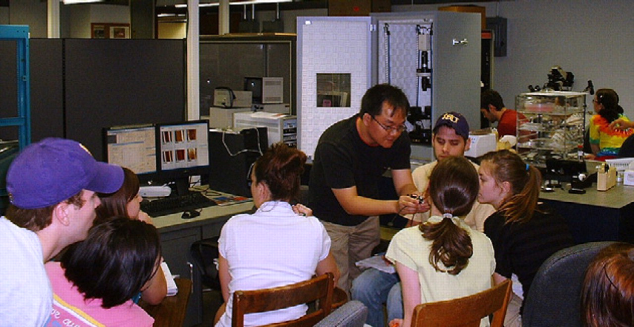
Undergraduate students from an Louisiana State University physical chemistry laboratory engaged in learning new skills with an atomic force microscopy (AFM) instrument.
Future Prospectus
Impressive accomplishments have been attained by manufacturers of scanning probe instruments for the automation of SPL and for providing user-friendly software for routinely imaging at the nanoscale, as evidenced by the nanofabrication examples of this report. One can easily predict that such capabilities will become ever more widely applied in education, research, and technology in the near future. There is an emerging need for workers with scanning probe skills, because methods of SPM and SPL are becoming indispensable for fundamental investigations related to nanotechnology. Data published on the National Nanotechnology Web site (http://www.nano.gov/) estimates that 20,000 researchers are currently working in nanotechnology worldwide, and the National Science Foundation has estimated that two million workers will be needed to support nanotechnology industries globally within 15 years. 84
A skilled scientific workforce will be an essential requirement for implementing nanoscience discoveries in future manufacturing or technology applications. Knowledge and experience in modern methods of surface measurements and analysis will be pivotal to the rapid transfer of nanotechnology into commercial products. At present, scanning probe microscopes and scanning probe-based lithography are primarily used for laboratory research investigations rather than as tools for manufacturing. The transfer of new technologies developed in academic research labs to the public sector will require dissemination of skills and information from cutting-edge nanoscience research to the undergraduate curriculum across scientific disciplines. The latest advances in automation of SPM instruments enable new possibilities for educational modules using SPL, providing opportunities for designing diverse and compelling student activities to teach the concepts of chemistry and nanoscience, showcased at the molecular level.
ACKNOWLEDGMENT
The authors gratefully acknowledge financial support from the National Science Foundation (DMR-0906873), NSF (2005–10) LAMP-PHASE III-9, and the National Institutes of Health (R25GM069743–06). T.T.B. appreciatively acknowledges the Office of Strategic Initiatives (Howard Hughes Medical Institute Professor's Program and Integration of Education and Mentoring Program), the Louis Stokes Louisiana Alliance for Minority Participation, and the Louisiana State University Initiative for Maximizing Student Diversity program for scholarships to promote undergraduate research. They would also like to thank Dr. J. Ngunjiri, Dr. A. Kelley, K. Lusker, S. Daniels, and W. Serem for their dedication to undergraduate mentoring and participation in this research effort. Treva T. Brown received the Analytical Systems Digital Library Young Scientist Award from the Association for Laboratory Automation.
Competing Interests Statement: The authors certify that they have no relevant financial interests in this article, and that all financial and material support for this research and work are clearly identified in the article.