
Abstract
Nanopore sensors are expected to be one of the most promising next generation sequencing technologies, with label-free, amplification-free and high-throughput features, as well as rapid detections and low cost. Solid-state nanopores have been widely explored due to their diverse fabrication methods and CMOS compatibility. Here, we highlight the fabrication methods of solid-state nanopores, including the direct opening and the tuning methods. In addition, molecular translocation developments, DNA sequencing and protein detections are summarized. Finally, the latest progress relating to solid-state nanopores is discussed, which helps to offer a comprehensive understanding of the current situation for solid-state nanopore sensors.
1. Introduction
In recent years, advances in the “Nano-Bio” research field have prompted a great deal of interest in the scientific world. Nanoscale tools serve as ideal interfaces to interrogate biological systems, since the sizes of many nanostructures are comparable to those of typical biomolecules. Among them, nanopore sensors have been highlighted as potential tools to detect individual biomolecules [1–10]. By mimicking the functions of natural biological ion channels, nanopore sensors can control access and selectively identify for biomolecules at the single molecule level. The principle of nanopore sensing is based on the Coulter counter technique [11, 12]. As shown in Figure 1, an ultra-thin membrane with a nanoscale pore separates two reservoirs filled with electrolyte solutions. Ionic current information is created by electrically driving the individual biomolecule into a nanopore. Furthermore, by analysing the ionic current signature, a molecule's conformation, as well as structural and chemical properties of the biomolecules, can be obtained.
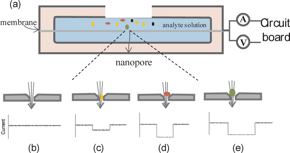
Nanopore principle scheme: (a) the profile of the device; (b-e) different analytes passing through the pore, which will create characteristic signals
Currently, there are three major types of nanopores: biological nanopores, solid-state nanopores and hybrid nanopores. The biological nanopores are mainly created from natural protein molecules (e.g., channel proteins), which present precisely controlled structures and interfacial chemistry [13, 14]. However, the biological nanopores are limited by a short life time, intrinsic instability and the strict requirement of a specific environment, which are not favoured for a device's long-term operations. Solid-state nanopores are usually fabricated by top-down lithography, which have the advantages of higher stability, precisely tunable size, robust chemical and thermal characteristics, and CMOS compatibility [15–17]. The detection principles of the nanopores are distinguishing the current fluctuations induced by analytes passing through the nanopores. If analytes are within identical spherical shapes, it is easy for solid state nanopores to distinguish different sizes of the analytes by the recording amplitude of the current fluctuations [18]. However, if the analytes show a little difference in shape and size, the detection results of solid state nanopores are usually unsatisfied [19]. This has been improved by introducing specific interactions between nanopores and analytes by assembling pore-forming synthetic soft materials inside solid-sate nanopores; these are referred to as hybrid nanopores. By combining specific surface chemistry, the drawbacks relating to the solid nanopores can be overcome and the detection limit of nanopore sensors can be improved [20, 21].
This review focuses on solid-state nanopores. We will first introduce the principle of nanopore sensors, and then present fabrications and applications of solid-state nanopores. Furthermore, recent advances, challenges and opportunities of nanopore sensors are discussed as well.
2. Principle
Due to the small size of the sensors, nanopore sensors are capable of detecting small objects (e.g., nanoparticles), even at the individual molecule level [22]. The principles of the detection process and the equivalent circuit are shown in Figure 1. An insulating membrane containing a nanometre pore is sandwiched between two reservoirs filled with electrolytes [14, 23, 24]. Ions are driven through the nanopore to generate an ionic current with the applied voltage. The conductivity of the apparatus remains stationary in a pure electrolyte solution and the current is a constant value with only a few fluctuations, which happens if there are no objects passing through. When analytes are added to one side of the chamber, they can be electrophoretically driven through the pore. A current blockage is created when an object passes through the nanopore. The measurable signal is determined mainly by two factors: steric exclusion and ion polymer properties. Steric exclusion can decrease the effective pore diameter and decrease the current. An ion polymer contains two parts: one is for co-ion repulsion, which will decrease the current, and the other is for counter-ion attraction, which will increase the current. Furthermore, these factors are all affected by the target concentrations. By increasing the concentration of the free analytes, the appearance frequency of the blockage current will increase. It provides a direct measurement of the frequency content, which contains the characteristic timescales of the analyte-nanopore interactions. Therefore, we can analyse the abundant bimolecular properties from the current information, such as their size, charge, length and specificity.
3. Fabrications of Solid-State Nanopores
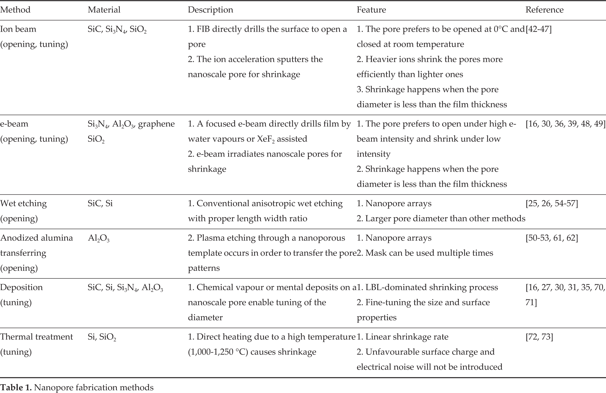
The solid-state nanopores have gained increasingly attention because of their high stability and potential to be produced on a large scale. A variety of materials have been successfully utilized in fabricating nanopores, such as silicon [25, 26], silicon nitride [27], silicon oxide [28–30], polymers [31, 32], aluminium oxide [33, 34] and graphene [35–41]. The general nanopore fabrication process can be divided into the opening and the tuning methods. The opening methods include focused ion beam (FIB) drilling [42–47], electron beam (e-beam) drilling [16, 30, 36, 39, 41, 48, 49], anodized alumina oxide transferring [50–53] and the wet etching method [25, 26, 54–57]. However, in most cases, the pore, with the desired size and shape, cannot be obtained directly. Extra tuning steps are normally required, such as deposition and thermal treatment. By combining all of these techniques, different sizes, shapes and properties of nanopores can be fabricated. Table 1 summarizes the features of these methods.
Nanopore fabrication methods
3.1 Direct opening methods
FIB involves a direct drilling method, which can create nanopores in specific areas relating to different types of membranes [47, 48, 58]. It was reported as the first technique for fabricating a single nanopore in 2001 by Li et al. [47]. The drilling process is shown in Figure 2(a). Li et al. used an Ar+ ion beam to drill a nanohole in a free-standing silicon nitride (Si3N4) membrane with a cavity on its opposite surface. A feedback detector was attached below the ion beam machine to indicate the stop point when the ions penetrated the membrane. By controlling the exposure time of the ion beam, the size of the nanopore can be well controlled. In addition, some critical parameters during the FIB process are also important in order to adjust the pore size, which will be discussed in 3.2.
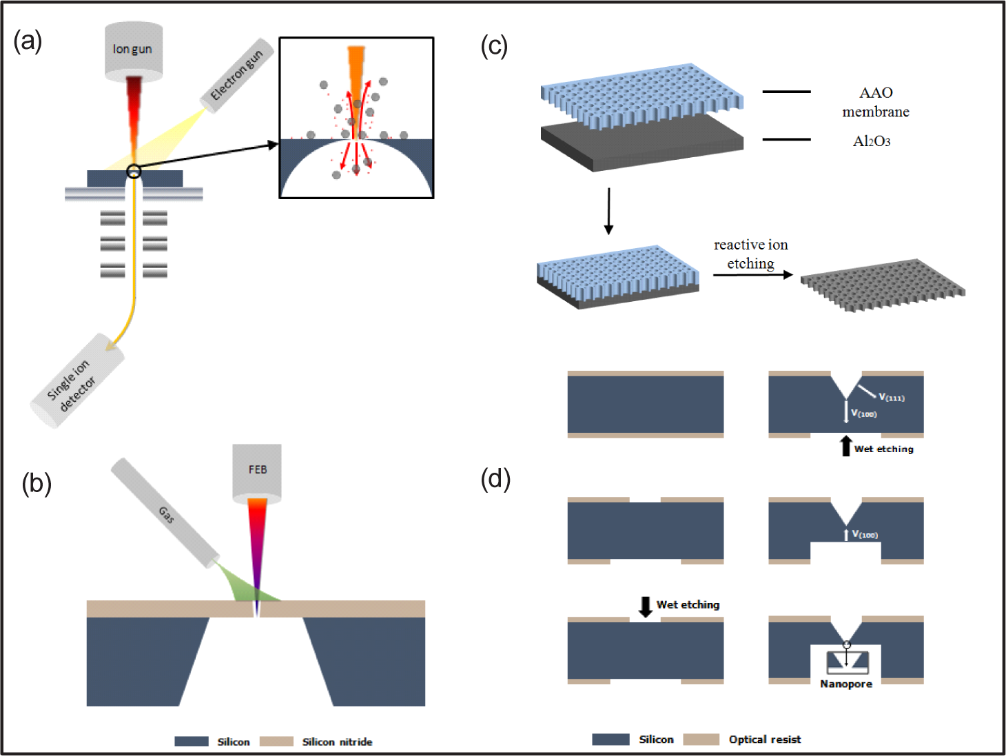
Schematic illustration of the nanopore fabrication process: (a) FIB, (b) e-beam, (c) anodized alumina transferring and (d) wet chemical etching methods
An intense e-beam is involved in another common method to fabricate nanopores [16, 30, 36, 39, 48, 49]. The first reported example using an e-beam to drill nanopores was Storm et al. [59]. An e-beam can fabricate nanopores in the range of 2–200 nm by manipulating the beam parameters, such as current, intensity and dwell time. However, the diameter of the nanopore is limited to the thickness of the membrane. In order to prepare nanopores with high precision in feature size, auxiliary gases are introduced. Yemini et al. first reported etching Si3N4 using XeF2, which eventually resulted in 17–200 nm nanopores in the Si3N4 membrane [49]. The drilling process is shown in Figure 2(b). Furthermore, Kim et al. found that the intensity of e-beam determines the formations of the nanopores: (a) nanopore expansion is caused by atom sputtering at higher intensities, while (b) surface-tension-driven nanopore contraction occurs at lower intensities [60].
Anodized alumina oxide transferring can be used to fabricate nanopores as well; see Figure 2(c). This method utilizes plasma etching through a nanoporous template to transfer the pore patterns onto the underneath substrates [50–53]. A typical nano-alumina template can be created by electrochemical anodization of aluminium film, which is rather easy compared with FIB or e-beam fabrications, while the templates can be used multiple times [61, 62]. Another advantage of this masked method is that the nanopore array can be efficiently fabricated.
Besides directly nanodrilling, wet chemical etching, which follows the standard micro-scale lithography process, has been demonstrated to be an alternative nanopore fabrication technique. The advantages of this method are simple and cost-effective, as well as offering multifunctional characters [25, 26, 54–57]. Figure 2(d) shows a typical wet etching process. First, a standard micrometre pattern is fabricated by the standard lithography process, then an inverted pyramid structure with a sharp tip on the bottom is created using anisotropic wet etching. Finally, nanopores are formed by etching the back on the other side of the substrate using alkaline solutions (e.g., KOH). Given the different etching rates in each of the crystal faces, anisotropic wet etching can fabricate nanopores with conical or pyramidal geometries, in contrast to the cylindrical inner structures drilled by FIB or e-beam. Nanopore arrays can be efficiently fabricated by wet etching as well [63, 64].
3.2 Tuning methods
In order to obtain the desired dimensions of the nanopores, a tuning process to further enlarge or shrink the nanopores is usually required following direct drilling. In FIB tuning, temperature plays an important role in pore opening and shrinking. According to the experiments of Li et al. [47], when an Ar ion beam is sputtered on the edge of the nanopore at room temperature, the pore prefers to be closed, since a very thin (∼5 nm) stressed viscous surface layer is created by the ion beam energy. However, when the temperature is reduced to 0 °C, the nanopore prefers to be opened [59, 65, 66]. Besides the temperature, the type of ions has an effect on the shrinkage of the pore. The shrinkage happens when the diameter of the pore is smaller than the thickness of the membrane [47, 48, 58]. Heavier ions (He, Ne, Ar, Kr and Xe) can shrink the pores more efficiently than lighter ones [67, 68]. By fine tuning these factors, nanopores with desired diameters can be fabricated.
The e-beam can tune the nanopores as well. When the membrane is exposed to a higher intensity of e-beam, the size of nanopore tends to be expanded through atom sputtering. On the other hand, a lower e-beam intensity will lead to nanopore shrinkage [60]. In addition, similar to the FIB, nanopore shrinkage also happens when the diameter of the pore is smaller than half of its thickness [49, 69].
Deposition of nanoscale thin films on nanopores is another effective method to decrease the pore diameter. Atomic layer deposition is one of the most popular deposition methods. Deposition of thin polymer films through a layer-by-layer (LBL) assembly approach has been reported to shrink nanopores; this approach also has great advantages in terms of low cost and the ability to tune the surface chemistry of the nanopores [16, 27, 30, 31, 35, 70, 71].
Direct annealing can shrink the nanopore as well [72, 73]. In contrast to FIB and e-beam shrinkage, thermal treatment can change the morphology of the nanopores. For a silicon dioxide (SiO2) membrane, it was found that, at the appropriate temperature (1,125 °C), the average shrinking rate of the pore is ∼22 nm per minute. Meanwhile, at a lower temperature (<1,000 °C), the diameter of the pore shows little or even no change. When the nanopore is exposed to a higher temperature (>1,250 °C), the SiO2 membrane may be broken, while the shrinkage rate is too fast to be controlled. Another advantage of thermal shrinkage is that it will not increase the noise of the electrical signal of the nanopore sensors, since no additional surface charge is added.
4. Applications
Due to the simple operating principle of nanopore sensing and the technology available for nanopore fabrications, increasing developments regarding nanopore sensors have occurred. Solid-state nanopore devices have been successfully applied, from an initial method as a simple detector to a powerful technique to study complex molecular interactions, as well as mimicking the functions of natural systems. In this section, we will discuss the applications of nanopores as sensing platforms, including molecular translocation, DNA sequencing and protein detections.
4.1 Molecular translocation
Biomolecular translocation is an important process in the life sciences. In the biological system, migration of large biomolecules through pores (1∼10 nm) is a common physical behaviour and usually plays key biological roles. Typical examples include DNA transduction between cells, phages causing viral infections, RNA translation and protein secretion.
Kasianowicz et al. first reported their studies into DNA translocation using nanopore devices [69]. As shown in Figure 3(a), they were able to measure the length of the polynucleotide according to the durations of the transient current. After a large amount of experiments, for a given polymer size, they found that the durations of the transient current showed a linear relationship with the polymer length. Since then, the measurement of the length of different biopolymers using nanopore devices has been carried out by many other groups [74–78]. However, it was also found that the linear relationship between the molecule length and the durations of transient current cannot be applied to every case. It only works well when the scale of nanopores is well matched to the polymer size. A possible reason for this is that the length of the molecule not only dominates polymer effective friction with the wall, the shape of the pore and the state of the polymer also affect the time taken by the polymer to pass through the pore. Storm et al. reported their experiments on electrophoretically deriving DNA molecules, ranging from 6,500 to 97,000 base pairs through a 10 nm pore [79]. They proposed that both hydrodynamic dragging and electrically driving contribute to the force on polymers. When the pore is much larger than the polymer, the linear relationship between the signals and polymer size is not correct. Instead, the exponential relationship can be applied [80]. In this case, the forces on the polynucleotide are complicated, which may include the applied driving voltage, pore-polymer interactions, viscous forces and the force from non-targeted polymers. All of these factors will affect the durations of the polymer translocations. Furthermore, it was found that the directionality of polynucleotide molecules passing through the nanopore is very important for translocation analysis [81, 82]. Polynucleotides have global orientation, with one end at 5′ and the other end at 3′. Experiment showed that the ionic blockade current is different when DNA passes through the nanopore from different directions [83]. If it is threaded from 5′, the bases of a five-threaded DNA experience larger effective frictions, resulting in a higher blockage current and better signal resolution [81, 82].

Typical applications of nanopore sensors: a nanopore device for (a) polymer length measurement, (b) DNA sequencing tool and (c) single protein detections [84]
4.2 DNA sequencing
To date, the most attractive application for nanopore sensing is DNA sequencing; indeed, it is expected to result in the third generation of DNA sequencing technology. Compared with previous methods, such as Sanger, Illumina and Ion Torrent sequencing, nanopore devices show great advantages in terms of label-free, amplification-free, high-throughput DNA sequencing without the requirement of cutting long DNA chains into segments. The implementation of nanopore devices in DNA sequencing should represent substantial progress, along with a higher speed and a lower price.
Li et al. reported the first DNA sequencing experiment using solid-state nanopores [85]. As shown in Figure 3(b), a bias is applied between the two chambers and the polynucleotides are pushed into the nanopore due to being negatively charged. When DNA molecules pass through the nanopore, the ionic conductance changes due to the relatively smaller charge carried by DNA molecules. Meanwhile, salt concentration influences the current as well. Changes in the current depend on the conductance difference between salt concentration and DNA molecules [29, 86]. The base structures of DNA are different. Purine bases (A and G) are larger than pyrimidine bases (C and T), which will result in stronger interactions with the nanopore surface. Thus, the purine bases show a stronger blockade current than pyrimidine bases. Besides, each base has different charges, interaction potentials and orientations relating to the dipole moments against the nanopore surface. Due to the different properties of these bases, each base can be discriminated by analysing the spikes of the ionic current (spike durations, blockade fractions or voltage fluctuations in the longitudinal direction of the pore).
The sensing rate of DNA sequencing, when using nanopores, is limited due to the fast translocation rate of DNA molecules. This problem could be solved by controlling the electrolyte temperature, salt concentration, solution viscosity and the bias voltage across the nanopores. Fologea et al. reduced the molecule translocation speed by an order of magnitude, which largely facilitated the base discrimination ability at such a low translocation speed [87]. Meanwhile, numerous studies have focused on DNA sequencing using nanopore arrays, which will largely increase the throughput of sequencing [88–90].
4.3 Protein detections
Proteins are significant to life. They transform into different multidimensional structures to execute an amazing variety of functions [91]. Using nanopores is also leading to rapid strides in protein detections (Figure 3c). It offers a distinct advantage when protein size, shape or charge state can be identified at the scale of a single molecule. Besides, protein folding or unfolding states can be analysed as well, which is important in order to understand the stability and conformation properties of proteins. Purnell [92] demonstrated that, by adding the chemical denaturing agent to the protein solutions, the signal of the protein translocation shows different blockades, which are responding to the folded and unfolded states of the proteins, respectively. Furthermore, the dynamic nature of the proteins can be detected in real time by nanopores, which is crucial in order to understand protein structures and functions [93]. It has been reported that the conversion from normal proteins to misfolded ones is the pathogenesis of many diseases, such as prion proteins [94–96]. Nanopore-based protein detections can distinguish the conformation difference from the current properties [97]. Based on these results, a nanopore detection system is a rather promising tool in the realm of portable healthcare devices.
5. Recent Advances and Challenges
5.1 Recent advances
Nanopore sensors, which offer a fantastic technique for detecting molecules at the single molecule level, have been developed for more than 15 years. Many promising applications have been explored in the process, including genome sequencing and medical diagnostics. In recent years, due to the development of two-dimensional (2D) materials, many studies have used these new types of materials to fabricate nanopore devices (figure 4a), such as graphene [35–41], mica [98] and MoS2 [99]. Compared with conventional solid materials, 2D materials are thinner and more flexible, as well as demonstrating higher sensitivity [100]. Meanwhile, the effects of the geometric nanopores on an ionic current have been studied. The electric field inside the pore will be different when the pore has a different geometry [101–104].

Recent advances in nanopore devices: (a) graphene nanopore device [105] and (b-c) surface modifications of nanopores
The surface modifications of nanopore have been developed to reduce the non-specific adsorptions, pore clogging and electrical noises [106–111] (Figure 4(b-c)). Chemical [27, 70, 112, 113], physical [30] and biological modifications [81, 114] have been applied to realize diverse functions of solidstate nanopores [115–117]. In previous report, the physical modification of nanopores is usually neglected as a surface modification technique. As mentioned in Section 2, different ions caused shrinkage and thermal treatments on nanopores showed a great improvement in device performance, indicating the ability to fine-tune the surface properties with angstrom precisions. Besides, after the physical modifications, the surface charge is neutralized, which is preferable for DNA captures, and the 1/f noise can be reduced. All of these modifications improve the DNA sequencing resolutions [118]. The chemical surface modifications (such as through silane or thiol chemistry) are applied to functionalize the nanopores to different chemical reactive groups, which can be used to further attach other biomolecule probes. Thus, the chemical selectivity of nanopore sensors increases. The receptors' modified nanopores will reduce the translocation rate [119]. Lipid coating has been applied to nanopore sensing to achieve better controlled surface properties and fine-tune pore diameters in subnanometre resolutions. When specific ligands are incorporated into the lipid bilayer, the specific molecule interactions will reduce the translocation rate of the DNA sufficiently to time-resolve translocation events of individual bases; in turn, all four of the ionic current blockage levels can be easily distinguished from the current [84, 120].
In addition to the development of the nanopore itself, there has been significant progress in relation to detection systems for nanopores in recent years. Traditional nanopore detection is based on ionic current blockage [9, 121–123]. Alternative read-out methods, which are based on force, optical detections and electronic transverse current, have been explored to further promote nanopore sensing [87, 124, 125]. Nanopore force spectroscopy, as a new detection method, exerts the localized bond-rupture force to the native electrical charge of biomolecules. Furthermore, one can detect the biomolecules' responses and their mechanical properties [126]. Liu et al. used an optofluidic chip with an integrated nanopore [127]. By controlling the single nanoparticles in relation to an optical excitation region, the results regarding the discrimination of fluorescent-labelled influenza viruses within a mixture of equally sized fluorescent nanoparticles showed 100% fidelity. Lagerqvist et al., who first introduced electronic transverse current detections, embedded electrodes in the walls of a nanopore, which performed orders of magnitude faster than conventional methods [87]. Until now, the transverse current and optical signals are the most promising read-out methods, while the identity of the nucleo-bases based on optoelectronic differences are more reliable.
5.2 Challenges
Many advantages have been offered by the nanopore sensing method, including fast detection rate, label- and amplification-free detections, less sample consumed and low cost. However, there are still problems to be solved. Solid-state nanopores present the properties of chemical and thermal characteristics, which are precisely size-tuned and reliable, as well as the possibility for them to be integrated with electrical and optical systems. That said, the sensitivity of solid-state nanopores needs to be improved to discriminate molecules with similar sizes but different biological characteristics. New types of nanopore materials, advanced processing techniques and better surface modification schemes have been applied to overcome the drawbacks of nanopores. More experiments are still required, along with new concepts to realize higher specific detections. For example, the electronic properties of probe-DNA interactions still need to be optimized to control DNA translocation, orientation and base contrast [111, 128].
Another challenge for nanopore detections is the translocation rate of analytes. Some experimental data indicate that it is difficult to identify different bases if the DNA translocation rate is too fast [111]. However, if we can properly control the passing rate, high signal-to-noise ratios (SNRs) and spatial resolution can be attained. Thus, the sensitivity of the nanopore would be greatly improved. Besides, not only for DNA and protein detections, counting single molecules or nanoparticles, which are homogeneously mixed in the solution, is still challenging. It is difficult to control the analyte capture and detection efficiency, predominantly due to the limited of the diffusions. It is helpful if some extra electrokinetic forces are added, such as electrophoresis and dielectrophoresis. The analytes can be controlled in order to pass through the nanopore without delaying or clogging [129–131]. However, the applied electric field will induce heat in the solutions, which will influence the SNR during the detections. The solid-state nanopore itself reveals two dominant noise sources. The capacitance of the silicon support chip causes a high-frequency noise (dielectric noise), while 1/f α characteristics cause a low-frequency current fluctuation (flicker noise). Besides, the measurement system also influences the SNR of nanopores. During the detections, both the signal bandwidth and the noise of the current are very important factors; however, if we want to obtain more information content at a high signal bandwidth, the noise of current recording also strongly increases. Further optimization is still required to reduce the unwanted effects [132, 133]. Novel device architecture and developing more sophisticated read-out methods are desirable to increase the SNR. Efforts to fabricate nanopore sensors, which contain nanogap-based tunnelling detectors and electronic transverse signals, and optical read-out methods are currently underway [134].
6. Conclusion
Nanopore-based sensing is structured with an ionic conductance of nanoscale pores when analytes are driven through by an extra applied electric field. Solid-state nanopores represent the most promising sensor devices for single molecule detections, due to their relatively easy fabrications and high stability, prompting a great deal of interest in this scientific research field. Besides, nanopore sequencing technology is believed to be one of the next generation DNA sequencing techniques. It will provide a huge reduction in sequencing costs and may well achieve the USD 1,000 per mammalian genome. The principles, fabrications, applications and challenges of solid-state nanopore devices are reviewed here. However, most applications are still at their initial proof of principle stage. It can be expected that continuous research to improve the performance of nanopore sensing technology will appear in the near future.
Footnotes
7. Acknowledgements
The authors gratefully acknowledge the financial support they have received, particularly from Tianjin Applied Basic Research and Advanced Technology (14JCYBJC41500) and the 111 Project (B07014).