
Abstract
This paper reports on miniaturized hydrogen sensing platforms, exploring several means of fabricating nanostructured films and evaluating their sensing characteristics. Palladium-sputtered nanoporous organosilicate matrices are fabricated using the polymeric system [polymethylsilsesquioxane (PMSSQ); polypropylene glycol (PPG); propylene glycol methyl ether acetate (PGMEA)] followed by volatilization of the liquid phase, i.e., PGMEA and PPG at their boiling points. In order to provide greater adsorption/desorption sites for the test gas, ultra-dense ZnO nano-brushes with very high aspect ratios are successfully fabricated in the porous template. Thereafter, functionalization of ZnO is performed by sputter coating thin Pd films onto the ZnO surface. Intensive characterization for these nanostructures is performed using FESEM, EDAX, FTIR, TEM and AFM techniques. Comparison of all fabricated sensing platforms for hydrogen gas-dependent responses based on temperature, as well as test gas concentrations at various ppm levels, is performed. Palladium coating of ZnO nano-brushes renders this film highly selective to hydrogen and also improves its sensitivity by a factor of ∼66% relative to the uncoated film. Sensitivity to hydrogen is found to be ∼70% and a selectivity test is performed with CO2 and CH4, with sensitivities of 5% and 7%, respectively. Pd-functionalized ZnO nano-brushes display enhanced hydrogen response behaviour.
1. Introduction
In the context of miniaturized gas sensors, films with high surface areas are essential for the sensitive detection of reducing gases. Selection of high surface area and high density films is performed to provide greater adsorption/desorption sites for the gas molecules available in trace concentrations. Various morphologies of the nanomaterials (viz., nanowires, nanoribbons, nanodiskettes, nanobipyramids, etc.) have so far been explored for obtaining highly sensitive, reconditionable, efficient, miniaturized gas sensing elements [1–8]. Further, detection of hydrogen gas, which is often termed “fuel of the future”, is a burgeoning field mainly due to the wide scale applications that it finds in power devices, fuel cells, clean fuels, etc. [9–12]. Trace detection of hydrogen has always posed a challenge, and various sensing elements that use suitable morphological changes at the nanoscale level to enhance their surface area have been realized in the past [13–15]. A class of these sensing elements utilize metal oxides, primary owing to their wide-ranging applicability to a variety of gases and their inexpensive fabrication. By contrast, major limitations in metal oxides-based sensing platforms are their high working temperatures and low specificity of detection, particularly among similar target species [16–20]. Wide band gap semiconductors, such as GaN and ZnO, offer excellent potential for hydrogen detection due to their sensitivity to surface charge and their ability to react to reducing gases over a wide temperature range. When the surface of an oxide is heated, many types of oxygen moieties with different electronic charges are involved in reacting with the sensed gas [21–24] as depicted in figure 1. The electron exchange between ZnO bulk nanowires takes place through a surface layer with an overall thickness in the order of Debye length (L), where

and k is the relative static dielectric permittivity of the medium, N is the charge density in the zero field, kb is Boltzmann constant, T is absolute temperature, εo is the permittivity of the free space and e is the electronic charge in given equation 1. The electron exchange owing to surface reactions contributes to an overall decrease of the net intrinsic carrier density N in the nanowires, which leads to an overall increase in the Debye length as is clear from equation no. 1, above. This leads to a band bending effect near the valence and conduction bands [25].

Offers a microscopic representation of metal oxide materials in gas sensing, where (a) shows the surface (receptor function), (b) shows the microstructure (transducer function) and (c) shows the element (output resistance change)
The palladium (Pd, which is used as a catalyst in our work) possesses an altogether different charge transport model, involving a reaction with hydrogen gas. When a Pd is exposed to H2, hydrogen molecules are adsorbed onto the Pd surface and are dissociated into hydrogen atoms. These hydrogen atoms diffuse and occupy the interstitial sites in the Pd lattice and cause a volume expansion within the lattice. The diffusive transport of the hydrogen species generally occurs through those paths that provide the least resistance to such interstitial diffusers, such as grain boundaries, lattice dislocation sites, etc. The absorbed hydrogen atoms interact with Pd atoms to form Pd hydrides and increase the frequency of charge carriers scattering phenomena, which directly leads to increased resistance of the film. Resistance increase is proportional to the atomic fraction of absorbed hydrogen atoms to Pd atoms [26–28]. Further, gas transport in porous material is often considered to take place via Knudsen diffusion. The diffusion coefficient is defined as:
where r is the pore radius, m is the molecular weight of the target gas, R is the gas constant and T is the operating temperature in the equation 2. This relation clearly indicates that the diffusion coefficient is proportional to the pore radius, which further depends on the grain size and its morphology. The central issue here, then, is that the reach of the target gas should include the majority of the bulk Pd material so as to allow observation of the resistive change in the sensing element. Therefore, when there is a wide distribution of nanopores all over the material a better reach of the target gas is achieved, and a reasonably good pore size will allow for a higher diffusion coefficient and lower diffusion time. This typically affects the sensor response time [29–31].
Gas sensor selectivity is a key parameter in designing sensor films, and is related to the discrimination capacity of a gas sensing element to detect, specifically, a particular gas in a mixture. The selectivity of metal oxides is broad and they generally respond similarly to all reducing gases that react with surface oxygen. In this work, we examine a catalytic additive that leads to an overall improvement of the sensor activity by providing selective promotion of the desired molecular reaction with hydrogen. Moreover, selectivity can be tailored by using and modifying dopants, grain size controllers, catalysts, operating temperatures, etc. A variety of methods have been proposed to improve the selectivity of the sensing element, such as particular bulk or surface doping, the application of gas specific pre-filters, etc. Whenever researchers fabricate ZnO nanostructures, they report high sensitivity and a quick response time to a variety of gases (viz., hydrogen, ethanol, NOx, CO, CO2, etc.) [32–41]. While morphological changes have been reported abundantly and their impact on rapid response studied, selectivity improvement remains as yet unexplored, particularly at the nanoscaled morphology. Nevertheless, dopants have been incorporated into thin film morphology and selectivity has been evaluated at the thin film level, for instance by Wang et al. [39], reporting on the effectiveness of catalysts (viz., pt and Pd) at room temperature. Furthermore, doping of Al, Mn and Cu over ZnO thin films has also been reported to detect various target gases [40–42]. The gas selectivity improvement by changed morphology from thin films to nano-bundles, however, is reported and analysed for the first time in this work.
In similar research on gas sensors using Pd-based nanostructures, Yu et al. [43] investigated palladium nanotubes and found their hydrogen percentage sensitivity to reach up to 2%, although at very low temperatures and 500 ppm. Wongwiriyapan et al. [44] showed that single-walled carbon nanotubes with palladium nanoparticles provide huge variation in sensor response, and the percentage sensitivity they obtained was up to 20%. Hao et al. [45] researched the performance of annealed nanoporous palladium film and returned a much lower sensitivity of ∼2% at 1000 ppm hydrogen concentration. Ding et al. [46] proposed nanoporous palladium over an anodic aluminium oxide (AAO) template and achieved a response time of 2 minutes for 1000 ppm hydrogen concentration. All of these sensors, then, work well in some specific situations, but none meet all the essential criteria of a good hydrogen sensor.
In this paper, we investigate both sensing phenomena: metal (palladium) sensing and metal oxide-based hydrogen sensing. The aim of this work is to achieve selectivity and greater sensitivity. In order to achieve this aim, Pd-sputtered highly porous organosilicate films and ZnO nano-brushes are fabricated. We further incorporate Pd over ZnO nano-brushes and find the best sensitivity as ∼70%, as well as high selectivity towards hydrogen gas (up to 0.05% of hydrogen gas). These Pd-doped ZnO films demonstrate lower response and recovery times in comparison to the undoped ZnO nano-brushes.
2. Material and Methods
Materials utilized in this work are propylene glycol methyl ether acetate (PGMEA, purchased from sigma Aldrich, CAS: 484431-4L), poly propylene glycol (PPG, SARC CAQ 5322-69-4)) and polymethylsilsesquioxane (PMSSQ, SGR650F, Techmiglon). The first sensing platform considered is a nanoporous organosilicate film, which is fabricated with the assistance of PMSSQ (empirical formula: (CH3SiO1.5)n) utilized as a film matrix, and PPG (empirical formula: (CH(CH3)CH2O)n; molecular weight: 20,000 g/mol) utilized as a porogen. The solvent used for the preparation of nanoporous silica is PGMEA. The second sensing platform is a ZnO-based nanostructure film. For the ZnO nanostructure's growth, we disperse ZnO nanoparticles in the PMSSQ matrix by, firstly, dissolving them in PGMEA and the in the PMSSQ matrix intensively. Afterwards, we leave the film for solution growth in the oven for several hours. This solution consists of zinc nitrate [Zn(NO3)2.6H2O] (source: Merck Specialities pvt. ltd.) and hexamethylenetetramine [C6H6N4] (source: Merck Specialties pvt. ltd.). The third sensing film is palladium deposited over a ZnO film, the fabrication protocol of which is covered in the following section. Characterization of the three films is performed using a field emission scanning electron microscope (FESEM) and an energy-dispersive X-ray spectroscopic technique (Zeiss Supra 40V, Germany). The morphology of the films with vertical and dense nanostructure growth is further characterized using X-ray diffraction (XRD) (Seift X-ray generator, SO Debyeflex 2002, Germany) with Cu-Kα source radiation (wavelength: 1.54 Å). Atomic force microscopy (AFM) is also used for the confirmation of the high surface roughness of the fabricated films. All images are taken using a commercial AFM (AGILENT tech., Model: PICOSPM 1500), and the AFM tip used is NSC 36 A, with a frequency of 65–150 KHz and a spring constant of 0.25–2.5 N/m. The imaging mode was non-contact.
2.1 Fabrication of nanoporous film
P-type silicon (100) substrates (source: Logistic inc., NY) are methodically cleaned with acetone and methanol, followed by deionized water. A mixture of hydrogen fluoride (HF) and deionized water is prepared for the hydrogen passivation of the surface. The surface then becomes hydrophobic in nature. Film deposition is performed using a spin coater by dispensing the liquid precursor (made up of PMSSQ: PPG: PGMEA) in suitable amount at the centre of the silicon substrate, which is clasped by the vacuum chuck on the spinner. In order to achieve stratification, the substrate is then spun for 30 seconds at 3000 rpm. Following this spin coating, the prepared sample is baked at a temperature of about 120°C to remove the solvent, which aids the cross linking between MSSQ and PPG particles. The coated sample is allowed to cool and then again subjected to heat treatment at 450°C for five minutes. PPG in the deposited film starts evaporating as the temperature of the silicon substrate passes 200°C. Thermal treatment with the two temperature regimes thereby creates free volume in the film matrix due to the selective evaporation of PGMEA, followed by PPG. Thus, enthalpy interaction between the particles results in a self-assembled porous structure.
2.2 Fabrication of ZnO particles
ZnCl2 (MERCK Specialties pvt. ltd.) (0.04 M in 20 ml methanol), NaOH (SAMIR TECH-CHEM pvt. ltd., India) (1.25 M) slowly added to the solution while stirring. The solution is mixed properly until it becomes a milky white colour. A dropwise solution is poured onto the silicon substrate through a 0.45 μm sieve, using a syringe, until uniform deposition of the precursor is observed. After approximately 10 seconds, the wet silicon substrate is blowdried using argon. Upon heating the substrate at 200°C for 20 minutes, crystallites decompose to form ZnO particles. This process is repeated several times to ensure a uniform seed layer is formed on the substrate surface.
2.3 Fabrication of a dense nano-jungle of ZnO
Utilizing molecular self-assembly assists us in the placement of ZnO nanoparticles in the PMSSQ matrix for the growth of dense nanowires. The polymeric system used to achieve this task is a combination of PMSSQ nanoparticles and PPG, dissolved together with the above-formulated nano-seeds. PGMEA (5 gm) is mixed separately with PMSSQ (1 gm) and sonicated until a clear solution is obtained (solution 1). PGMEA (5 gm) is then mixed with PPG (5gm) (solution 2). The powdered form of ZnO (0.1 gm), as obtained in the above section, are dispersed in solution 2 using ultrasonication, resulting in a uniform coating of the PPG (surfactant) around the ZnO particles, preventing their coagulation in the solution. Afterwards, the solution is coated onto the silicon substrate and heated to ∼400°C. This process is repeated several times. Once a uniform layer on the substrate is achieved it is suspended upside down in an aqueous solution containing zinc nitrate hexahydrate [Zn(NO3)2.6H2O] and hexamethylenetetramine [(CH2)6N4] in a ratio of 1:5 (0.01 M:0.05 M) for growing nanowires. Solutions of zinc nitrate and HMTA are prepared and then mixed together slowly. The resulting solution is stirred and sonicated until completely dis solved. The coated substrates are then suspended upside down in the solution, and the beakers are transferred to a gravity oven and heated at 90°C for 24 hours [47–48].
2.4 Deposition of palladium over sensing films
To verify the effect of the catalyst over gas sensitivity, palladium film deposition is performed using a sputtering tool (Nanomaster NSC-4000, USA). A 50 nm thick bed of Pd is sputtered via DC sputtering at 3.5×10- Torr pressure and 200 W power.
2.5 Gas sensing measurements
The gas sensing set up consists of a gas sensing chamber, heater platform, vacuum pump, two mass flow controllers (MFCs), an inductance-capacitance-resistance metre (LCR, MASTECH MS5300) to monitor the resistance of the sensing film and a PC-based data acquisition system. The system facilitates independent control of the temperature of the sensor heating platform and of the mass flow rates of nitrogen, as the carrier gas, and H2, as the test gas. The sensor reversibility performance was examined at various temperatures by passing N2 and H2 in cycles, with H2 set at different ppm concentrations. The sensitivity was measured in terms of magnitude of response (S) in the presence of H2, calculated as the percentage change in resistance of the sensing film, given by:

where R is the resistance of the sensing film when exposed to H2 gas in the sensing chamber and R0 is the resistance measured before exposure to H2 gas in the sensing chamber.
3. Results and Discussions
3.1 Characterization
AFM images of nanoporous organosilicate, ZnO nanobrushes, both without and with palladium surface coating etc., are shown in figures 2(a), (b) and (c). The root mean square (RMS) value of surface roughness for the nanoporous films measured over a scan area of 100 nm × 100 nm comes out as 3.6 μm. For the ZnO film, this comes out as 10 μm in the scanning area of 10,000 nm × 10,000 nm. The surface roughness of the Pd-coated ZnO films comes out as 8 μm. As can be seen, the comparative roughness of the ZnO films is quite high with respect to the nanoporous organosilicate bed, indicating vertical growth of the ZnO structures from the organosilicate bed. The coating of palladium offers a levelling effect, thus reducing the surface to ∼8 μm. Figures 3 (a) to (f) show the FESEM images and corresponding EDAX analysis for Pd film over silicon substrate, Pd-sputtered nanoporous silica film, ZnO nanowires and Pd-sputtered ZnO nanowires, respectively. A 50 nm thick layer of Pd is deposited over porous organosilicate films.

Presents 3D AFM images of (a) the nanoporous organosilicate film (b) the ZnO nanowire without Pd and (c) the ZnO with Pd coating

Shows: (a) the FESEM image of the palladium-sputtered nanoporous organosilicate film; (b), (f) and (h) the EDAX results demonstrating the presence of elements in the film; (c), (d) and (e) the FESEM image of ultra-dense ZnO nanowires; and (g) the deposition of the palladiumsputtered ZnO film
The surface area as evaluated using image analysis software (Gwyddion: free SPM data analysis software, source: http://gwyddion.net/) comes out as (a) 16.72 μm2 (b) 544.56 μm2, and (c) 530.39 μm2, respectively. It is clear from the SEM image that the surface of this film is highly porous. The porosity of the fabricated porous PMSSQ film is determined using the Maxwell-Garnett model [49], represented by the following equation:

where n is the refractive index of the porous film, nPMSSQ and nair are the refractive indices of the PMSSQ material and air, and Δp is the porosity of the film. Using variable angle ellipsometry, n is experimentally determined to be 1.10 and, assuming nPMSSQ 1.39 and nair 1, Δp is obtained as 0.708 or 70.8%.
Figures 4 (a) and (b) show TEM images of the ZnO nanowires coated with palladium film, and the inset shows the SAED patterns of the ZnO coated with Pd. The pattern shows high crystallinity of the ZnO and the d-spacing information compares very well to the [002] of the ZnO crystal lattice. Figure 5 shows the FTIR spectra of pure Pd film deposited over Si, Pd over nanoporous silica and Pd over ZnO. A peak is observed at 466 cm−1, indicating the Pd doping on the ZnO film. The principle peak, arising from ZnO, is observed at 440 cm−1, corresponding to the Zn-O stretching vibration [50]. The peak at 446 cm−1 shows the perturbation of Zn-O-Zn linkages through the proximity of the Pd crystals over the wurtzite crystal lattice. There is a great possibility of an interstitial defect in the ZnO crystal, caused by the Pd, specifically, as it is deposited over the ZnO lattice. Various other peaks are identifiable, such as the one at 1080 cm−1 arising from the Si-O-Si absorption, that at 960 cm-1 which arises from the Si-OH, or that between 3200 and 3600 cm−1 arising from the bonded -OH.

(a) shows a TEM image of the ZnO nanowire and (b) shows the Pd-functionalized ZnO nanowires. The figure inset shows the SAED pattern.
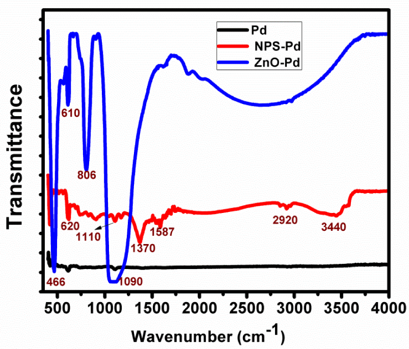
Shows the FTIR spectra of the pure Pd film, the Pd over nanoporous film and the Pd over ZnO film
Table S1 provides some information regarding the crystalline size and strains of the Pd-coated ZnO, Pd-coated NPO and normal ZnO films, as calculated from the XRD plots. The proximity of the Pd crystals to the ZnO is mentioned in the table, and it can be surmised that the as-grown ZnO demonstrates the maximum lattice strain, mostly due to the growth process identified by our group in previous research [13]. The strain is reduced significantly via Pd-coating, as the oxygen defects on the surface of the ZnO crystal causing the characteristic lattice strain are submerged in the Pd layer and also form a bind in terms of Pd-O-Zn on the surface of the ZnO lattice.
3.2 Gas sensing characterization
The supplementary figure S1 reports the schematic of the sensing set-up. The responses of the Pd-coated nanoporous films at temperature values of 100, 150, 200, 250 and 300°C are recorded in the presence of hydrogen and nitrogen gases, respectively (figure 6 (a)). The maximum sensitivity is found to be ∼20% at 200°C. The sensing elements are tested for different concentration values of 500, 200, 100, 50 and 20 ppm at this optimized temperature. The responses of the films indicate the reversible adsorption/desorption kinetics. The readable sensitivity (0.05% hydrogen gas) shows a detection limit of 100 ppm with the Pd-coated nanoporous films (figure 6(b)). The sensing characterization of the ZnO film is performed in a similar manner to that for the previous film, optimizing the operation temperature at a concentration of 500 ppm and identifying the optimized temperature. Maximum sensitivity is found to be 42%, corresponding to a temperature of 350°C. Figures 6 (c) and (d) show the variation in temperature and concentration, respectively. These films are found to detect a minimum concentration of 20 ppm. To increase the specificity and sensitivity of the sensing element the vertically growing ZnO structures are sputter-coated with a thin layer of Pd, as detailed above. We characterize the Pd-coated nanostructured film by exposing it to H2 in the gas sensing set-up at different temperatures, varying between 100°C and ∼300°C. Figures 6 (e) and (f) show the percentage change in resistance of the Pd-sputtered ZnO film with 500 ppm H2 at various temperatures, as well as the dynamic sensing characteristics of the sensing element. The resistance of this film is found to increase when exposed to H2 gas and falls towards the base value when the H2 supply is cut off, although a resistance gain is observed with changed concentrations of the hydrogen. The cycle depicts the adsorption/desorption phenomena of hydrogen in the ZnO lattice structure as the resistance shifts upward from the baseline, similar to the trend shown by ZnO. In a similar manner, the operational temperature for the film is found to be 200°C (refer to figure 6(e)). Figure 6(f) shows the variation in resistance with time as a function of concentration, at 50, 100, 200 and 500 ppm, respectively, at an optimized temperature of 200°C. The highest sensitivity in the vertical structures coated with Pd is found to be ∼70%, which is much higher than that obtained for the porous organosilicate film (∼20% peak sensitivity) or the ZnO film without Pd deposition (∼40% peak sensitivity). A response time of approximately 90 seconds and a recovery time of ∼97 seconds is observed in the Pd-coated nanostructures, which is less than that for the Pd-coated porous film (response time of ∼190 seconds and recovery time of ∼150 seconds) and the pure ZnO film (response time of ∼110 seconds and recovery time of ∼100 seconds). The lower response and recovery time is mostly attributed to the vertically grown nanostructures, which leave many gaps in between providing a better gas diffusivity, promoting rapid adsorption/desorption phenomena.

(a) shows the sensitivity value taken at 500 ppm for different temperature values; (b) shows the sensing plot for Pd sputtered over NPS films at 150°C; (c) shows the resistance change over time at different temperature values: 200, 250, 300, 350°C; (d) shows the resistance change over time at different hydrogen concentration: 500, 200, 100, 50, 20 ppm; (e) shows the sensitivity calculations at different temperatures and reports the maximum sensitivity of the studied films at a concentration of 500 ppm and a temperature of 200°C; (f) shows the variation in resistance over time, at an optimized temperature of 200°C, as a function of changing concentrations: 50, 100, 200, 500 ppm.
Figure 6 (e) shows the sensitivity calculations at different temperatures and reports the maximum sensitivity of these films at a concentration of 500 ppm at a temperature of 200°C. An explanation commonly provided in the literature for the changing resistance of pure palladium films is that the hydrogen, having a high bind dissociation energy (436 kJ/mole), readily dissociates in presence of Pd and gets adsorbed into the octahedral spaces in the FCC crystals. A considerable lattice distortion is thus seen, which becomes a reason for increasing the film resistance. The H2 adsorption is observed to be a reversible process. When the gas supply is switched off, the partial pressure of H2 over Pd decreases and desorption phenomena immediately take place. The phenomena cause the release of entrapped hydrogen molecules from the FCC crystal lattice, thereby decreasing resistance towards the base value. Additionally, the sensitivity of the film increases as the operational temperature is increased. Figure 7 offers a relative comparison of the variation in sensitivity of all three different sensing elements as a function of temperature. As can be seen in all three cases, there is a critical temperature for which sensitivity is the highest. Further, it can be seen that the maximum sensitivity is recorded in the case of the Pd-coated vertical ZnO structures, followed by the pure ZnO film and lastly the Pd-coated nanoporous organosilicate film. The sensitivity of the Pd-coated ZnO vertical structures is dependent on the combined effect of operating temperature and H2 concentration. For a quick response, the electron exchange must be quick so that equilibrium is established during the measurement. Because the Pd/nanowire interface is very small, a thin adsorbed H2 layer is formed swiftly at the interface, which is self-blocking due to diffusion limitations and stops the electron exchange process continuing as the hydrogen concentration is increased, resulting in quick equilibration. As the temperature is lower than the critical temperature, the electron exchange process is not fully established because the bond dissociation process of the hydrogen is critically dependent on the operational temperature. As the temperature increases further, the adsorbed hydrogen layer on the Pd/nanowire interface is suddenly depleted because the kinetic energy of the molecules resulting in bond vibrations increases the desorption rate. Enhanced sensitivity following Pd coating of the ZnO film is due to the increase in depletion layer formation (as shown in figure 8), due in turn to electronic and chemical sensitization of the film.
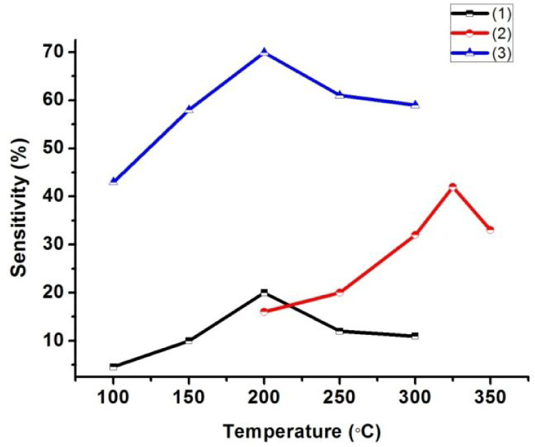
Shows the comparison between the sensitivities obtained for the different sensing platforms fabricated: (1) the Pd-coated porous organosilicate film, (2) the ZnO nano-forest over porous organosilicate film, and (3) the Pd-coated ZnO nano-forest

(a) shows the schematic of the Pd-ZnO nanowire forming a depletion layer, and figure 8(b) shows the energy band diagram of the metalsemiconductor interface. ΦB represents the metal work function, Xs is the electron affinity of the semiconductor, Ec is the lowest conduction band, Ev is the valence band, Vd is the diffusion potential, Ef represents the Fermi level and Uo represents the vacuum level.
Oxygen species, being highly reactive among the atmospheric gases, trap electrons from ZnO. Since electron density in the bulk is altered by this process, a depletion layer is developed and band bending occurs. At higher temperatures, oxygen molecules can weakly bond to the catalytic Pd atoms [51] and the oxygen atom is produced in a complex dissociation reaction. This oxygen atom finally becomes a negatively charged oxygen ion by trapping an electron from the surface of ZnO.


Meanwhile, due to the PdO attached to the surface of ZnO, a heterojunction at the interface between ZnO (n-type semiconductor) and PdO (p-type semiconductor) will be formed. The heterojunction leads to band bending in the depletion layers [52]. The electrons transfer from the n-type ZnO to the p-type PdO, while the holes transfer from PdO to ZnO until the system reaches equilibrium. These charge transfers lead to a wider depletion layer and greater resistance. As the reaction proceeds, the electrons pass through the depletion layers of the heterojunction under certain high temperatures, which once again thins the depletion layer at the PdO/ZnO interface, facilitating greater electron transport between PdO and ZnO and, as a result, the response-recovery times and optimum operating temperature of the sensor decrease significantly, as compared to its undecorated counterpart. Thus we can conclude that, in Pd-functionalized sensing films, hydrogen diffuses to the Pd-ZnO interface and causes the observed variation in work function that is consequently responsible for higher sensitivity.
Theoretical estimation of gas sensor response to different hydrogen gas concentrations is then performed. Response time is defined as the time required for the sensor to respond to a step concentration change from zero to a given concentration value). The sensor response is fitted to first-order exponential functions with the following equation:


where R0 is the initial resistance of the sensor in air, t1 is the time at which the target gas is turned off and t2 is the time at which the sensor recovers its original value. τ1 and τ2 are the time constants for the response and recovery steps, which are calculated by first-order fitting. The time constant is defined as the time required for the gas sensor to reach 63% of its original value.
The Pd-coated vertical nanostructures show a steep change in time constant with a miniscule concentration of hydrogen due to a rapid electron exchange and faster adsorption/desorption kinetics. This is not the same as the pure ZnO vertical nanostructures or the Pd-coated NPO films. Figure 9 presents a comparison of response time constants for various gas concentration, in which (1) depicts the Pd-coated porous organosilicate film, (2) indicates the ZnO film and (3) indicates the Pd-coated ZnO film.

Shows a comparison of response time constants with different gas concentrations. (1) indicates the Pd coated porous organosilicate film, (2) indicates the ZnO film and (3) indicates the Pd-coated ZnO film.
3.3 Selectivity test
To resolve the issue of gas sensing platform selectivity, response towards other nonspecific gases (viz., CH4 and CO2) is evaluated. It is found that Pd-coated nano-brushes provide sensitivity of 7% towards CH4 (at 500 ppm) and sensitivity of 5 1% towards CO2 (at 500 ppm). Resistance changes with respect to time are shown in figure 10 (a) and test gas responses at 500 ppm of each gas (i.e., H2, CH4 and CO2) are shown in figure 10 (b). These testing results confirm the selectively towards hydrogen gas of fabricated nanoscale gas sensing platforms
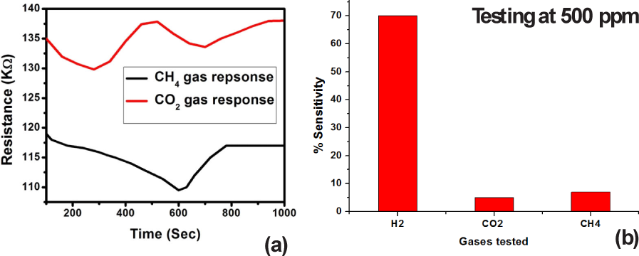
Shows the variation in resistance of the Pd-coated ZnO nano-jungle film over time. The sensitivity value found for CO2 is 5.1% and for CH4 is 7%, at 500 ppm and 200°C.
4. Conclusion
Novel sensing platforms are developed in order to explore high surface area films. A comparison of three sensing platforms (Pd/NPS/Si, ZnO/NPS/Si and Pd/ZnO/NPS/Si) is performed and Pd-coated ZnO nano-jungles are found to have higher recognition specificity, as well as better sensitivity and response/recovery times. All measurements are performed dynamically in a specially-designed gas sensing system and optimization with respect to temperature is carried out in each case. The sensitivity of the Pd-coated vertical ZnO nanostructured films is found to be ∼70%, with a response time of ∼90 seconds and a recovery time of ∼97 seconds. The films are found to be highly selective to hydrogen in the presence of CH4 and CO2 gases.
Footnotes
5. Acknowledgements
The authors are grateful to the National Program on Micro and Smart Systems (NPMASS) for financial support in performing this work. They also thank the Nano-science Centre for their help in regard to imaging and other material characterization.