
Abstract
Slanted Cu nanopillars with uniform arrays were fabricated using slanted Si channel structures as templates. A slanted plasma etching technique was employed, utilizing a Faraday cage system for the formation of these slanted channel structures. The angle of the slanted channel structures was accurately controlled because ions entering the Faraday cage maintained their direction. After the slanted channel structures were formed, they were filled with Cu by electroless deposition. Chemical mechanical polishing was then used to remove the excess Cu film and the SiO2 masks. Finally, the remaining poly Si of the channel structures was removed by wet chemical etching. This work offers a novel method for the fabrication of slanted metal nanostructures with uniform arrays covering a large area.
1. Introduction
Slanted copper (Cu) nanostructures such as nanopillars have drawn a large amount of attention due to their high thermal and electric conductivities, controllable optical properties and high mechanical strength [1-3]. They are currently used in supercapacitors, rechargeable batteries, plasmonic arrays, heat radiating modules, micro-post evaporator wicks, micro heat pipes and interconnections of ultra large scale integrated circuits (ULSI) [4-9]. In all of these applications, precise control over the angle and aspect ratio of the Cu nanopillars is of primary importance.
Currently, slanted Cu nanopillars are fabricated primarily using glancing angle deposition [10-13]. In this technique, the trajectory of an incident vapour flux is directed off-normal to the substrate and the resulting film is deposited at an oblique angle due to self-shadowing during the initial nucleation stage. While many types of metallic films can be obtained using glancing angle deposition, films deposited in this manner are usually porous. It is also difficult to obtain uniform array of pillars over a large surface area, which limits the usefulness of films deposited in this manner.
The use of slanted channel structures as templates is an attractive alternative for the fabrication of slanted Cu nanopillars. Such structures can be obtained using various methods, such as orientation-dependent wet chemical etching, ion beam etching and slanted plasma etching [14-18]. Of these methods, slanted plasma etching is advantageous for fabricating slanted patterns over a large area with excellent uniformity in pattern height and diameter, because it can be performed under practical plasma processing conditions [18].
In this study, a novel method for the fabrication of slanted Cu nanopillars is demonstrated. Slanted Cu nanopillars were fabricated onto a Si substrate using slanted channel structures as templates. These slanted channel structures were obtained using slanted plasma etching with a specially designed Faraday cage system.
2. Fabrication of slanted Cu nanopillars
Figure 1 shows a schematic diagram of the fabrication process of the slanted Cu nanopillars. The sample was a Si substrate featuring a poly Si film on a SiO2 etch stop layer. The poly Si film had hole patterns with a SiO2 mask. The slanted plasma etching process using a Faraday cage system was first conducted in order to prepare the slanted Si channel structures. The slanted channel structures were filled with Cu using electroless deposition. Then, the excess Cu film and the SiO2 masks were removed using chemical mechanical polishing (CMP). Finally, the remaining poly Si between the Cu pillars was removed using wet chemical etching, yielding the final slanted Cu nanopillars.

Schematic of the fabrication process of slanted Cu nanopillars
2.1 Slanted plasma etching
Slanted channel structures of Si were prepared using slanted plasma etching. In a conventional plasma etching process, a sheath is formed along the surface of a substrate as a consequence of the much smaller mass of electrons compared with ions. An electric field is thus established that attracts ions and repels electrons, causing ions to acquire directional energy in the sheath. Therefore, the direction of ions incident on the substrate is vertical to the surface of the substrate, regardless of the angle of the substrate (see Figure 2). It is this normal incidence of ions that results in anisotropic profiles in a conventional plasma etching [19]. Therefore, a simple method of tilting the substrate on the electrode in the plasma does not allow for control of the angle of ions incident on the substrate. This implies that conventional plasma etching is not adequate for preparing slanted etch profiles.
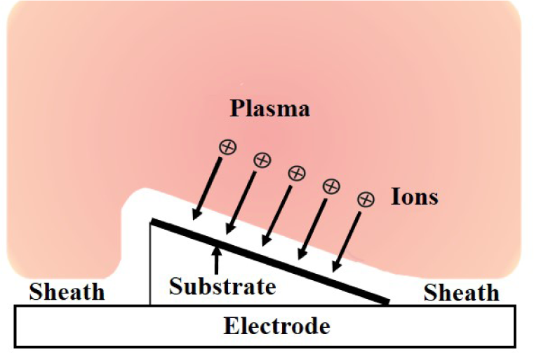
Schematic of the direction of ions incident on the inclined substrate in a conventional plasma etching process
The angle of ions incident on the substrate can instead be controlled using a so-called Faraday cage system, as shown in Figure 3. A Faraday cage is simply a closed box of a conductor. If the top plane of the cage is composed of a conductive grid and the size of the grid openings is smaller than the sheath thickness, ions will enter perpendicular to the sheath formed along the top plane. As ions transport inside the cage, they maintain their initial direction because of the uniform electric potential within the cage. Therefore, the ion-incident angle can be controlled by varying the angle of the substrate holders. Here, the ion-incident angle (θ) is defined as the angle between the direction of ion incidence and the surface normal to the substrate.
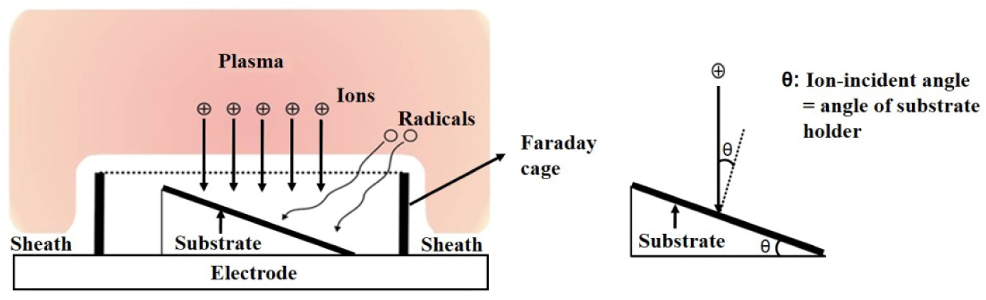
Schematic of the direction of ions incident on a substrate located in a Faraday cage. The ion-incident angle (θ) is defined as the angle between the direction of ion incidence and the surface normal to the substrate.
The slanted plasma etching process was conducted in an inductively coupled plasma chamber equipped with a Faraday cage. The Faraday cage used in this study consisted of a cylindrical stainless steel sidewall and a horizontal cover grid. The grid diameter and pitch were 0.025 and 0.229 mm, respectively. The angle of the sample holder was 15°.
Figure 4 shows a scanning electron microscopy (SEM) image of the slanted Si channel structures that were obtained using slanted plasma etching. Slanted plasma etching was performed using a cyclic process consisting of alternating etching and deposition steps. SF6 and C4F8 plasmas were used in the etching and deposition steps, respectively. The process conditions were identical to those reported previously [18]. In the etching step, the source power was 400 W, the bias voltage was −100 V and the chamber pressure was 10 mTorr. In the deposition step, the source power was 400 W, the bias voltage was 0 V and the chamber pressure was 30 mTorr. This SEM image shows that the angle of the slanted channel structures with respect to the surface normal is 15°, which correlates well to the angle of ions incident on the substrate. In addition, the slanted channel structures are highly anisotropic with fairly straight sidewalls.

SEM image of slanted channel Si structures obtained using the Faraday cage. The ion-incident angle was 15° from the surface normal.
2.2 Cu filling
Electroless deposition was carried out in order to fill the slanted channel structures with Cu. In order to initiate electroless deposition, the substrate was activated in 1 L of an aqueous solution containing 0.1 g PdCl2, 0.5 mL 50% HF and 3 mL 35% HCl for 40 s. Cu was then electrolessly deposited in a bath containing 5 mL 2,2′-dipyridyl, 5 g CuSO4 H2O, 15 g ethylenediaminetetraacetic acid (EDTA) and 5 mL paraformaldehyde (HCHO)n in a 1 L aqueous solution. The deposition was performed at a constant temperature of 85°C for 420 s. Under the electroless deposition condition used in this work, the typical deposition rate was about 230 nm/min.
Figure 5 shows an SEM image of the slanted channel structures filled with Cu. This image demonstrates that the slanted Si channel structures were filled with Cu without the formation of voids. Voids in the deposited Cu are undesirable because they result in thermal and electrical instabilities [20].

SEM image of the slanted channel structures filled with Cu
2.3 Removal of the excess Cufilm and the SiO2 masks
During electroless deposition, Cu was intentionally overdeposited in order to ensure complete filling of the channel structures. This excess Cu film, as well as the SiO2 masks, was removed using CMP performed with a polishing equipment (M-Prep 3TM, Allied High Tech) at a rotational speed of 40 rpm. An alumina slurry of 0.8 μm was used as an abrasive.
Figure 6 shows an SEM image of the Cu-filled slanted channel structures after removal of the excess Cu film and the SiO2 masks. After CMP, the thickness of poly Si is 1,006 nm, which is nearly the same as that seen in Figure 5 (1,035 nm), implying that the excess Cu film and the SiO2 masks were successfully removed.

SEM image of the Cu-filled slanted channel structures after removal of the excess Cu film and the SiO2 masks
2.4 Removal of poly Si
The remaining poly Si between the slanted Cu nanopillars was removed using wet chemical etching, conducted in 1 L of an aqueous solution containing 100 g KOH and 200 mL n-propanol. In this solution, the hydroxyl group from the n-propanol does not react with poly Si, but enhances the wettability of the poly Si surface with KOH, resulting in a uniform etch rate of poly Si [21]. The temperature of the etching solution was maintained at 85°C.
Figure 7 shows an SEM image of the slanted Cu nanopillars after removal of poly Si, which shows that uniformly arrayed slanted Cu nanopillars were successfully fabricated on the Si substrate. The diameter and height of the slanted Cu nanopillars are 360 and 1,006 nm, respectively, which are similar dimensions to those shown in Figure 5. In addition, the angles of the slanted Cu nanopillars are 15° from the surface normal, corresponding to the angle of the sample holder in the Faraday cage. It is noted that the angle of the slanted Cu nanopillars can be controlled by varying the angle of the slanted Si channel structures, which in turn can be controlled by changing the angle of the sample holder in the Faraday cage.
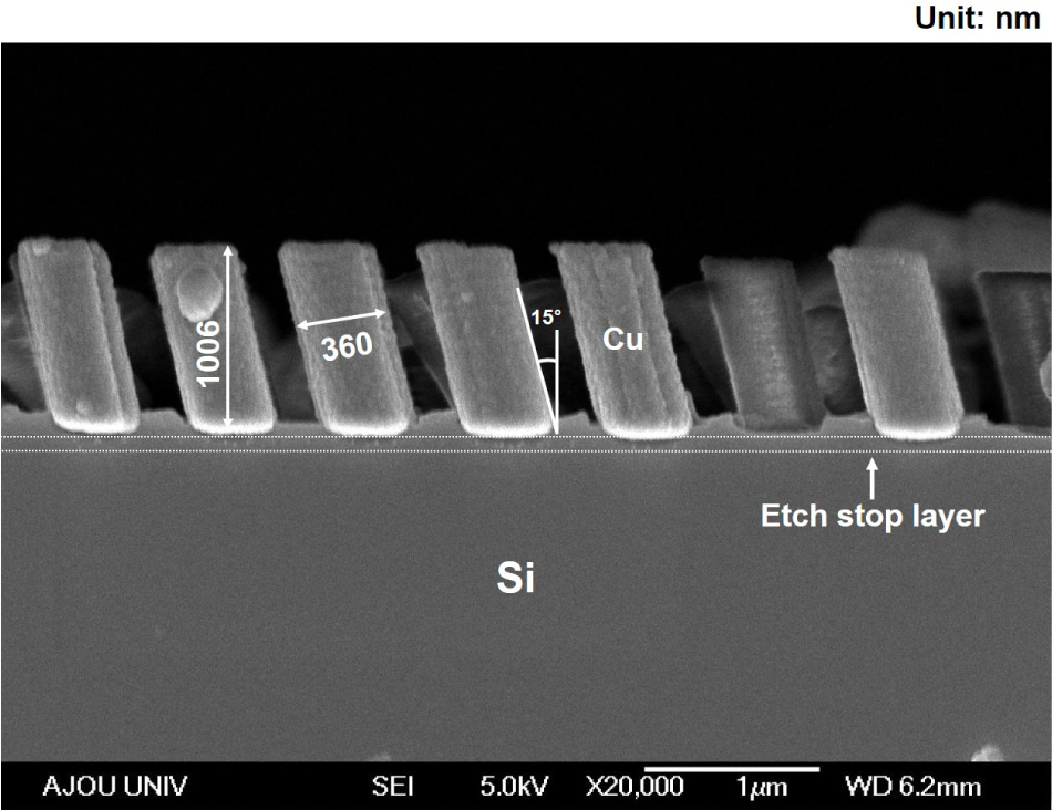
SEM image of the slanted Cu nanopillars after removal of poly Si
3. Conclusions
A novel method was presented for fabricating slanted Cu nanopillars. Uniform arrays of slanted Cu nanopillars on Si substrates were realized using slanted channel structures as templates. Slanted Si channel structures were obtained using slanted plasma etching conducted in an inductively coupled plasma chamber equipped with a specially designed Faraday cage.
Starting from the template of slanted channel structures of Si, the fabrication process consisted of Cu filling by electroless deposition, removal of the excess Cu film and the SiO2 masks using CMP and removal of the remaining poly Si by wet chemical etching. The angle, diameter and height of the slanted Cu nanopillars had excellent uniformity, suggesting that this method could also be used to fabricate uniformly arrayed slanted nanostructures of other metals.
Footnotes
4. Acknowledgements
This work was supported by the National Research Foundation of Korea (NRF) and by a grant from the Korean government (MEST) (Grant Nos. 2015R1A2A2A01002305 and NRF-2009-0094046).