
Abstract
Image feature detection and matching is a fundamental operation in image processing. As the detected and matched features are used as input data for high-level computer vision algorithms, the matching accuracy directly influences the quality of the results of the whole computer vision system. Moreover, as the algorithms are frequently used as a part of a real-time processing pipeline, the speed at which the input image data are handled is also a concern. The paper proposes an embedded system architecture for feature detection and matching. The architecture implements the FAST feature detector and the BRIEF feature descriptor and is capable of establishing key point correspondences in the input image data stream coming from either an external sensor or memory at a speed of hundreds of frames per second, so that it can cope with most demanding applications. Moreover, the proposed design is highly flexible and configurable, and facilitates the trade-off between the processing speed and programmable logic resource utilization. All the designed hardware blocks are designed to use standard, widely adopted hardware interfaces based on the AMBA AXI4 interface protocol and are connected using an underlying direct memory access (DMA) architecture, enabling bottleneck-free inter-component data transfers.
Introduction
Point correspondences found in sequences of images are the input data for a wide range of computer vision algorithms, including tracking [1, 2], 3D reconstruction [3, 4], image stitching [5], visual odometry [6, 7], video surveillance [8, 9] and simultaneous localization and mapping [10, 11]. As the quality of the input data directly influences the final results produced by the aforementioned algorithms, numerous solutions to the problem of automated image feature extraction and matching have been proposed by the research community. The most important characteristic of a quality feature detector is its repeatability. The feature should be an accurate and stable projection of a 3D point to a 2D image plane regardless of the transformations or distortions introduced by frame-to-frame camera movement. Robustness against varying acquisition parameters, like changes in illumination or noise, is also desirable. Feature matching supplements feature detection by establishing point correspondences across two or more views of the observed scene. The matching is usually performed based on some kind of descriptor that capture the distinctive characteristics of the neighbourhood of the feature. The distance between the descriptors is then used as the similarity measure. Regardless of the transformations and distortions that the feature neighbourhood undergoes, the matching method should allow reliable and robust association. As the image feature detectors and descriptors are often used as a part of a real-time image processing pipeline, the processing speed is also an important parameter of this class of algorithms. Although numerous corner detection algorithms have been proposed, none of them offer a ‘one size fits all’ solution. The performance depends to a great extent on the processed image content (type of features, contrast, noise type and characteristics in the image, etc.) and the type and magnitude of inter-frame transformations (in-plane rotations, perspective and affine distortions, scaling). Moreover, while some of the algorithms offer high-quality results, their complexity makes them too slow for real-time applications.
Goal and Motivation
In this paper, we present a complete solution for the image feature detection and matching problem. The proposed solution is based on the FAST (Features from Accelerated Segment Test) [12] and BRIEF (Binary Robust Independent Elementary Features) [13] algorithms, and is implemented as a standalone coprocessor, based on a field programmable gate array (FPGA), capable of the continuous processing of incoming image stream data. The main advantages of such a hardware-based solution are its high processing speed, relatively low power consumption, compactness and flexibility. In a typical application scenario, the proposed solution is capable of performing image feature detection, description and matching, with the speed within the range of over 100 frames per second while consuming less than five Watts of power. It can be used as a standalone system or integrated as a part of a more complex solution both in PC-centric applications and FPGA system-on-chip (SoC) custom hardware. Such characteristics make it particularly desirable in applications like mobile robotics, vision-based surveillance, driver-assistance systems and high-speed production systems.
The choice of the detection and description algorithms for the implementation was dictated by a few factors. First, the translation of the algorithms into a parallel, pipelined, systolic, resource-efficient architecture comes in a natural way. Second, the algorithms selected for implementation are not designed to be scale and rotation invariant, yet as shown in [14, 15] and [16], the FAST-BRIEF combination has the beneficial properties of good repeatability, accuracy, a high processing speed and a low memory footprint. Third, the implementation is intended for applications with no explicit requirement for robustness to abrupt scale changes or very good rotational invariance, e.g., robot navigation or tracking. Finally, the very high frame rate enabled by the hardware implementation allows for the further alleviation of sensitivity to significant viewpoint changes.
The main contributions of the presented work are:
the implementation of a complete, compact, parameterizable system for feature detection, description and matching in programmable hardware;
the use of standard, efficient interfaces based on the AMBA AXI4 protocol and DMA-based on-chip communication mechanisms that allow for seamless integration with a wide range of architectures;
the selection of a trade-off between the consumption of programmable logic resources and the processing speed, with a number of variants analysed in the paper.
Related Work
The first commonly used point image feature detectors were derived from the early work presented in [17] and were based on the analysis of the autocorrelation function of the second-order derivatives of the image [18, 19]. The detectors were usually paired with direct matching methods, e.g., the sum of squared differences, the sum of absolute differences or normalized cross-correlation of feature neighbourhoods. Further research in the field led to the development of detectors that were invariant to rotation, scale and illumination changes [20]. At the same time, feature description and matching have evolved from direct to descriptor-based methods. A prominent example of an algorithm making use of these developments is the SIFT (Scale Invariant Feature Transform) algorithm introduced in [21]. While SIFT is highly regarded for its accuracy, it is also one of the most computationally-intensive algorithms in its class. As real-time operation is a crucial requirement for a wide range of computer vision applications, further advancements resulted in the emergence of feature detection methods focusing mainly on processing speed [22, 12], as well as feature detection and description methods aimed at improving the processing speed without sacrificing robustness [23, 24]. In the latter case, the speed-up was the result of using integral images. Another major breakthrough in feature description methods was achieved with the advent of binary descriptors [13]. Binary descriptor matching is done using the Hamming distance, which can be computed very quickly using modern commodity hardware. The binary descriptor concept was widely adopted, and the solution presented in [13] was extended to achieve scale and rotation invariance as shown in [25] and [26].
Feature detection and description operations are usually performed on standard microprocessors or, less frequently, on graphics processing units. Although such hardware platforms are affordable and well established, they are not best suited for power- and size-constrained applications [27, 28]. On the other hand, the embedded and mobile microprocessors designed for use in such conditions have a limited computational throughput. This has drawn attention to alternative computational platforms, such as programmable hardware.
Early programmable logic implementations were focused mostly on the feature detection process and were based on algorithms like SUSAN (smallest univalue segment assimilating nucleus) [29] and the Harris feature detector [30]. The advent of more complex, computationally intensive methods for feature detection and the introduction of feature descriptors such as SIFT has drawn attention to implementations in dedicated hardware for possible performance gains. The hardware architecture presented in [31] can detect SIFT features on 320×240 pixel images with a speed of 30 frames per second. In [32], a significantly enhanced system for a SIFT feature and descriptor extractor is presented, capable of processing 30 VGA frames per second. Please note that the presented architectures do not perform feature matching. Similarly, the speeded up robust features (SURF) feature detector and descriptor has been a basis for many FPGA implementations. In [33], an implementation of the feature detection and descriptor extraction based on SURF is presented. The reported speed was 10 frames per second for 1024×768 resolution images. The approach presented in [34] is a modified version of [33]. The modifications are aimed at reducing resource usage but the functionality is essentially the same, although the processing speed is lower. The architecture was further developed in [35]. The system presented in [36] focuses on the development of a highly accurate feature descriptor for implementation in programmable hardware. The descriptor has the form of a ternary vector, which results in low memory usage and enables fast feature matching.
Designs implemented in programmable hardware are difficult to compare, as the dependence on the device's internal architecture and tool settings affecting the synthesis, placement and routing process have a major impact on their efficiency [37]. Moreover, most of the architectures presented in the literature are based on other algorithms, making it especially hard to directly relate to. Nevertheless, we would like to point out some of the previous work that is related to the scope of this article and highlight the characteristic features of the described solution.
The implementation of the FAST algorithm for feature detection presented in [38] was the pioneering work to the best knowledge of the authors. Since then, alternative implementations have been presented, e.g., in [39], [40] and [41]. The resource usage and performance (in terms of the processing speed) of these circuits is similar to that proposed in this article, yet some of them lack the non-maximum suppression stage. The lack of this feature is severely limiting, since without it establishing pixel-accurate feature location by finding the local maxima in the corner score function is impossible (see Section 4.1.).
The FAST and BRIEF combination for feature detection, description and matching was described in [42]. The peak performance of the circuit presented in the paper is similar to the performance of the solution described in this work using 64 matching cores. The solution was tested in FPGA and finally implemented as a CMOS application-specific integrated circuits (ASICs), and as such it is more power-efficient and can be clocked at a higher frequency (up to 200 MHz). It is worth noting that the costs associated with the development of a dedicated ASIC circuit may be prohibitive in many applications, and it lacks the flexibility and configurability of the design presented in this paper. Furthermore, the design is only capable of storing 4,000 descriptors, as it fully relies on the on-chip memory. The limited number of features and their descriptors stored for matching might be too low, especially when dealing with high-resolution images. Moreover, the feature detection part of the design also lacks the non-maximum suppression stage. An implementation of the SIFT feature detector with the BRIEF feature descriptor and a matcher in programmable logic was described in [43]. It does not compute the feature orientation and scale, thus not providing rotation and scaling invariance. This results in the use of a rather complex feature detector for tasks that could be performed with simpler, more resource-effective hardware blocks like the FAST or Harris feature detector implementations. The authors have noted, however, that they plan to extend their design as a part of future work. The variant of the presented system capable of operation at a similar speed consumes fewer resources. Moreover, the highest performance variant of our architecture achieves three times the processing speed, with even further improvements possible thanks to its scaling capability. An implementation of FAST and BRIEF in programmable hardware is presented in [44]. The design is compact but relatively slow and based on proprietary interfaces. The use of on-chip memory for image data storage severely limits its expandability. Since the article gives away only very general information on the implemented architecture, a detailed comparison is difficult to perform.
Description of the Implemented Algorithms
FAST Feature Detection
The FAST feature detector was proposed by Rosten et al. in [22] and [12]. The detector relies on the analysis of the structural properties of the key point candidates to decide whether or not they are valid, distinctive image features. The detection is based on a 7×7 pixel neighbourhood centred on the candidate point p. In order to decide whether or not the pixel p with an image intensity value of I p is a feature, the FAST detector performs a so-called segment test on a 16 pixel Bresenham circle surrounding p. The test is passed if n contiguous pixels on the Bresenham circle with the radius r around the pixel p are darker than I p − t (‘dark’ pixels) or brighter than I p + t (‘bright’ pixels), where t is a threshold value. An illustration is given in figure 1.
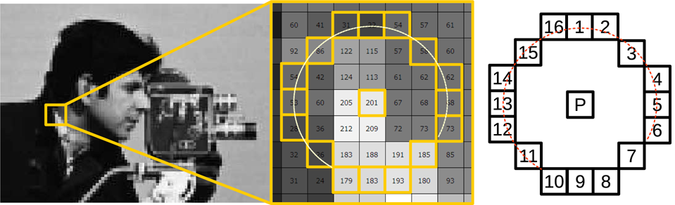
FAST image feature detector illustration. The values in the middle picture correspond to the brightness of individual pixels. Example pixels passing the segment test in the neighbourhood for a threshold value of 110 are marked with an arc.
The authors of the original solution suggest that the algorithm performs best for n=9. The way in which the segment test is formulated allows it to achieve a significant increase in speed if the individual ‘bright’ and ‘dark’ pixel tests are performed in a particular order, as many candidate points may be discarded in the early processing stage. To determine this order, the original FAST detector uses the ID3 algorithm [45] to construct a decision tree performing such a binary classification.
As the segment test returns multiple adjacent positive responses, the additional non-maximum suppression is applied to determine the stable, exact coordinates of feature points. As the segment test is a Boolean fail/pass function, the introduction of an additional corner score function is necessary. The function V is defined as the sum of absolute differences between the central point's intensity and the intensities of pixels 1–16 on the contiguous arc. A corner score for all the positive segment test responses is computed, those with V as the local maxima are retained as key points. If we denote the ‘bright’ pixels by S bright and the ‘dark’ pixels by S dark , the corner score is given by equation 1:

The concept was further developed in [46] by using a generic decision tree, which does not require learning to adapt to the target environment. The paper also includes an analysis of the influence of the pattern (the Bresenham circle) size on the detection process as well as the noise sensitivity and the effects of blur.
The BRIEF image feature descriptor proposed in [47] and extended in [13] uses binary vectors for the computation of the similarity measure based on the Hamming distance. Such a similarity measure can be efficiently calculated using modern microprocessors, making it an attractive alternative to the commonly used L1 or L2 norms.
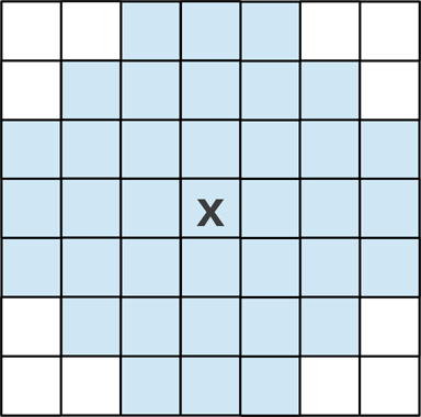
As the descriptor is highly sensitive to noise, the source image is first smoothed with an averaging filter. Each bit in the binary descriptor vector represents the result of a comparison between the intensity values of two points inside an image region centred on the feature to be described. The bit corresponding to a given point pair is set to ‘1’ if the intensity value of the first point for a given pair is higher than the intensity value of the second point, and to ‘0’ otherwise – for an illustration, see figure 2.
The authors of the original proposal evaluated several sampling strategies for the selection of point pairs. The results of the experiments led to the conclusion that sampling according to the Gaussian distribution centred on the described feature point results in the best performance. The initial smoothing was performed using a block averaging filter defined over a 9×9 mask. The descriptor length and the image patch size in which the descriptor is computed can be changed and adapted to the requirements of the application. The use of a 512 bit descriptor is suggested, but the 256 bit version performs equally well for small camera displacements and only marginally worse in other cases [47]. An example sampling pattern for a 33×33 window with 256 binary tests is presented in figure 3. The pairs of points are connected with blue lines.
As the tests performed for the computation of the descriptor are binary, BRIEF is inherently robust to illumination changes but not to rotation and scaling. However, as shown in [13], generating multiple versions of feature templates for matching may help to overcome this issue.

Formation of the BRIEF binary descriptor

Exemplary 256 point pairs for the BRIEF feature descriptor
Outline of the Architecture
Image processing algorithms can be divided into different groups based on the type of data they are working on, like pixel or region processing or methods that analyse the meta-data extracted from images. To facilitate the implementation of such a broad range of algorithms, the processing platform has to be flexible and easy to reprogram as new methods are invented and old ones are refined. The most common and natural approach is the use of standard microprocessors running computer vision software. However, computer vision methods usually require high computational power due to the vast amounts of data to be processed. At the same time, they have to be power-efficient enough to be used in power-constrained applications (e.g., robotics or smart cameras). These contradictory requirements can be eased by using a heterogeneous processing platform, like Xilinx Zynq. These devices contain FPGA logic alongside a relatively high-performance processor-based subsystem. Such a solution enables the partitioning of image processing tasks between hardware, hand-tailored coprocessors implemented in the FPGA fabric and software-based implementations that run on general purpose Cortex-A9 cores.
The system described in this paper was implemented in a Xilinx Zynq-7000 All Programmable SoC device. The block diagram of the whole solution is given in figure 4. The processor system houses two ARM Cortex-A9 cores along with an external DRAM memory controller and communication infrastructure for interfacing with the programmable logic part. The processors are used for controlling the flow of data, visualization and communication with the host computer. The programmable logic part contains a dedicated FAST detector, a BRIEF descriptor and matching coprocessors. They are connected to the memory and processor subsystem through the AXI4-Stream and the AXI4-Lite interfaces, and use DMA and specially designed controller cores. This leaves the CPUs free to use for high-level processing algorithms, operating on the matched feature set. Moreover, the use of streaming interfaces for coprocessors inputs enables the use of a wide range of image sources, such as cameras, HDMI, memory, etc.

Block diagram of the implemented system
The process of converting the software implementation of an image processing algorithm into a hardware coprocessor can be difficult and time consuming. Integrating the coprocessor with the system (e.g., external memory) and the other coprocessors is another problem that has to be dealt with. To simplify system integration, the universal controller for the streaming processors’ IP core was created. Its block diagram is given in figure 5.
This is a utility core that allows connecting streaming processors compliant with the AXI4-Stream standard to the DMA engines and controlling them by writing to their internal registers using the AXI4 system bus. It can serve as simple data feeder that adjusts communication interface data widths, handles different operating frequencies and buffers the data. It also offers some additional, subtle advantages, like an ability to fully flush the streaming core pipeline or inject some generated values into it. Another feature of the core is built-in error handling and signalling (e.g., out of the defined range, buffer over/underflow). The parameter configuration and event handling is done using a register-based interface.

The block diagram of universal controller for streaming processors
Contemporary programmable logic devices contain a pool of dual-port memory blocks for local data storage and buffering. The memory blocks can be used together with register banks to provide simultaneous access to the pixel neighbourhood in the currently processed image. Such an input block does not use the external RAM memory – which is a major advantage – as communication with external RAM can be a bottleneck in data-intensive applications. A general block diagram of the input block is given in figure 6.

The input block consisting of dual-port RAM memories and flip-flops used to organize data in a way allowing for simultaneous access to all pixels in the currently processed region
The input block operates under the assumption that the source of the image data must feed the pixels in progressive scan mode, which is common in contemporary imagers and digital video receiver integrated circuits, etc. The data stream may be continuous. On every clock cycle, one portion of the input data – a pixel intensity or a colour value – enters the circuit, and the output values of those pixels forming a rectangular image subregion are available at the outputs. Such organization of data is particularly advantageous for image processing algorithms that are local. ‘Local’ means, here, that for a region subjected to processing, the result of the computations depends only on the pixel intensity values within this region. The memory access pattern is structured and predictable. Every pixel write operation on the input causes the sliding of the whole processed region by one pixel. Writing the complete image, pixel by pixel, causes the window to slide over the whole image in a single sweep. The dual-port memory blocks can perform a read and write operation independently in a single clock cycle. Although the storage capacity of these memory blocks is relatively small, they are fast, tightly coupled with the programmable logic, and can be flexibly arranged and interconnected to form configurations with different buffer depths and data/address bit widths [48].
The main part of the described circuit is an arrangement of dual-port memory blocks, with each one of them performing the function of a first in, first out (FIFO) buffer. The depth (capacity) of each FIFO is equal to the horizontal resolution of the processed image. The width of the data bus is dependent on the image colour palette (binary, greyscale, colour, etc.) and colour depth. It is equal to the number of bits required to present complete information on a single pixel. The data flow is controlled by a simple state machine, consisting of a counter used for read and write address generation. The outputs of the FIFO memory blocks are connected to a register file. The register file is composed of programmable logic flip-flops. This facilitates independent, simultaneous access to all the pixel values.
Assuming that L is the number of memory blocks required to implement a single delay line, given the horizontal resolution of the image and the number of bits needed to represent a single pixel, constructing an architecture giving access to a region of the size of M × N (width × height) is (N − 1) L. If B is the number of bits required to store the complete information of one pixel, B ⋅ M ⋅ N flip-flops are required to implement the accompanying register file.
The circuit introduces a pipeline delay dependent on the size of the image region it generates. The delay is the time (measured in clock cycles) that elapses between writing the pixel data to the circuit and its appearance on the central element of the register file (see figure 6). If the depth of the single FIFO in the circuit is denoted by D and the size of the region implemented with the register file is M × N (width × height), the delay δ can be computed using equation 2.

Properly arranged data are fed to the input of the coprocessor, which executes the intended algorithm. If the processor is constructed in a way that enables pipelined, systolic stream processing, the resulting processing speed is very high, especially if its architecture takes full advantage of the parallel processing capabilities of programmable logic.
The block diagram of a complete system performing the detection of features using the FAST algorithm and the description and matching using the BRIEF algorithm is given in figure 7. A circuit allowing for the formation of a 7×7 pixel neighbourhood (as described in the section 5.3) is connected directly to the input of the system. In this location, the processing is split into two independent data paths – one for feature detection and one for feature description.

Block diagram of the implemented feature detection and description coprocessor (FAST with BRIEF). The numbers in square brackets denote the bit-width of the data path (e.g., [7:0] for an 8-bit connection).
Due to the specific nature of the FPGA hardware architecture, the implemented version of the FAST algorithm, although returning the same results, differs significantly from the original proposal in [22] and [12]. The original solution uses a decision tree to determine whether the pixels on the Bresenham circle fall into the ‘dark’ or ‘bright’ category. Such a concept was proposed with sequential processors in mind. The decision tree algorithm runs relatively efficiently on such hardware and allows us to discard the candidate point as a non-feature (not satisfying the ‘dark’ or ‘bright’ criteria) early on at the cost of increased memory consumption. As the presented design is based on a different computational platform, its principle of operation is also different. In place of a decision tree, an exhaustive search is performed for all the image pixels. Because the programmable logic facilitates the implementation of architectures that can perform computations in parallel, such an approach has no negative effect on the overall performance. Despite using a brute force approach for ‘bright’ and ‘dark’ pixel classifications and the corner score computation, the coprocessor consumes only a small portion of the available programmable logic resources.

Schematic diagram of the bright/dark classifier block
After the pixels have been organized into a 7×7 neighbourhood, providing access to the central pixel (the centre in figure 7) and the Bresenham circle (pixel_01 to pixel_16 in figure 7) used by FAST, the intensity values of these 17 specific pixels are passed to the inputs of the bright/dark classifier block. A schematic diagram of this functional block of the circuit is shown in figure 8.
The block consists of two independent data paths comprising a set of subtracters, comparators and multiplexers. The data paths are used to classify the 16 pixels on the Bresenham circle as either ‘bright’ or ‘dark', respectively. The input data are the centre signal and the pixel_XX signals corresponding to the central pixel intensity value and the 16 Bresenham circle pixel intensity values and the threshold value corresponding to the FAST detector threshold. The ‘bright’ data path begins with the computation of the differences between the intensity values of the pixels on the Bresenham circle and the intensity value of the central pixel. This is done using 16 subtracters. In the next step, the threshold value is deducted from the 16 results using another set of 16 subtracters. The ‘dark’ classification starts with the computation of the differences between the intensity value of the central pixel and the intensity values of the pixels on the Bresenham circle. Again, 16 subtracters are used to perform these operations. In the following step, the threshold value is subtracted from the results obtained in the previous stage. The results produced in both data paths are then fed into comparators. If the results are greater than zero, they are passed to the next processing stages to contribute to the corner score computation process as a sc_part_XX_YY signal, where XX is a number within the range of 1–16 (one for each pixel in the Bresenham circle) and YY is br for the ‘bright pixels or dk for the ‘dark’ pixels. This is achieved using multiplexers controlled by the result of comparison, as shown in figure 8. Furthermore, the results returned by the comparators set the corresponding bit in the is_bright or is_dark vector to confirm the meeting of the ‘bright’ or ‘dark’ test criteria, respectively. If the resulting value is negative or equal to zero, its value is set to zero. Moreover, the corresponding bit in the is_bright or is_dark vector is reset.
The final outputs of the classifier block are, therefore, two sets of 16 8-bit values used for the computation of the corner score according to equation 1 and two 16-bit binary vectors holding the results of the classification of the pixels on the Bresenham circle as either ‘dark’ or ‘bright’ used in the next stages to perform the segment test.
These outputs are connected to two other functional blocks. The first block is used for the corner score computation. The block consists of two pipelined adder trees. Each adder tree has 16 inputs for the corner score components from either the ‘bright’ or the ‘dark’ group of pixels. The adders produce two values – the sum of the components for both of the aforementioned groups – and the greater of those values is passed as the final value of the corner score function as per equation 1. The second module performs the segment test for both the ‘dark’ and ‘bright’ pixels, looking for at least nine consecutive logical ‘1's in the contents of the 16-bit is_bright and is_dark vectors. The block consists of two groups of 16 nine-input AND gates. If any two vectors contains a train of at least nine consecutive logical ‘1's, the result of the segment test is recognized as positive.
The resulting corner score values score and segment test results is_corner are passed to the circuit composed of FIFO memories and a register bank to form a 7×7 neighbourhood, arranging them for the subsequent non-maximum suppression. The arrangement allows us to perform all 48 comparison operations in parallel, in a single step. The points coincident with the local maximum of the corner score function in a 7×7 neighbourhood which additionally satisfy the segment test are the final resultant features.
The detector part has been enhanced with two additional counters which keep track of the numerical image coordinates of the detected features. Such functionality is necessary, as the image detector data path only puts a mark whenever it detects a feature. The first counter reflects the image column number, while the second stands for the image row number. As the raw data from the counters is out of sync with the output of the feature detector, additional delay lines have been added so that the detected features are in sync with the information of their respective coordinates. The coordinates are passed to the coordinate's intermediate FIFO buffer.
The data path for feature description begins with the averaging filter block. The original implementation of BRIEF uses an averaging filter with a square-shaped mask [47]. The motivation behind it was the fact that the response of such a filter can be computed relatively quickly on a standard PC using integral images [49]. As the hardware platform used to implement the described system is capable of massively parallel operations, a decision was made to use an averaging filter with a circular mask instead. Such a filter has better characteristics than one using a square window, as its response is isotropic. The mask was defined on a 7×7 image patch, and its shape is depicted in figure 9. The input data are taken from the same 7×7 image patch as the input data for the FAST data path.
The shape of the averaging filter mask implemented in the system
The filtered image data are then passed further to yet another FIFO and register bank circuit, so that a complete 33×33 pixel window is available for instantaneous processing. The sampling pattern used by the described architecture is the same as that given in figure 3. As the target descriptor length is 256, 256 parallel comparators are used to compute the complete descriptor in a single clock cycle. The resulting binary vector is stored in a 256-bit register. The block diagram of the module for the BRIEF descriptor computation is given in figure 10. The output of the register holding the computed descriptor is connected to the descriptor's intermediate FIFO.
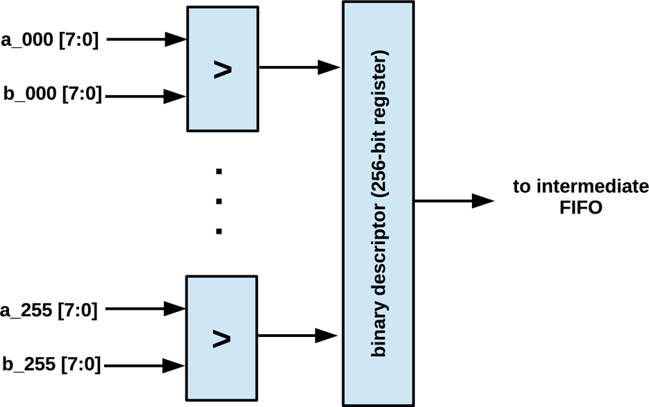
The block diagram of the module for the BRIEF descriptor's computation
The system output consists of two independent intermediate FIFOs – one holds the feature coordinates and one is dedicated to the descriptor storage. Such a solution was adopted because there is a significant difference between delays of the detector and descriptor data paths. The implementation of a spacious buffer for the coordinate storage is still less resource-consuming for synchronization than a solution in which the coordinate data are delayed alongside the data path for descriptor computation. The signal indicating the detection of the feature is used as the write-enable signal for both of the intermediate FIFOs. The signal is distributed through digital delay lines, which ensure the necessary synchronization – the coordinates and the descriptor written into intermediate FIFOs are properly aligned. As the indicator signal is only a single bit, it can be delayed with a minimum FPGA resource cost.
At the receiver side, the presence of data is signalled by the descriptor's intermediate FIFO. As this FIFO is located in the data path with longer delay, the corresponding coordinates can be read from the coordinate's intermediate FIFO without the risk of buffer underflow.
As the intermediate buffers are composed of internal dual-port memory blocks, their inputs and outputs are capable of working independently. This applies both to the clocks and the data/address lines. Such a solution enables the safe crossing of clock domains and the flexible adaptation of the circuits to different processing speeds. The ability to configure the ports on the receiver side gives the possibility of trouble-free operations with a range of receivers.
The coprocessor takes full advantage of spatial and temporal parallelism. The architecture is systolic and capable of operating on a continuous stream of data, resulting in very high performance. Additional output buffering further increases the reliability of communication.
The feature matching coprocessor is a streaming core attached to an instance of the universal controller described in Section 5.2. The coprocessor consists of the common, shared control logic part and matching cores. The matching cores are capable of independent parallel operation, and so increasing their number boosts performance. The number of matching cores is limited by the capacity of the target device. The tests of the described system were performed with a maximum of 32 such cores. The block diagram of the coprocessor is given in figure 11. The input data consists of:
N pattern descriptors, where N indicates the number of matching cores;
the compare vector, namely the vector of M descriptors to be compared with the stored pattern descriptors;
the number of descriptors in the compare vector M.

The block diagram of the matching coprocessor
The operation of the coprocessor begins with receiving N pattern descriptors and storing them in the matching cores. The number of the descriptors in the compare vector M is received next. Afterwards, each matching core compares its pattern vector with each of the M descriptors in the incoming compare vector by computing their respective Hamming distance. The index and the distance for the best correspondence are updated whenever a better matching descriptor is found. The operation is finished after M such tests are performed, and each matching core holds the index and the Hamming distance of the descriptor from the compare vector that was the closest match to its stored pattern vector. The resulting data – feature correspondences – can be read from the coprocessor and the operation can be repeated until all mutual matches are found. The detailed structural diagram presenting the feature matching coprocessor is given in figure 12.
The dotted line in the diagram separates the common part and the matching part that is duplicated depending on the number of matching cores. Each matching core consists of two parts – the first is responsible for calculating the Hamming distance between the two descriptors, while the other performs the comparisons and updates the information on the best match index and its Hamming distance from the stored pattern based on the comparison results. To achieve a high processing speed, extensive pipelining is employed. The distance is computed using 256 XOR gates, and the number of bits set in the resulting 256-bit register is computed using a pipelined adder tree. The implemented counter keeps track of the index of the currently processed element from the compare vector. To equalize the delays resulting from the Hamming distance computation pipeline, the output of the counter is delayed by nine clock cycles using a FIFO. The comparator keeps track of whether or not all the elements from the compare vector were processed and sets a flag if that is the case.
All of the described modules and systems were implemented using the low-cost Zedboard evaluation board. It hosts the Xilinx Zynq-7000 SoC (XC7Z020-CLG484-1), 512 MB of DDR3 RAM, a Gigabit Ethernet port, a USB host, an HDMI output and an FMC connector. All the systems used the 100 MHz main system clock.
The presented accelerators were created in VHDL, tested and then synthesized and implemented in the Zynq device as IP cores. The AXI universal controller for the streaming processors (see Section 5.2.) was used for connection with the processor system and memory (see figure 5). For the final verification, sets of images (an example pair of images is shown in figure 13) were downloaded to the DDR RAM memory. For processing, they were sent through the DMA engine to the detection and description accelerator. The result of this operation – a set of described features from two images – was returned and written back to the DDR RAM via DMA. In the next step, they were read via DMA by the feature matching coprocessor, and the resulting feature correspondences were written back to the memory. The results generated by the implemented hardware were compared with the results of a reference software implementation based on the OpenCV library. As expected, the results were identical.

The detailed internal structure of the matching coprocessor

Images used for verification with matches drawn
Number of frames that the FAST detector/BRIEF descriptor accelerator can process in one second for different image resolutions
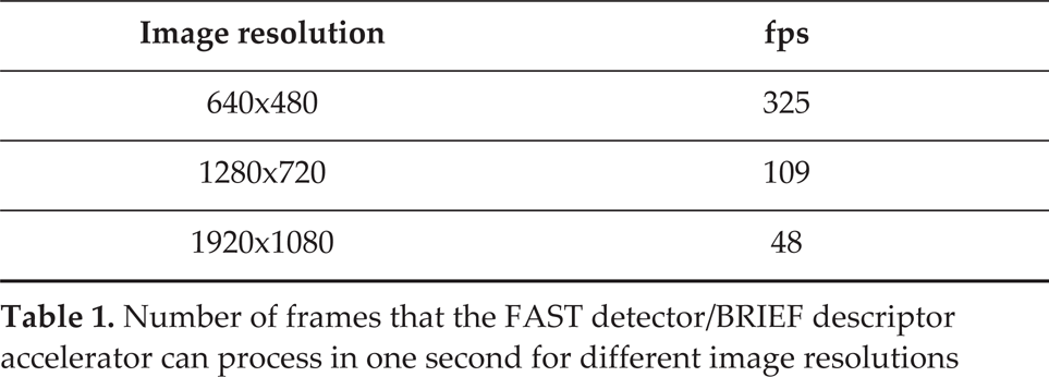
In table 2, the number of frames per second that can be processed by the detection-description coprocessor clocked at 100 MHz is given. Tests for VGA, HD and FullHD resolution images were performed. As the detection and matching coprocessor is a fully systolic functional block employing a very long pipeline, the computation time does not change with the number of features and is linearly dependent on the number of pixels to process.
The matching procedure is performed in parallel with the detection and description procedure – the features from the previous image are matched while the detection and description are performed on the next incoming image. Such a solution works best when the processing times of both parts are similar. As the detection and description time are constant for a given image resolution and system clock, only the matching procedure processing speed can be fine-tuned. This can be achieved by changing the number of matching cores to the matching coprocessor. However, as the number of matching cores increases, so does the programmable logic resource utilization. Based on the type of performed task and the performance required, the maximum number of features can be estimated and an appropriate number of matching cores can be selected.
Number of frames that each matching accelerator can process in one second for a different number of matching cores and 512 features

In table 2, the relationship between the number of matching cores and the processing speed is given. The same data are also plotted in figure 14. As shown in the figure, increasing the number of matching cores results in a linear increase of the number of frames per second that can be processed, assuming that the number of features remains constant. However, it should be noted that the speed of matching procedure is affected by the number of features. The relationship is illustrated by table 3 and figure 15. For reference, the processing speed of a software implementation presented in [13] is also given in the table. For both the software and the hardware implementation, the processing speed of the matching is inversely proportional to the number of features squared. However, in the case of the presented solution the feature description is performed independently in parallel, while the software approach is sequential by nature. The last two columns of table 3 present the increase in speed achieved using the hardware approach with regard to the software approach. The hardware accelerator with 32 matching cores is approximately 4–16 times faster than the software implementation on processors with a specialized bit-counting instruction (POPCNT on the ×86 Intel Core processor family) and 15–25 times faster on those without. It should be noted that the presented matching coprocessor achieves a relatively high processing speed even with a low number of matching cores. It can be useful in systems with more than one video input. In such a case, two or more instances of the detector-descriptor modules serve as input data sources and a high-performance matching accelerator can be shared between multiple video inputs. Such an approach is advantageous, as it allows us to reduce the load on the DMA and the use of programmable logic resources, as only one read/write channel is needed. Since the feature detection and matching operation is usually followed by other processing stages, completing this task as quickly as possible might leave more time for high-level processing. If the performance requirements are not critical, the clock frequency can be reduced to lower the power consumption.
Number of frames that the description and matching accelerator can process in one second for different numbers of features and 32 matching cores compared to a pure software implementation (tested on Core i7)

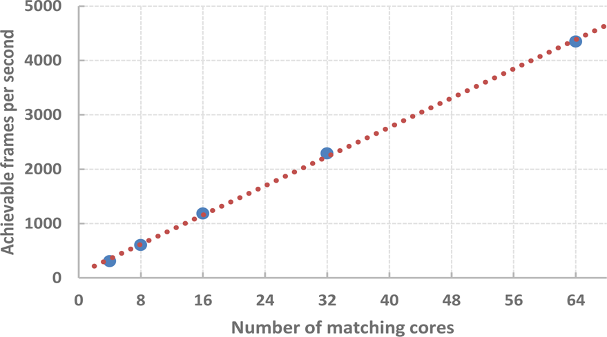
Achievable frames per second based on the number of matching cores for 512 features
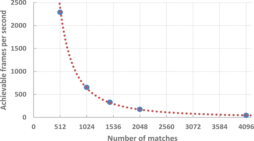
Achievable frames per second based on the number of features for a 32-core matching coprocessor
The resource usage for each module and the whole system with different numbers of matching cores is given in table 4. For easier analysis, the table contains the summary for a few variants of the design as well as the summary for its main functional blocks (the indented items). The summary for the detection and description coprocessor encompasses its own DMA module, a width converter and an interconnect. Similarly, the summary for the matching coprocessor also includes the DMA module, a data-width converter and a memory interconnect. Additional parts of the system, including the reset module and the AXI4-Lite bus, were summed up as the rest of the system. It should be noted that the presented solution is scalable and can use as many resources as are available on the target hardware platform. In this article, systems with 4–32 matching cores were implemented.
For all the configurations, the detection and description coprocessor with the DMA and interconnect uses the same number of resources, namely 9,866 (19%) LUTs, 17,412 (16%) FFs and 38 (27%) BRAMs. In the case of the smallest system with only four matching cores, it was roughly three times the number of resources used by the feature matching coprocessor (considering LUTs and FFs). It is the other way around in the case of the biggest system with 32 matching cores, which is over twice the size of the rest of the elements of the system.
The performance of the system can be further improved by using the scatter-gather engine in the DMA module. This would allow it to avoid the costly operation of packet ordering for memory transfers. It would be especially beneficial in the case of the smaller systems, with fewer matching cores. To perform frame-to-frame feature matching, they need to perform more memory transfer operations, equal to number_of_vectors/number_of_matching_cores. This, however, would come at the cost of increasing the complexity of the DMA engine and interconnect. This in turn would result in the DMA module consuming twice as many programmable logic resources. It is also possible to use a more sophisticated and larger FPGA, like Xilinx Zynq Z-7030, Z-7045 or Z-7100. This would it allow to create an even faster solution. Thanks to their increased capacity, they could hold more matching cores and also operate with a higher clock frequency.
Resource usage of each of the parts of the implemented design and the whole system (designations: LUTs - lookup tables, FFs - flip-flops, BRAMs - block RAM memory blocks). The values in percent () are given with respect to all corresponding resources available in the XC7Z020 device.

It should be noted that the presented solution uses the standard DDR RAM memory for storing all the images and the results of operations. This enables easy access to the data for other coprocessors or ARM cores performing further processing. Another advantage is the relatively high capacity of the memory (hundreds of megabytes) and its low cost in comparison to other available solutions. In addition, the system is based on commonly used communication interfaces, like AXI4-Stream and AXI4-Lite, which eases up the process of the integration of the presented solution with other systems.
This paper presents an architecture for real-time image feature detection, description and matching implemented in programmable hardware. The presented solution is supplemented with an underlying communication infrastructure based on standard interfaces, ensuring bottleneck-free, DMA-based input and output data transfers, freeing the CPU in the SoC to perform other tasks. The architecture can be easily parametrized to meet the specific design goals by choosing a trade-off between processing speed and resource utilization. Moreover, while perfectly capable of working as a standalone solution, the design can be easily expanded or integrated as a part of a more complex system. The choice of algorithms results in a compact, high performance, low power architecture, comparing favourably with the state of the art in terms of processing speed, hardware utilization and operational characteristics.
Future work will focus on integrating the design as a part of a computer vision processing pipeline, performing a complete application starting from acquisition, through feature detection, description and matching, up to high-level processing, all integrated in a single chip. Considering the characteristic properties of the described system, possible candidates are applications in robot navigation and vision-based surveillance.
Footnotes
8.
This research was financed by the Polish National Science Centre grant funded according to the decision DEC-2011/03/N/ST6/03022, which is gratefully acknowledged.