
Abstract
The optical transmission and electric field distribution of plasmonic nanostructures dictate their performance in nano-optics and nano-biosensors. Here, we consider the use of hollow, five-pointed, star-shaped nanostructures made of Al, Ag, Au or Cu. We use simulations based on finite-difference time-domain and the discrete dipole approximation to identify the strongest plasmon resonances in these structures. In particular, we were seeking plasmon resonances within the visible part of the spectrum. The silver pentagrams exhibited the strongest such resonance, at a wavelength of about 530 nm. The visible-light resonances of Au and Cu pentagrams were relatively weaker and red-shifted by about 50 nm. The main resonances of the Al pentagrams were in the ultra-violet. All the nanostars also showed a broad, dipolar-like resonance at about 1000 nm. Surprisingly, the maximum field intensities for the visible light modes were greatest along the flanks of the stars rather than at their tips, whereas those of the dipolar-like modes in the near-infrared were greatest at the tips of the star. These findings have practical implications for sensor design. The inclusion of a conformally hollow interior is beneficial because it provides additional ‘hot spots’.
1. Introduction
Plasmon resonances in nanostructures and nanoparticles have attracted interest because they can be exploited in many interesting new applications, including optical sensing [1,2], light guiding [3], biological sensors [4,5] and in the medical domain [6]. Tuning the plasmonic properties (in particular, resonance frequency and line-width) for the desired applications is achieved by changing the nanoparticles' shape, period and material, or by changing the refractive index around the nanoparticles. In general, studies of plasmonics are focused on structures made of gold (Au) or silver (Ag) because of their favourable bulk dielectric properties [7]. Nanostructures made of these elements can support high-quality localized surface plasmon resonances (LSPRs) or long-lived surface plasmon polaritons (SPPs). Despite their popularity, however, these substances do have some disadvantages: gold nanostructures, for example, can only sustain resonances at wavelengths of light greater than 510 nm. In addition, Au is expensive while Ag nanostructures are damaged by corrosion over the course of several days' exposure to air. Finally, the LSPRs in both elements are damped by interband electronic transitions, especially at the shorter wavelengths within the visible part of the spectrum. Therefore, there has been some interest in considering other materials for LSPR applications [8-13]. Cu and Al have drawn particular attention because they share some of the physical and electronic properties of Au and Ag [14-16]. Moreover, Cu and Al are abundant and cheap materials compared to the noble metals.
The LSPRs in many different shapes of nanoparticle have been investigated, with most work to date concerned with phenomena in spheres, rods and triangles. Nevertheless, the plasmonic properties of star-shaped particles have also attracted some interest [17-24] because it is expected that they will generate regions of enhanced electric field around their perimeter. It is agreed that the attractive feature of nanostars is that they provide a greater number of locations of enhanced electric field than simpler shapes [21-24], although there is certainly an optimum number of sharp points per particle beyond which overall electric field intensity declines again [23]. Both three-dimensional [17,19,21,22,24] and two-dimensional [23,24] examples of nanostars have been studied. The interest is driven by the possibility that these shapes may have applications in surface-enhanced Raman spectroscopy [19-22,24], and as plasmonic heat sources [21,22,24] in anti-cancer therapies [28] and refractometric sensing [17,23]. Generally, the location of the maximum field enhancement in such structures is at the tips of protruberances [18,21,23,26] (the ‘lightning rod effect’), but there are also reports that, under some circumstances, the maximum field intensity will instead be found in the interstices between the tips [24].
Although star-shapes are obviously more complex than discs, rods or spheres, they can certainly be produced by focussed ion beam (FIB) milling [29], or by electron beam lithography (EBL) (Figure 1).
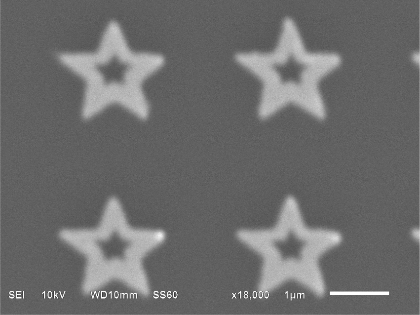
Example of five-pointed gold nanostars prepared by the authors using electron beam lithography. Other techniques such as nano-imprint lithography could also conceivably be used to produce these shapes.
Here, we explore the plasmonic properties of silver (Ag), gold (Au), copper (Cu) and aluminium (Al) using the finite-difference time-domain (FDTD) and discrete dipole approximation (DDA) methods. Our hypothesis was that the localized electric field intensity could be enhanced by providing both a star-shaped outer perimeter and a conformal, star-shaped interior cavity. A secondary aim was to determine how the material of construction would influence the local electromagnetic fields.
2. Computational Methodology
The fundamentals of the FDTD method involve solving Maxwell's equations in the time domain after replacement of the derivatives by finite differences [30, 31]. It has been applied to many problems of propagation, radiation and scattering of electromagnetic waves [32].
We used the software FDTD Solutions (a product of Lumerical Solutions, Inc., of Vancouver, Canada) to provide quantitative predictions of the localized electromagnetic field distribution as a function of wavelength of incident light. The software also provided information on other derived quantities, such as the complex Poynting vector, normalized transmission, and far-field projections. The field information can be returned in two different normalization states. Maxwell's equations can be solved in two or three dimensions, in dispersive media and some simple non-linear media, where the user can specify arbitrary geometric structures and various input excitation sources. Here, we used the three-dimensional FDTD simulator to solve TE and/or TM Maxwell's equations for infinite 2D arrays of periodically spaced nanostars. The dielectric functions at various wavelengths were obtained using Drude models [33,34] for Ag, Au, Cu and Al.
Figure 2 indicates the simulation geometry for the FDTD calculations. The array of pentagram nanostructures lay in the x-y plane. The incident light propagated along the z axis (i.e., normal incidence, θ = 0°), and the net polarization was at 45° to the x and y axes. The wavelength of light (λlight) was varied from 400 to 1200 nm. Each nanostar was 1000 nm across and 40 nm thick. In the array calculations, the centre-to-centre distance between individual nanostars was 2000 nm. The refractive index of the medium surrounding the nanostructures was 1.0 (air). (The incorporation of a glass substrate would have significantly increased the time required to do the computations, but would not have changed the overall trends and ranking.) Perfectly matched layer (PML) absorbing boundaries were used. The distance between the light source and the centre of the nanostructures was 960 nm, and 940 nm between the centre of the nanostructures and the monitor for transmission. A 2 nm mesh was used in the x-y plane. Simulation time, t (theoretically, t = Δx/2c, c is the velocity of light), was set to 125 fs.

Geometric model for FDTD simulation: (a) schematic diagram of the simulation setup; (b) pentagram nanostructures with conformally hollow interiors
Additional information on the nature of the strongest plasmon resonances in these structures was obtained by running DDA simulations on single nanostars, using the DDSCAT program designed by Draine and Flatau [39,40]. The effective radius, aeff, of the target is an important parameter in these simulations and is defined as the radius of a sphere with the same volume as that of all the dielectric materials in the target. DDSCAT provides accurate simulations of electromagnetic scattering, provided that 2πaeff/λ <25 and the dipole spacing, d, is sufficiently small that 2π d |m|/λ <1, where m is the complex refractive index [35-41]. In the present simulations, the dipole spacing was 3.3 nm, so the former parameter was of the order of 1 or 2 while the second parameter was of the order of 0.1. Results are provided as extinction, absorption and scattering efficiencies, and (after further processing using our own software) as electric field distributions as a function of phase angle (equivalent to time elapsed within a single oscillation) of the illuminating light wave.
The extinction peaks predicted by FDTD for the 2D arrays of shapes were red-shifted by about 50 nm, relative to those predicted by DDA for isolated nanostars. The deviation may be due to a combination of one or more of the following factors: (i) small differences in the intrinsic accuracy of the two computational approaches, (ii) the red-shifting effect of the neighbouring particles in the FDTD calculations, or (iii) the slightly different ways in which they handled dielectric functions (a smoothed Drude model is used in the FDTD, whereas the DDA uses a table of experimentally derived n and k).
3. Results and Discussion
3.1 Transmission Through Arrays of Pentagrams
The metallic portions of the stars cover 5.6% of the x-y plane, so the transmittance expected on the basis of simple shadowing is 0.944. Any dispersion of transmittance of light through the arrays (Figure 3) is therefore an important aspect of their optical properties, since the minima in the data suggest the wavelengths at which LSPRs might be occurring. Fig. 3 shows that there are prominent minima at λlight =550 nm (Ag), 600 nm (Au), and 610 nm (Cu). In contrast, there is no well-defined minimum for Al above the 400 nm cutoff wavelength required for the biosensor; for this reason, Al nanostars are clearly unsuitable for use in biosensing systems designed to operate in the mid-visible to near-infrared. Between λlight =680 and 900 nm, the Au, Cu and Ag arrays perform as simple, opaque dielectrics, but above that wavelength, there is evidence of another plasmon resonance (the nature of this latter resonance is examined in Section 3). It is noteworthy that the transmittance of the Ag, Au and Cu arrays is nearly identical for λlight between 700 and 1200 nm, suggesting that, for the present design of array, all three elements would produce similar operating characteristics in this range of wavelengths.

(Colour online) Transmittance of arrays of pentagram nanostructures of various materials as calculated by FDTD calculation. Inset image is the geometric model used in the simulations. The dashed horizontal line shows the transmittance expected based on simple shadowing.
3.2 Electric Field Intensity
Most biosensor schemes that exploit plasmonics rely upon a region of enhanced electric near-field to amplify and transduce the signal. Therefore, the position of such enhanced fields and their magnitude is a critical factor. In order to fully understand the optical response of our nanostructures, we carried out numerical simulations of the electric field intensity (|

(Colour online) Near-field intensity distribution in the transmission direction calculated by FDTD, when the distance between the monitor and the surface of the nanostructures is 20 nm (the position of the nanostar is outlined): (a) Ag pentagram (λlight =550 nm); (b) Au pentagram (λlight =600 nm); (c) Cu pentagram (λlight =610 nm); (d) Al pentagram (λlight =720 nm)
At the 20 nm standoff distance, the maximum value of |
The DDA technique was used to examine in greater detail the nature of the resonance, or resonances, responsible for the peak extinction. The electric field strength was evaluated on planes positioned either 3 nm above or 1 nm below the top surface of the star (Figure 5). (These locations are appropriate for situations in which the nanostars are used in SERS-type applications.) In Figure 5(a)-(c) the fields on an Ag star illuminated with 500 nm light are depicted at different phase angles (times) of the incident light wave. In this simulation, the electric field is directed along the x axis. Clearly, the resonances at 500 nm are of a relatively complex nature, with a multimodal component superimposed on a dipolar one. The same type of complex resonance is responsible for the peak extinction on the isolated Al, Au and Cu targets, at 355, 560 and 580 nm light, respectively. As shown already for the FDTD simulations, the electric field intensity for these resonances is greatest immediately above the flanks (inside and outside) of the star, and not at the sharp tips. This somewhat counter-intuitive behaviour would need to be considered when using a sensor built using an array of such shapes. The onset of these strong multimodal resonances in the nanostars is, however, broadly analogous to their appearance in other large shapes with high aspect ratios, such as nanorods [42, 43] and nano-triangles [44-46].
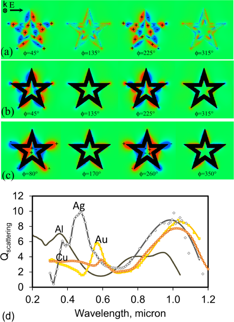
(Colour online) (a) Electric field, normal to a plane 3 nm above the surface of the silver star, generated with λlight =500 nm; (b) same as preceding but with the plane of measurement dropped to 1 nm below the top surface of the star (solid dipoles of target are rendered in black if they intersect the plane depicted); (c) same as preceding except that λlight =1050 nm; (d) Qsca coefficients for Al, Ag, Cu and Au nanostars in the above orientation
In contrast, the field developed in the resonance at λlight ≈ 1000 nm has a simpler, more dipolar symmetry, with the maximum electric field intensity at the tips of each projection. (The dipolar component can be identified from the fact that the overall charge oscillates in a left-right direction, in congruence with the direction of the electric field.) It is shown in Figure 5(c) for an Ag star on a plane that is 1 nm below the top surface of the star and can be seen to have similar peak intensity to the resonance at 500 nm. Note that, for these targets, which are relatively large compared to typical plasmonic resonators, most of the extinction is due to scattering of light rather than its absorption. The scattering cross-sections for Al, Ag, Cu and Au nanostars are shown in Figure 5(d). There is some scatter in the calculated results for Ag at the longest wavelengths, due to difficulties in converging the calculations as a result of the high value of Ag's refractive index. However, a general trend for a dipole-like resonance at about 1000 nm is clearly evident. The similarity in the intensity of resonances for these materials was also evident in the FDTD calculations for this range of wavelengths.
The asymmetric shape of the resonance peaks implies that some of them may be Fano resonances [47]. These arise from the interference between spectrally overlapping sharp and broad resonances [48,49].
The direction of polarization of the electric field within the plane of the star was also systematically examined but found to have little effect. This is because the stars have ten-fold rotational symmetry with respect to a bidirectional electric field. The two possible extremes of unique polarization within the plane of the star were designated E1 and E2. E1 is aligned with one of the 10 mirror planes of the star, while E2 is at 18° to E1. The scattering efficiencies and electric field distributions for the two orientations were very similar. As an example, the electric field distributions for the 355 nm resonance in an Al star are shown in Figure 6, at a phase angle of 60°.
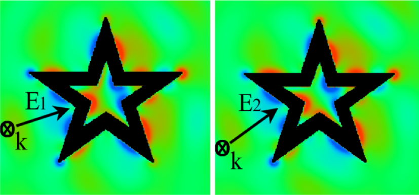
(Colour online) Effect of polarization on the electric field of the multimodal resonance in the Al star at 355 nm: (a) electric field (E1) directed along one of 10 mirror planes of star; (b) electric field (E2) at greatest possible angle (18°) from a mirror plane
4. Conclusions
Arrays of star-shaped structures of metals such as Al, Ag, Au or Cu may provide a convenient and controllable substrate for biosensors, based on surface-enhanced Raman or refractometric transduction. The dielectric function of the metal used to make the stars is a key consideration, as it controls the wavelength and intensity of any plasmon resonances on the structure. Here we have examined transmission and near-field distribution using FDTD calculations, and used DDA calculations to show that the peak extinction for the visible range of the spectrum is caused by a complex hybridization of localized multipolar resonances. The results show that Ag has the best optical properties for this type of application, but that Au and Cu are, in theory, also viable choices, albeit at slightly longer wavelengths. The near-field distribution and resonance wavelength of Cu were similar to those of Au. The wavelength at which the Al star achieved its multimodal resonance was, however, too short for convenient application in most types of biosensor. The position of maximum electric field intensity in these shapes is tunable. For visible light, there is a multimodal resonance that is maximized along the flanks of the star, whereas for near-infrared light, there is a dipole-like resonance that is maximized at the tips of the star. Due to the symmetry of the star, the direction of polarization of the light has little effect on the optical properties.