
Abstract
To maximize the utilization of its single-atom thin nature, a facile scheme to fabricate graphene multilayer films via a layer-by-layer self-assembled process was presented. The structure of multilayer films was constructed by covalently bonding graphene oxide (GO) using p-phenylenediamine (PPD) as a covalent cross-linking agent. The assembly process was confirmed to be repeatable and the structure was stable. With the π-π conjugated structure and a large number of spaces in the framework, the graphene multilayer films exhibited excellent electrochemical performance. The uniform ultrathin electrode exhibited a capacitance of 41.71 μF/cm2 at a discharge current of 0.1 μA/cm2, and displayed excellent stability of 88.9 % after 1000 charge-discharge cycles.
Keywords
1. Introduction
Supercapacitors have been regarded as an ideal candidate for energy devices, owing to their quick charge times, long life cycles and high power density [1-4]. Considering energy storage mechanisms, supercapacitors were classified into two types: electrical double layer (EDL) capacitor, and pesudocapacitor. The EDL capacitance was generated by charge adsorption at the electrode/electrolyte interface. Therefore, the structure of electrode materials is crucial for improving EDL capacitance by promoting more electrolyte ion accumulation [5]. Due to the high specific surface area, excellent electronic conductivity and electrochemical stability, carbon-based materials have been widely investigated as supercapacitor electrodes [3, 6, 7].
Graphene, a two-dimensional sp2-carbon hexagonal lattice of one-atom thickness, is one of the most attractive materials for supercapacitor electrodes owing to its large theoretical specific surface area of 2675 m2/g and high electron mobility approaching 20,000 cm2/V s[8-10]. Xia et.al [11] reported that the intrinsic capacitance of single-layer graphene is about 21 mF/cm2, implying that the theoretical electric double layer capacitance is 550 F/g. However, to date, the realized capacitance was much less than the theoretical value. The loss of capacitance was mainly caused by irreversible agglomeration and re-stacking through π-π interaction [12]. In order to utilize the surface area of each graphene layer to the largest extent, many structures were fabricated, such as curve [12] and wrinkle [13]. On the other hand, incorporating the guest materials that contain conducting polymer [14] or transition metal oxides [15], into graphene nanosheets was beneficial to prevent agglomerating or re-stacking.
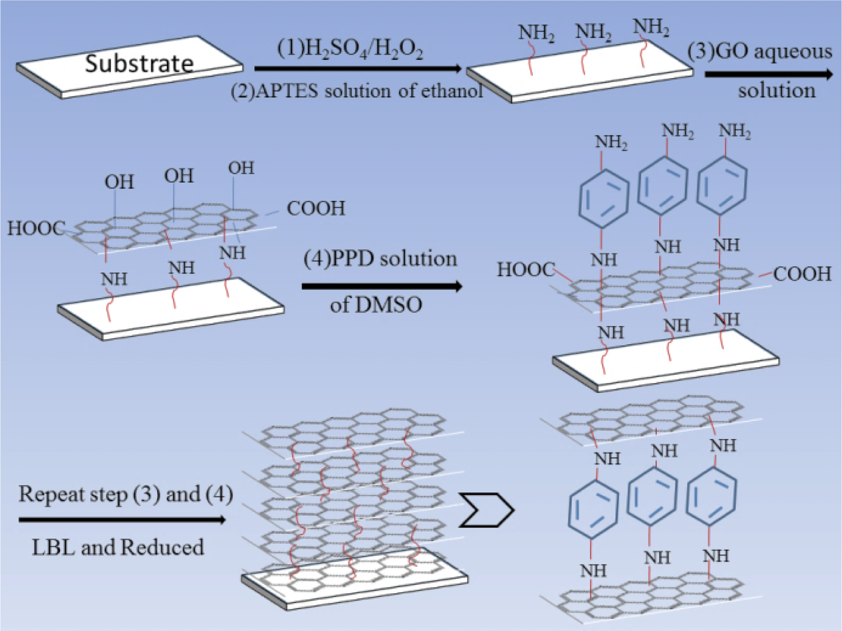
Schematic illustration of the fabrication procedure of (PPD-rGO)n multilayer films
Layer-by-layer (LBL) self-assembly, as one of most efficient techniques that could construct well-ordered lamellar nano-architectures, has attracted great attention [16-19]. Most self-assembly processes were based on electrostatic interaction, hydrogen bonds, electrochemistry, and so on [20, 21]. LBL self-assembly via covalent bonds driven by step-by-step reactions, which could achieve the preparation of robust multilayer films, has been less reported. Here, we demonstrated that ultrathin graphene films could be prepared by an LBL covalently assembled method. Utilizing the ring-opening reaction [22], the graphene oxide (GO) nanosheets were jointed with PPD as the bridge. The PPD with a benzene ring not only serves as carriers for the controllable space, but also provides a path for the electronic transmission. As a result, the uniform multilayer films exhibited excellent capacitance property and cycling stability.
2. Experimental Section
Graphite power (300 mesh, 99.95%) was supplied by the Institute of Shenghua (Changsha, China); 3-Aminopropyl triethoxysilane (ATPES, 99%) was obtained from Aladdin (Shanghai, China). All other reagents were purchased from Sinopharm Chemical Reagent Company (Shanghai, China). The substrates, silicon wafers (10×10mm2), quartz glass (10×10mm2) and indium tin oxide (ITO, 10×50mm2), were cleaned in acetone, ethanol and ultrapure water in succession, and then hydroxylated in a piranha solution (H2SO4:H2O2=7:3,v/v) at 90°C for 1 h. To maintain electronic conductivity, ITO substrates were only pre-treated in the piranha solution for 15 min at room temperature.
The thickness of multilayer films was measured using spectroscopic ellipsometry (Woollam M-2000DI, USA). The morphology images were obtained with atomic force microscopy Agilent 5500 (USA) using a tapping mode. Raman spectra were obtained from a Renishaw Invia system (UK). Fourier transform infrared spectrum (FITR) was recorded with a Thermo Nicolet 5700 spectrometer (USA). UV-Vis spectrometer Lambda800 (USA) was used to investigate the self-assembly process. X-ray photoelectron spectroscopy Thermo Escalab 250 (USA) was performed with the element and valence state. All electrochemical measurements were carried out on an electrochemical workstation CHI 660D (Shanghai Chenhua, China) with a three-electrode system in 1 M Na2SO4 electrolyte. The Pt sheet worked as the counter electrode and Ag/AgCl as the reference electrode. The working electrodes were ITO assembled with graphene multilayer films.
3. Results and Discussion
With the abundant functional groups, including epoxy, hydroxyl, and carboxyl, GO could be involved in a wide range of chemical reactions to realize its multiple functional ability [8, 23, 24]. Here, we utilized the reaction of epoxy and amidogen to assemble graphene layer-by-layer. The formation mechanism is illustrated in scheme 1. Firstly, the aminated substrates were immersed in the GO solution (0.1 mg mL−1) to produce a monolayer of graphene oxide. After ultrasonic washing to remove the absorbed graphene oxide, the composite substrates were dipped in a PPD solution of dimethyl sulphoxide, where PPD was grafted onto the GO surfaces. The substrates were then immersed in the GO solution again to produce the first bilayer of PPD-GO. The (PPD-GO)n multilayer films were obtained by repeating the previous processes. Finally, the multilayer films were treated by hydrogen iodide vapour to induce the (PPD-GO)n into (PPD-rGO)n. As shown in Figure 1a, with the number of the bilayers of PPD and GO increasing, the thickness of the (PPD-GO)n (n=1, 2, 3, 4, 5) multilayer film was linearly increased (4.0 nm, 5.5 nm, 7.1 nn, 8.6 nm and 10.1 nm) as the thickness of the first APTES/GO layer was ∼2.6 nm. The average increased thickness of the next five PPD-GO layers was ∼1.5 nm, the total thickness of GO (∼1.0 nm) and a benzene ring (∼0.5 nm). With the rigid construct of a benzene ring, the GO layers were separated an interval of 0.5 nm. As a result, these demonstrated successful layer-by-layer assembly with single-layer graphene.

(a) Plots of thickness versus bilayer number for the (PPD-GO) n ; (b) AFM image of GO, (c, d) Morphology and 3D topography (e, f) of GO layers (c, e) and GO-PPD layers (d, f)
The prepared graphene oxide was tested by atomic force microscopy (AFM). As shown in Figure 1b, the thickness of GO was approximately 1.0 nm. Importantly, the size of GO was about 2.0 μm, which was beneficial for GO assembled layer-by-layer. Figure 1c shows that the GO layers were deposited parallel to the substrates. After being dipped into the PPD solution, many nano-particles were grown on the surfaces of graphene oxide layers (Figure 1d). Initially the deposited GO film was smooth, while the entire surface later became relatively rough as shown by the 3D geography in Figure 1e and 1f, and many nano-scale spaces between graphene layers were formed. As is well known, the accessible free spaces could allow electrolyte ion storage and circulation.
The chemical structure of the multilayer film was investigated by the Raman spectrum. Figure 2 presents two prominent peaks at 1321 cm−1 and 1592 cm−1 in the (PPD-GO)5 and (PPD-rGO)5, which corresponded to the D band and G band, respectively. The D band represents the defect of sp3-hybridized, while the G band is owed to the in-plane vibration of sp2-hybridized. It could be found that the intensity ratio (ID/IG) decreases from 1.52 to 1.28 along the chemical reduction, indicating that (PPD-GO)5 was successfully reduced to (PPD-rGO)5. In particular, a small peak at 2690 cm−1, which was attributed to the 2D band, indicated that the existential state of graphene in the multilayer film was a single layer.

Raman spectra of (PPD-GO)5 and (PPD-rGO)5
To confirm the occurrence of the ring-opening reaction between GO and PPD, FTIR were recorded. Figure 3 shows that the absorption peaks at 880 and 1050 cm−1 were ascribed to the epoxy vibrations in GO. The other characteristic peaks at 1230, 1635, 1730 and 3430 cm−1 indicated that GO owned hydroxyl and carboxyl groups. In the rGO spectrum, all the peaks weakened and new peaks of 1560 and 1214 cm−1 appeared, indicating that GO was successfully reduced to rGO using hydrogen iodide vapour. After reacting with APTES or PPD, the peaks of 880 and 1050 cm−1 could not be observed, and a weak peak at 1098 cm−1 appeared that was ascribed to the generation of C-N. Therefore, it was confirmed that the epoxy groups reacted with the amidogen during the LBL assembly process. Besides, a new weaker peak was detected, which could be explained by the formation of COO-NH3+[25].

FTIR spectra of GO, rGO, PPD-GO, PPD-rGO
UV-vis absorption spectroscopy was used to monitor the assembly process. Figure 4 shows that all of the films displayed an absorption peak at 226 nm owing to the conjugated structure of GO. More importantly the intensity increased nearly linearly, indicating that GO was successfully assembled layer-by-layer and that the assembly process was repeatable. It deserves to be mentioned that the absorption peaks were basically unchanged after ultrasonic treatment for 30 minutes, demonstrating that the structure was steady.

UV-vis spectra of (PPD-GO)n (n=1,2,3,4,5) multilayer films
XPS analysis was applied to provide further confirmation of this scheme. The C1s and N1s XPS spectra of ultrathin (PPD-GO)5 and (PPD-rGO)5 films are shown in Figure 5. The (PPD-GO)5 film manifested five signals at 284.6, 285.1, 285.7, 287.1 and 289.1 eV, ascribed to the valence bonds C-C, C-N, C-O, C=O, and C(O)-O, respectively. Additionally, the N1s spectrum displayed signals of 389.9 eV (C-N) and 400.1 eV (C-NH3+). These results demonstrate the reaction of epoxy and amidogen groups. After the (PPD-GO)5 films were reduced to form (PPD-rGO)5, the signals at 285.7, 287.1 and 289.1 eV weakened, indicating that the content of hydroxyl and carboxyl groups had decreased in accordance with the FTIR spectra.
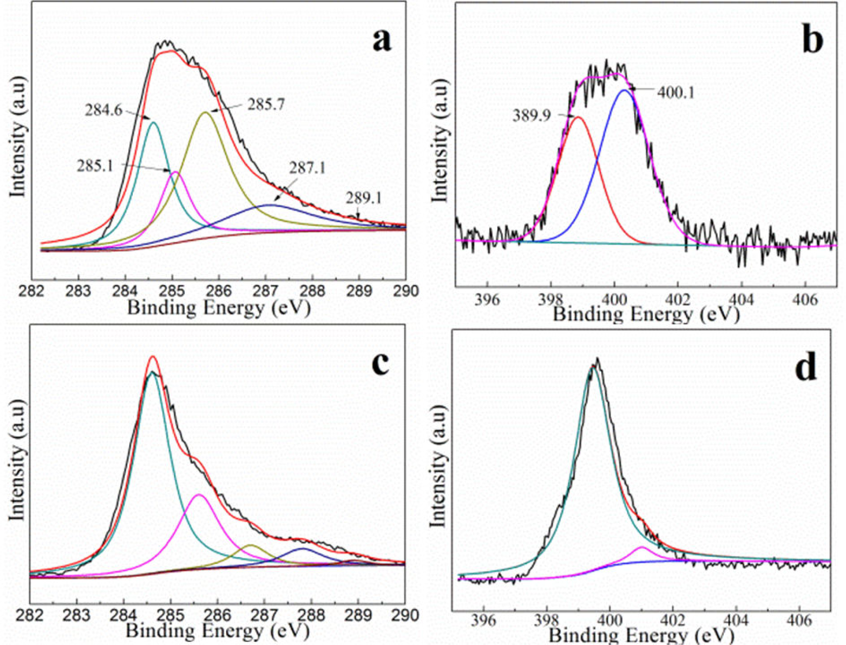
(a) C 1s and (b) N 1s spectra of PPD-GO; (c) C 1s and (d) N 1s spectra of PPD-rGO
To explore the potential application in supercapacitors, (PPD-rGO)n films were assembled on ITO to examine their electrochemical properties. The cyclic voltammetry (CV) curves of (PPD-rGO)5 are shown in Figure 6a; the nearly rectangular curves, even at a wide range of scanning rates, indicated that the multilayer graphene film possessed a favourable capacitance. The capacitances were ascribed to the combination of a double layer capacitance of graphene and the faradaic pseudocapacitance of PPD. The good charge propagation was ascribed to the spaces for ionic storage between the graphene layers.

(a) CV curves of (PPD-rGO)5 electrode at different scanning rates; (b) Charge-discharge curves of (PPD-rGO)5 electrode at different current densities; (c) Charge-discharge curves of (PPD-rGO)n (n=1,2,3,4,5) electrodes at a current density of 0.4 μA/cm2; (d) Cyclic performance of (PPD-rGO)5 electrode at 0.1 μA/cm2 for 1000 cycles
The area specific capacitance (Cs, μF/cm2) is calculated according to the following equation:

where I (μA), Δt (s) and ΔV (V) are the discharge current, discharge time and potential drop in the charge/discharge curve, respectively, and S (cm2) is the area of the active material. The representative charge-discharge curves of (PPD-rGO)5 films at different current densities are shown in Figure 6b. The curves show a symmetric triangular sharp, which indicated the ideal EDL capacitance of the graphene. The Cs at different current densities decreased slightly, demonstrating that the graphene electrodes had a good rate capability (inset of Figure 6b). The well-designed structure and abundant spaces facilitated ionic circulation. Additionally, electrical conductivity was improved due to the π-π conjugated structure. The charge-discharge curves with different numbers of layers are shown in Figure 6c, displaying that Cs increased almost linearly with the layer number. This result implied the full utilization of each deposited graphene layer.
Cycling stability is another important factor for the practical application of supercapacitors. The (PPD-rGO)5 electrode showed an excellent cycling stability with 88.9 % of the initial capacitance at 0.1 μA/cm2 after 1000 cycles (Figure 6d). This may be explained by the covalent interactions formed between the epoxy and amidogen, which were steady enough to provide a long lifetime.
4. Conclusions
In summary, a novel type of ultrathin graphene film was prepared via a layer-by-layer self-assembly method. Multilayer films assembled by covalent bonds were reproduced, and the structure was uniform and stable. With the PPD as a covalent cross-linking agent, the multilayer graphene films were assembled into an open morphology with a large layer space; the graphene therefore exhibited highly accessible surface areas. As a result, the (PPD-rGO)5 electrode performed an excellent capacitive capacity, good rate capacity and long-term cyclic stability. Finally, we believe that the success of ultrathin graphene multilayer films by the covalent self-assembly method will be useful for supercapacitors.
Footnotes
5. Acknowledgements
This work was supported by the Scientific and Technological Innovation Project of Fujian Province (Grant No. 2012H6008), Scientific and Technological Innovation Project of Fuzhou City (Grant No. 2013-G-92).