
Abstract
Ti-6Al-4V alloy with TiO2 coating is the most commonly selected material to construct an aortic heart valve. Wear resistance is the main mechanical property to be evaluated for this purpose. In this paper, the wear resistance of TiO2 thin films obtained by anodic oxidation of Ti-6Al-4V is evaluated. Anodic oxidation was performed at 20 V to 70 V with a H2SO4 1 M electrolyte. The samples were thermally treated at 500°C for 1 h, and crystalline phases of TiO2 were obtained. The wear was performed in a ball-on-flat reciprocating machine with a range of loads from 1 gf to 4 gf and times between 60 s and 1200 s, using a diamond sphere as counterface. The counterface oscillates at 0.5 Hz and 4 mm in amplitude. The wear is measured using a profilometer and is calculated as the worn volume. The wear resistance of the coated samples is larger than the substrate, and increases with thickness and with crystalline coating.
1. Introduction
Ti-6Al-4V alloy coated with a nano-film of TiO2 is a promising material to build prosthetic heart valves with good haemocompatibility properties [1-3]. Other requirements of materials in heart-implant devices are good corrosion resistance in biological fluids, mechanical resistance, and, above all, wear resistance.
The haemocompatibility of TiO2 is affected by surface roughness and crystal structure [4]. Roughness increases the total surface area in contact with blood and may promote a coagulation process [5]; it has been found that a roughness (Ra) of less than 50 nm produces only minor effects on blood compatibility [6]. The crystalline structure is also important since the dissolution of Ti ions from the rutile phase is one order of magnitude less than from the anatase phase [7]; for both it is less than from the amorphous phase [3].
One suitable method to produce oxides of uniform thickness on flat or curved surfaces is anodic oxidation [8]. The thickness of the coating can be controlled through the applied voltage between the anode (the sample) and the cathode [9]. From previous reports [10-15] it is known that films obtained by this technique produced using a 1 M H2SO4 electrolyte solution up to an applied voltage of 60 V are amorphous. In order to obtain crystalline coating a heat treatment must be applied. It has been found that a heat treatment of 1 h at 500°C produces good crystalline coating without significant changes in thickness or morphology of the films [14, 15].
Once implanted, the heart valve is under a wear regime, which is estimated to occur under a load of approximately 1 gf (gram-force).
It is known that the wear resistance of coated materials is strongly dependent on the fabrication parameters [16-18]. Besides, in films of a few of tens of nanometres in thickness the amount of wear is very difficult to measure. For that reason, the information in the literature about the wear resistance of TiO2 nano-films is scarce. The only reports are about the wear of TiO2 coating synthesized by sol-gel techniques [16-18] and about the wear of Ni-TiO2 nanocomposite films produced by electrodeposition [19]; however no studies were found about wear resistance of coatings synthesized by anodic oxidation with thickness lower than 200 nm.
In the present report anodic films of titanium dioxide were worn under a range of loads compatible with the loads expected during service of a prosthetic mechanical heart valve. The tests were performed with a ball-on-flat apparatus on crystalline and amorphous TiO2 coatings with different thicknesses, which were previously characterized [14, 15].
2. Materials and Methods
2.1 Substrate preparation
The substrates prepared for anodic oxidation were flat 10×20 mm rectangular plates of 2 mm in thickness, of Ti-6Al-4V alloy. The surfaces of the samples were mechanically polished with SiC-paper from grade #220 to #1500; then they were polished with diamond paste of 1 μm lubricated with ethylene glycol, which eliminated the typical smearing (plastic deformation) produced by the SiC particles. Finally, the surfaces of samples were chemimechanically polished with a 4:1 mix of colloidal silica (0.02 μm) and hydrogen peroxide. The final surface had a mirror finishing with an average roughness of Ra = 20 nm ± 5 nm, which was determined with a profilometer.
Before oxidation, the samples are rigorously cleaned with water and detergent in order to clean all the possible adhered particles and grease; then they are rinsed with alcohol and dried with hot air.
2.2 Coating fabrication
2.2.1 Anodic oxidation
The Ti-6Al-4V substrates, prepared as described above, were oxidized at room temperature (25°C ± 3°C) in an electrolytic cell containing a 1 M solution of H2SO4. A DC electric current was applied between a Pt cathode and the Ti-6Al-4V sample as anode, separated from each other by 5 cm. The applied voltages were 20 V, 40 V, 60 V and 70 V, held constant for a 60 s period in which the current density reduced to values lower than 2 mA/cm2. Immediately after oxidation the samples were washed with demineralized water and dried with hot air.
Two samples were oxidized at each voltage, labelled by the used voltage. One sample of each voltage was heat-treated and the other was kept untreated.
2.2.2 Heat treatment
The objective of the heat treatment was to obtain crystalline coatings [14]. One of the coated samples obtained at each voltage was heat treated in air at 500°C for 1 h. The samples were held in a furnace during heating from room temperature at a rate of 10°C/min. After one hour the samples were cooled inside the furnace. Slow heating and cooling rates have the effect of minimizing the damage which may be produced by sudden temperature changes in the coating. The samples are identified by the oxidation voltage and temperature of heat treatment, e.g. 20–500 (sample anodized at 20 V and heat treated at 500°C).
In addition, an uncoated Ti-6Al-4V substrate metallographically prepared was heat-treated at 500°C for 1 h in air, in order to compare the effect of thermal oxidation. This sample was identified as 500.
The nomenclature, thickness and crystalline structure of each sample are presented in Table 1. The thickness and crystalline structure were previously determined by X-ray reflectometry and X-ray diffraction, respectively, and published in previous works by Vera et al. [14, 15].
Thickness, structure and failure load at 60 s and performance at 300 s (1 gf load) of the films

Values calculated by extrapolation of the experimental results. The details are explained in the text.
2.3 Wear test
The wear test was performed in a ball-on-flat reciprocating machine designed and built for this purpose, and described elsewhere [14]. The wearing surface remains horizontal and static. The counterface is a diamond with conical shape with a semi-spherical tip 10 μm in radius. The tip oscillates horizontally in a straight-line path 4 mm in amplitude and with a frequency of 0.5 Hz. The load is applied by small deformations of the arm holding the diamond tip and is measured by a load cell with a precision of 0.1 gf.
The small region used for each test makes it possible to perform multiple tests on each surface. The tests were performed at several loads (1, 2, 3 and 4 gf) and duration times (30, 60, 300, 480, 600 and 1200 s).
The worn scars were observed under the optical microscope immediately after each test to evaluate the degree of wear of the coating, and, eventually, whether the substrate was completely worn through. Scanning Electron Microscopy (SEM, FEI Quanta 200) was also used to observe wear scars.
2.3.1 Measurement of the worn scar with a profilometer
The amount of wear was calculated analysing the scar profile obtained with a profilometer Time Group TR200® with a resolution of 10 nm and an RC filter (phase contrast). The shape of the scar was revealed sliding the profilometer tip perpendicular to the scar line (Figure 1).

Wear scar profiles on the sample S1-V40-T500, corresponding to the test performed at (a) 3 gf, 60 s (unbroken), (b) 4 gf, 60 s (broken)
The profile was analysed using an image processor, ImageJ [20], which permitted numerical integration of the transversal section of the scar. The process was repeatedly applied in different positions of each scar and the results were averaged.
The amount of wear was quantified as the worn volume obtained by the product of the average value of the sectional area times the scar length. The wear resistance is presented as the inverse of the worn volume. The wear measured by a change in length includes the change in length by wear as loss of material and the change in dimension due to plastic deformation; that is, the material experience wear when either of the abrasive mechanisms proposed by Kato [21] is present: wedge (the material accumulated in front of the tip) or ploughing (the material that is pushed to the side and below the tip).
3. Results and Discussion
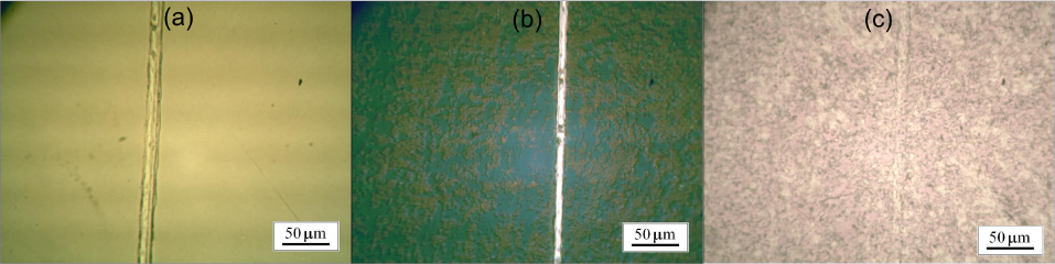
In Figure 2 we can see the appearance of the samples after each of the three main steps of the coating process, as well as the mirror-polished surface of the substrate (Figure 2.a) after anodic oxidation at 40 V (Figure 2.b) and after heat treatment (Figure 2.c).

Optical micrographs of the (a) substrate, (b) oxidized surface (40), and (c) heat-treated coating (40–500)
The first observation to be made is that the coated samples present colours directly related to the applied voltage, which in time defines the film thickness. The interference colour has been previously related to actual thickness, allowing a linear relation between thickness and applied voltage [11, 14, 15], i.e., thickness [nm] = 2.4 × voltage [V]. The effects of heat treatment on superficial properties of the coatings have been presented in previous reports [14, 15]. The main observations were that up to a voltage of 60 V the films are amorphous and above 70 V they are crystalline, presenting an anatase phase. In addition, it has been found that heat treatment at 500°C produces crystallization of the anodic film and negligible changes in film thickness. As in previous reports, it was also found that the films reproduce the roughness of the substrate ranging from 17 nm to 30 nm [15]. In Table 1 a summary of the main findings is presented.
With the aim of showing each type of scar, in Figure 3 micrographs of the different worn scars obtained at 2 gf and 60 s in three different surfaces are presented; Figure 3.a shows a polished substrate; Figure 3.b shows oxidized surface at 20 V before heat treatment; and Figure 3.c shows the surface after heat treatment (sample 60–500). The film in Figure 3.b is amorphous, thin (48 nm) and failed, leaving the substrate exposed. The film in Figure 3.c is crystalline because of heat treatment and thicker due to the larger anodizing voltage, and after wear it only suffered plastic deformation following the shape of the wear trail – it did not fail by cracking. There are two types of scars observed after the tests, shown in a larger magnification in Figure 4. Scars with broken coating and exposed substrate are shown in Figures 3.b and 4.a; scars with unbroken coatings are shown in Figures 3.c and 4.b.
Optical micrographs of worn scars in tests performed at a load of 2 gf during 60 s on (a) Ti-6Al-4V substrate, (b) 20, (c) 60–500

SEM micrographs of worn scars in sample 40–500 performed at load and time conditions that: (a) coating failed (2 gf, 60 s); (b) coating not failed by cracking (1 gf, 60 s) (the wear track is darker than the surrounding surface)
In Figures 2, 3 and 4, micrographs of anodic films with and without heat treatment reveal a homogeneous colour with a small difference in tone distributed all over the surface in small regions of the size of the grain structure of the substrate (Ti-6Al-4V, which is a bi-phase metal), indicating the effect in the film of the grain orientation of the substrate phases [14, 22].
In the analysis of wear, the effect of roughness was neglected since the coating is smooth and flat and the counterface is sharp and hard. In such cases, the main wear mechanism is abrasion. Besides, after the experiments using a load of 1 gf on a single pass it was observed that the coating deforms following the counterface profile and changing the type of contact from non-conforming to conforming; in that case the initial roughness did not have any influence in the evolution of the wear process [23, 24].
The worn volumes of nine samples as a function of load after 60 s of wear are shown in Figure 5. The set of samples includes the uncoated substrate (Ti-6Al-4V), four samples oxidized at voltages of 20 V, 40 V, 60 V and 70 V, respectively, a thermally oxidized sample (500) and three heat-treated oxidized samples (20–500, 40–500 and 60–500).

Wear maps as a function of load for a wear period of 60 s for substrate, oxidized and heat-treated samples. F indicates the load at the sample failed
The results show that the crystalline films (70, 500, 20–500, 40–500 and 60–500) present higher wear resistance than the amorphous films (20, 40, 60).
In all cases, it is observed that as the load increases the wear volume also increases. In the cases where the film does not fail in the whole range of loads from 1 gf to 4 gf, the wear volumes increase nearly linearly with applied load (sample 60–500). Moreover, the higher wear resistance of the films with respect to the substrate is clear, since there is a sudden increase of wear volume when the failure load is exceeded.
In Figure 5 it may also be observed that in some cases, for example samples 20 and 40, in which the film is thin and without heat treatment, the total wear volume is larger than the wear volume for the uncoated substrate for the same wear load, indicating a lower wear resistance of the composite (substrate and coating) with respect to the wear resistance of the uncoated substrate. In addition, the wear of sample 60 after failing at a load of 4 gf presents a wear of the order of the uncoated substrate. This may be explained by the fact that the substrate hardness is 408 HV, larger than the hardness of samples 20, 40 and 60 around 324 HV [14], which corresponds to an average hardness of the composite (substrate and coating). According to this, after the coating breaks the substrate begins to wear and the debris acts as abrasive material on the surrounding coating that still adheres to the substrate.
The effect of wear time in the wear volume for the same nine samples can be analysed using the results shown in Figure 6. All the results correspond to a load of 1 gf. The first observation is the clear difference in behaviour depending on the type of sample. On the one hand one group of samples did not fail after 300 s; this behaviour corresponded to thick samples, thicker than 140 nm (see Table 1), independent of the structure, that is, crystalline or amorphous. In this group the wear rate is constant and the lowest. The second group is identified by the fact that they fail after 300 s. In this group, in the period before failure, the wear rate is higher than in the first group, and after failure the wear rate suddenly increases.

Wear maps of nine samples showing the worn volume as a function of testing time at a load of 1 gf
The samples with the lower wear rates show the protective effect of the coating; and the fact that they wear at a constant rate without failing indicates that the protective life of the film is controlled by the thickness of the coating. The protective life, or time to failure of the film, is estimated assuming that the film fails when the depth of the scar achieves a value of 10 times the thickness of the film, as observed in samples 20, 40, 500 and 20–500, which failed. It is also assumed that the wear, as observed in Figure 6, is linear with time. With the above assumptions the times to failure estimated for the different samples that did not break during the whole test are shown in Table 1 (samples 60, 70, 40–500, 60–500). No direct relation between coating thickness and time to failure is observed; this could be explained by the fact that the intrinsic properties of the structure (amorphous or crystalline) have influence in the wear resistance, which is consistent with observations made for other films [25].
The experimental results allow us to distinguish two different wear regimes: one before and another after breaking the film. At low loads the wear of the film is moderate and after failing at higher loads the wear is severe. The transition from moderate to severe regimes is due to the applied load, which at the transition reaches a critical value – this has also been reported for other tribological systems [26, 27].
Moreover, it has been demonstrated that the film provides good protection of the substrate against wear when the applied load is below the critical, and that the wear resistance is associated with the film thickness and the degree of crystallinity.
In this respect it can be observed that a crystalline coating with a higher hardness (between 369 HV to 465 HV, increasing with rutile and voltage [14]) has a higher wear resistance than an amorphous coating for similar thickness following the Archard Law [23].
One aspect that remains to be addressed relates to the convenience or otherwise of performing accelerated wear tests for this kind of protective film, and how such results could be extrapolated into real applications. Accelerated tests are normally performed at higher than service loads, which in the present case may cause a premature failure and change the wear regime. Alternatively, an accelerated test may be performed at higher test velocities and loads below the critical for failure of a given film.
The coated samples are composite materials consisting of a ductile substrate (Ti-6Al-4V alloys) and a fragile film (TiO2); when a load is applied on this composite both materials deform, coating and substrate, until a critical pressure produces the fracture of the coating [24]. For loads producing a lower pressure in the contact zone than the critical, the wear mechanisms involved are worn by adhesion, abrasion or fatigue by contact. At higher pressures than the critical, after the coating fails, the severe wear mechanisms are abrasion and delamination.
The selection of the right coating for heart valve applications requires lubricated wear experiments. Under lubricated wear conditions a much higher resistance is to be expected than those observed under the present experimental conditions of dry wear, since the contact phenomena are strongly modified by a considerable reduction in stress concentration and temperatures in the wear zone by dissipation of heat by the lubricant [28].
4. Conclusions
The wear tests using a ball-on-flat method were performed on three different type of surfaces: (1) Ti-6Al-4V alloy; (2) oxidized samples of the same alloy producing TiO2 oxide films by anodic oxidation at different voltages and therefore different thickness between 48 and 168 nm; and (3) heat-treated substrates and heat-treated anodized samples. The main results may be summarized as follows:
Wear of Ti-6Al-4V coated with TiO2 anodic films presents two distinct regimes: one moderate at low loads, in which the film presents good resistance to wear, and another severe at higher loads above a critical value at which the film fails, exposing the substrate to higher wear rate.
The main factors providing and increasing wear resistance are films which are thicker and crystalline. In the mild regime, if the coating thickness increases, the lifetime of the coating increases linearly. In the same regime, a crystalline coating has larger resistance than an amorphous; this condition is associated to the high hardness of the crystalline coating.
The strong dependence of wear resistance on regime requires a careful analysis of wear conditions in order to predict the life of the coated material.
Footnotes
5. Acknowledgements
We wish to thank the Centro Atómico Constituyentes (Comisión Nacional de Energía Atómica), Argentina, for the scanning microscopy facilities.
We also acknowledge the financial support of the Consejo Nacional de Investigaciones Científicas y Técnicas (CONICET) and the Agencia Nacional de Promoción Científica y Tecnológica (ANPCyT) of Argentina.