
Abstract
In this work, we report on the electroplating of ultrafine and uniform magnesium (Mg) films on copper (Cu) and carbon nanotube (CNT) paper substrates. By controlling the process parameters and utilizing the pulsed deposition method, the average grain size of Mg was reduced to nano-dimensions. Surface pretreatment of the substrates by depositing a seed layer was found to be an efficient strategy for reducing the energy barrier for nucleation, thus improving nucleation density and the uniformity of deposited coatings. This work provides important guidance for the fabrication of smooth nanostructured Mg films on different substrates for a wide variety of applications.
1. Introduction
Magnesium (Mg) is the lightest structural metal [1] available for practical use. It features excellent mechanical properties including high specific tensile strength [2] and Young's modulus, excellent machinability, dimensional stability [3] and efficient vibration absorption [4]. As the eighth most abundant element in the earth's crust (2.1%), Mg is relatively inexpensive compared to other structural metals. Mg is also environmentally-friendly, biocompatible and easy to recycle [5]. All these favourable features render Mg a promising structural material for a wide range of applications, such ascomponents for high-performance vehicles [5, 6], aerospace projects [7], defence construction [8] and even medical implants [9]. On the negative side, the ductility of Mg is limited, as its close packed hexagonal (HCP) crystal structure cannot deliver interpenetrating slip systems, which are required for dislocation motion across grain boundaries [10]. Additionally, many applications demand further improvements in terms of the yield strength and stiffness of Mg and Mg alloys.
Metal matrix composites (MMCs) have been reported to show significant improvement in mechanical properties [11–13] when compared to non-reinforced monolithic metal. Several methods have been proposed for the preparation of Mg-based MMCs, including squeeze casting [14], stir casting [15] and powder metallurgy [16]. Mg-based MMCs have shown improved specific mechanical properties and low density; however, the Mg-based MMCs prepared in these reports suffer from several problems, including phase separation caused by inhomogeneous reinforced fibre distributions [17], large and uncontrolled pores inside the material and large grain size [15, 18]. Such MMCs characteristics degrade their performance as a structural material.
The Hall-Petch equation shows the relationship between the grain size of material and its yield strength and hardness:

Several methods have been explored to produce nanocrystalline or amorphous Mg. One of the most common methods is rapid solidification, which requires rapid cooling of the alloy melt to avoid crystal nucleation and growth. Several Mg alloys with small (< 1 μm) grain size have been produced by rapid solidification and powder metallurgy methods [19–23], including Mg-Cu-Y [19], Mg-Al-Ge [20], Mg-Al-Si [22], Mg-Ni-Nd [21]. However, strict requirements regarding the composition of Mg-based metallic glasses limit freedom in terms of the design of novel nanocrystalline or amorphous alloys for having the desired density and mechanical properties. Another method of producing small grains involves the severe plastic deformation [24] of metal alloys. The disadvantages of these techniques include the limited grain size obtained (commonly > 100 nm), long processing time and high energy consumption.
Electrochemical deposition allows one to control the grain size of the deposited metals by manipulating the current or voltage [25–28]. In 2002, when working toward the development of Mg rechargeable batteries, Aurbach et al. reported reversible plating-stripping [29] of Mg with ethereal electrolyte. Aurbach et al. also showed homogeneous and pure Mg deposition, which serves as a basis for the electrodeposition of Mg on various substrates. In 2007, Aurbach et al. reported “all phenyl” complex (APC) salt solutions with a wider electrochemical window and more stable performance. Direct current (DC) electrodeposition employed by Aurbach et al. is directly related to Mg battery applications, but offers limited control over the morphology and microstructure of the deposited metal layers. A too slow DC current leads to large grain size formation, while a too large current leads to electrolyte starvation and may result in the formation of very rough coatings.
In contrast, pulsed deposition [25] is a much more versatile technique. In pulsed deposition, periodical “off time” periods between current pulses allow for redistribution of the concentration profile of the electrolyte ions, which serves to homogenize the discharge current in the next “on time” period. By controlling three key parameters – pulse time, off time and current amplitude – pulsed deposition allows one to tune the properties of the deposited layer with improved accuracy.
Surprisingly, we could not find any reports on the applications of Mg electrodeposition (either DC or pulsed) for the formation of thin nanostructured Mg coatings for thin film or MMC applications. Therefore, in this paper, we were interested in investigating how manipulating key parameters of the electroplating process, including current, voltage, temperature and pulse shape, might impact the morphology and grain size of electrodeposited Mg coatings. We successfully reduced the grain size of Mg to nano-dimensions and achieved homogeneous Mg deposition on copper (Cu) and carbon nanotube (CNT) paper substrates. This work serves as an important guideline for the fabrication of nanostructured Mg films on different substrates for a wide variety of applications.
2. Experimental
Metallic Mg and Cu foil were purchased from MTI Corporation, USA. CNT paper was kindly provided by Nanocomp Technologies, USA. The electrolyte was prepared according to the previously reported procedure [30]. Briefly, aluminium chloride (AlCl3, 99.985%, Alfa Aesar, USA) was slowly added to clear tetrahydrofuran (THF, 99.9%, Novolyte, USA) and phenyl magnesium chloride (PhMgCl, 2M THF solution, Sigma Aldrich) was then added to the solution drop by drop to gain a 0.4M (PhMgCl)2-AlCl3 solution. The surface-cleaned Mg foil and selected deposition substrate (Cu or Nanocomp CNT paper) were assembled into two-electrode cells. Mg foil and the deposition substrate were separated by a 1.2 mm thick insulating polyethylene (PE) block. The central part of the PE block was removed for focused Mg electroplating in the central zone of the deposition substrate. Galvanostatic (both DC and pulsed) electrodeposition was performed with Arbin battery test stations (Arbin Instrument, BT-2143, USA). After the electrodeposition, the coin cells were dissembled in the glove box in order to collect the Mg-coated samples. The morphology of Mg deposition was characterized by scanning electron microscopy (SEM, LEO 1530, the Netherlands) operating at 8kV of the accelerating voltage and 5–6 mm of the working distance. The grain sizes of the samples prepared by different deposition procedures were characterized by X-ray diffraction (XRD, X'Pert PRO Alpha-1, USA).
3. Results and discussion
DC electrodeposition of Mg on Cu substrate was performed at 1, 4, 40 and 400 mA cm−2 current densities, with the total charge and other parameters kept constant. The deposited samples were termed as 1mA-DC, 4mA-DC, 40mA-DC and 400mA-DC, respectively. At a current density below 100 mA cm−2, uniform deposition was obtained (Figure 1). The grain size of the deposited film was found to decrease when increasing the applied current density, which was expected (compare Figure 1a,1c and 1e). Indeed, at higher current densities, less time was available for the diffusion and re-distribution of Mg atoms on the surface to form crystal grains. However, when current density exceeded 100 mA cm−2, considerable non-uniformities of the deposited film (formation of agglomerates on the surface) begin to appear. At 400 mA cm−2, we observed large-sized lumps (2–5 μm) composed of smaller metallic Mg particles (200–500 nm) (Figure 2). The very high current density led to the formation of large local electric fields near the surface (field concentration phenomenon), which, in turn, directed the incoming ion flux to specific locations. Deep cracks were found in between neighbouring lumps. This can partly be attributed to: (i) the stresses originating from the mismatch between the crystal lattices of the substrate (

SEM micrographs of Mg films DC electrodeposited on a Cu substrate at a constant current of (a-b) 1mA-DC; (c-d) 4mA-DC; and (e-f) 40mA-DC.
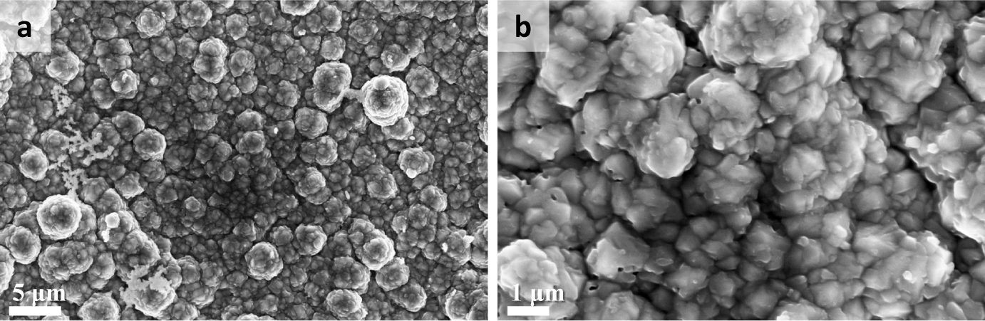
SEM micrographs of Mg film electrodeposited on a Cu substrate by constant current 400mA. Mg deposition begins to get rough at extremely high current densities such as 400mA
These results indicated that at room temperature, constant-current (galvanostatic) electrodeposition of Mg may allow for only a moderately small (∼0.5 µm) grain size to be achieved. Very high current density resulted in large porosity, large roughness, poor uniformity and overall poor quality of the Mg film, which could be detrimental to its yield strength. To achieve a more homogeneous and finer Mg deposition with smaller grains, we need to achieve we need to achieve a more uniform distribution of Mg ions in the proximity of the surface and avoid formation of electrolyte-depleted areas, where little-to-no deposition can take place.
Theoretically, upon the application of a sufficiently high current density to a DC electroplating bath, it will quickly become depleted of ions near the diffusion layer, because the charge transfer across the electrolyte-metal interface (deposition) becomes faster than the transport of metal ions through the bulk of the electrolyte. During the process of pulsed electrodeposition, ions migrated to the depleted areas in the bath during “off time” to homogenize the concentration profile. As a result, during the following “on time”, more evenly distributed ions were available for deposition. Thus, we propose a pulsed electrodeposition at high current densities but a sufficiently short pulse duration to prevent electrolyte depletion and with a sufficiently long “off time” to redistribute electrolyte and electrolyte decomposition products uniformly.
Interestingly, the length of the “off time” period was found to have a significant impact on the morphology of the deposited coating for high current density deposition. For example, Figure 3 compares the coating morphology for the 400 mA cm−2 (400mA-PD) deposition pulsed for 10 ms “on time” and 0.1s for the “off times” with the same process but an “off time” of 1s (note that the total charge was kept the same). In both samples, the grain size was very small (<200 nm) due to the high amplitude current. The longer “off time” resulted in the formation of the smallest grains (compare Figure 4d and 4b), which is a desirable outcome, but at the expense of the very high coating roughness (compare Figure 4c and 4a), which is highly undesirable for most applications. While grain size reduction for longer “off time” can be explained by a higher ionic flux across the electrolyte/metal interface (due to the longer time available for electrolyte equilibration, where more Mg2+ ions reach the proximity of the metal film and are available for deposition), the higher surface roughness or the formation of large granules was not expected.
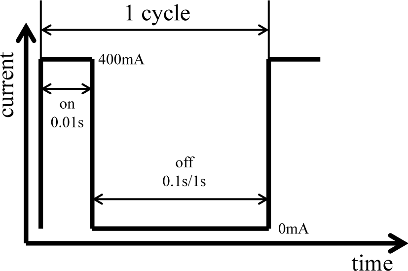
Scheme of pulsed electrodeposition

SEM micrographs of Mg film pulsed electrodeposited at “on time”=0.01s and (a-b) “off time”=0.1s; (c-d) “off time”=1s, with the amplitude of 400 mA
Because the distribution of electrolyte should have been more uniform for the 1s “off time” pulse experiments;, we postulate that the observed non-uniformities were a result of organic electrolyte decomposition products (SEI) passivating some regions of the deposited metal film. Once some initial roughness is formed, further deposition can only further amplify this roughness, because the tips of the agglomerates will concentrate the electric field in their proximity, pulling more Mg ions into their growth during each cycle. In addition, the tips of the agglomerates see higher concentration of Mg ions (similar to larger trees growing faster and preventing smaller trees from growing in the vicinity of the shade cast by taller trees). Finally, the decomposed organic component of the electrolyte may naturally accumulate in the areas of reduced growth (in the downhill areas).
Small variations in temperature were also found to significantly influence the morphology of Mg deposition. For example, Figure 5 indicates a significantly larger grain size as a result of a very moderate increase in the deposition temperature from 20 to 45 °C. The roughness of such coatings is also high.

SEM micrographs of Mg film electrodeposited on a Cu substrate by pulsed current (400mA, on time=10ms; off time=1s) at 45 °C
One of the routes for reducing the surface roughness in small-grain films is to significantly increase the number of stable nuclei formed during the Mg deposition. In this case, the field concentration phenomenon during electrodeposition at high current densities will be significantly reduced and uniform film thickness may, in principle, be attained. The nucleation density depends on multiple factors including the wetting of the metal film on the substrate, as controlled by the relationship between electrolyte/substrate, electrolyte/metal film and metal film/substrate interfacial energies. As such, metal depositions on the substrates of the same material that result in complete wetting allow one to greatly increase the initial nucleation density. Therefore, in order to deposit smooth nanostructured films on various substrates, we propose surface pretreatment of Cu (or other) substrates by seed-layer deposition, where a larger (micron-size) grain size Mg layer is initially formed. Such a layer, deposited at a low current density can be significantly more uniform, because the local electric field deviations near the substrate are smaller and more time is available for the redistribution of Mg atoms on the substrate surface. Once deposited, the seed layer allows for the formation of smooth Mg deposits at a high current density, where small grain size can be attained (Figure 6).

Schematic of (a) high current pulsed electrodeposition; (b) seed-layer assisted pulsed deposition
Figure 7 shows an example of coatings produced with a seed layer. We applied a 40 mA cm−2 pulsed deposition with 10 ms “on time” and 90 ms “off time” to deposit homogeneous Mg grains (0.5–1 μm) on Cu. The pretreatment took up 5 and 10% of the total charge in 2 different samples, respectively, shown in Figure 7a-b and 7c-d. We then applied a 400 mA cm−2 pulsed deposition to produce nanostructured Mg coatings. This step consumed the rest of the charge. In both cases, significant depression of the growth of micron-sized granules was observed (Figure 7). The deposition of a dense Mg film with very small (<50 nm) grains thus became possible. While the sample with the 5% seed layer still showed a micron-scale pattern underneath the nanoscale Mg film (Figure 7 c, d), the longer seeding time allowed for the formation of very smooth coatings (Figure 7a, b).

SEM micrographs of seed layer-assisted Mg electrodeposition on a Cu substrate: (a-b) the seed layer taking 10% of the total charge; (c-d) the seed layer taking 5% of the total charge
Formation of smooth Mg coatings on non-metal surfaces was also feasible. For example, when we utilized similar deposition parameters for Mg deposition on CNT substrate, similar nanostructured films and individual Mg nanoparticles were deposited on the sample surface (Figure 8, Figure S1). The amount of Mg deposition was characterized by EDS (Figure S2). Surface chemistry analysis by XPS confirmed the metallic state of Mg (Figure S4). For this sample, we applied a surface pretreatment with 10% charge at 40 mA cm−2, followed by pulsed deposition at the amplitude of 400 mA cm−2. The “on time” was set as 10 ms and the “off time” 1s. Nano-sized Mg nanoparticles infiltrated into (Figure S3, cross section view) and eventually uniformly coated the top surface of the CNT paper. A small number of larger Mg particles (∼200 nm) could also occasionally be seen (Figure 8). The larger size of such particles was likely the result of faster Mg growth on the surface of Fe catalyst nanoparticles present within the as-received CNT substrate.
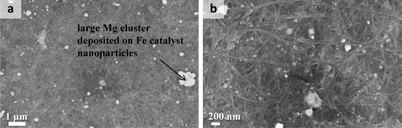
SEM micrographs of Mg coatings and nanoparticles electrodeposited on carbon nanotube paper by a pulsed current (400mA, on time=10ms; off time=1s). The fastest deposition of Mg was observed on the surface of Fe catalyst nanoparticles.
XRD characterization revealed the deposition of pure Mg on both Cu and CNT paper substrates (Figure 9). The XRD peak positions of all samples accorded well with Mg references (PDF# 65–3365). For ease of comparison, the peak intensities of Mg metal foil (bulk Mg) and 40mA-DC were reduced. The broad peak widths of the seed layer-assisted deposition samples confirmed the fine grain size of Mg deposition by seed layer assisted deposition on both types of substrates. The grains in Mg metal foil were highly oriented in the (002) direction, which was caused by the rolling process during metal foil production. Interestingly, (002) peak was diminished in the XRD profiles of Mg depositions under all conditions. Future work might focus on the fabrication and mechanical characterization of strengthened Mg-CNT composites of various densities, Mg content and porosities.

XRD spectra of Mg films deposited under selected conditions. The peak intensities of bulk-Mg and 40mA-DC are reduced for ease of comparison.
4. Conclusion
In this work, we have demonstrated the opportunity for producing smooth films of nanostructured Mg by electrodeposition. We have studied the effects of current density, pulse shape, temperature and substrate surface pretreatment on the morphology of Mg electrodeposition. High current electroplating was found to produce smaller grains within the deposited film. However, a limited number of preferred sites for nucleation, combined with a filed concentration effect resulted in the growth of large granules and as a result produced a rough Mg coating. While merely applying a pulsed electrodeposition method did not depress the formation of agglomerates, seed layer assisted pulsed electrodeposition allowed us to achieve uniform and smooth films of fine-grain Mg on Cu and CNT substrates. In addition to the applications of nanostructured Mg films as protective or functional layers on various metal substrates, this work may furthermore serve as a step towards the formation of light-weight Mg-containing composites (such as Mg-CNT) for use in a wide range of structural applications.
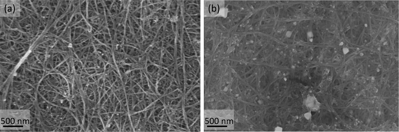
SEM micrographs of CNT substrate (a) before and (b) after Mg deposition

(a) EDS spectra of empty CNT paper and CNT with Mg deposition (40 mA cm−2 direct current deposition and 400 mA cm−2 pulsed deposition); (b) weight percentage of detected elements. Detected oxygen originates from both the adsorbed moisture and oxidation of Mg

SEM micrographs of cross section of CNT substrate (a) before and (b) after Mg deposition, showing the presence of pores in both samples. Note: some of the material may be re-deposited on the surface after being sputtered by a focused ion beam used for the SEM sample preparation.
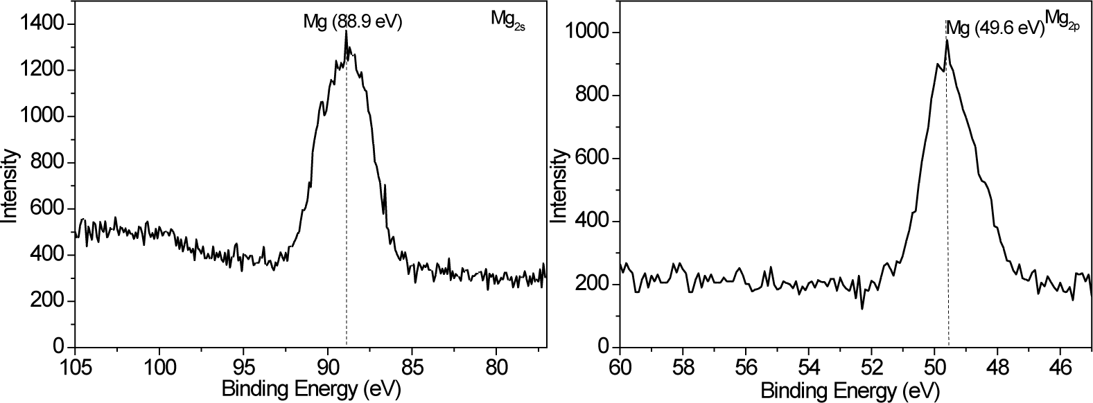
Typical high resolution Mg2s and Mg2p XPS spectra recorded from the top of the substrates and confirming metallic state of Mg
Footnotes
5. Acknowledgements
The authors wish to thank David S. Lashmore and Mark W. Schauer for their helpful discussions and Nanocomp Inc. for providing samples utilized in this project. This work was supported by the US National Science Foundation (grant 0954925).