
Abstract
Miniaturized vacuum gauges (MVGs) for the measurement range 5.7times10−7 to 1.1times10−2 mbar were fabricated in a self-aligned approach using focused ion beam (FIB) nanoma-chining and reactive ion etching (RIE). The MVG consists of two properly insulated electrodes integrated on top of an atomic force microscopy (AFM) tip, forming a coaxial embodiment. The special design enables us to vary the cathode-anode separation and the turn-on voltage changes accordingly. The experiments show that the MVGs operate at low bias potential and demonstrate very good I-P dependence over a wide pressure range.
1. Introduction
Vacuum metrology in the high and ultra-high vacuum regime plays an important role in modern industry as well as scientific research. Most common vacuum gauges used in these pressure regimes rely on ionization gauges [1, 2]. These gauges measure the electrical current resulting from the collection of the molecules ionized by electrons accelerated in high electric fields inside the gauge, which is used as an indirect measure of gas density and thus pressure [3, 4]. Device-dependent features like response time, power consumption, outgassing heat and light emission, or limited filament life time must be considered when choosing the proper vacuum gauge type for the respective application [5].
To reduce the power consumption of cold-cathode ion gauges, high-aspect-ratio cathodes were fabricated resulting in a high field-enhancement factor [6–7]. However, small fabrication variations, e.g., in emitter tip radius, height, chemical composition or crystalline orientation, can result in huge variations in emission current. Additionally, the strong electric field gradient near the cathode could cause the adsorption of gas molecules from the surroundings, thereby changing the local work function and again altering the emission efficiency.
2. Experiment
In this paper, we present an approach for the reproducible integration of an individual field-emitter device into a Si-AFM tip utilizing FIB processing and microfabrication techniques. Figure 1 shows the principle sketch and the fabrication scheme of the MVG.
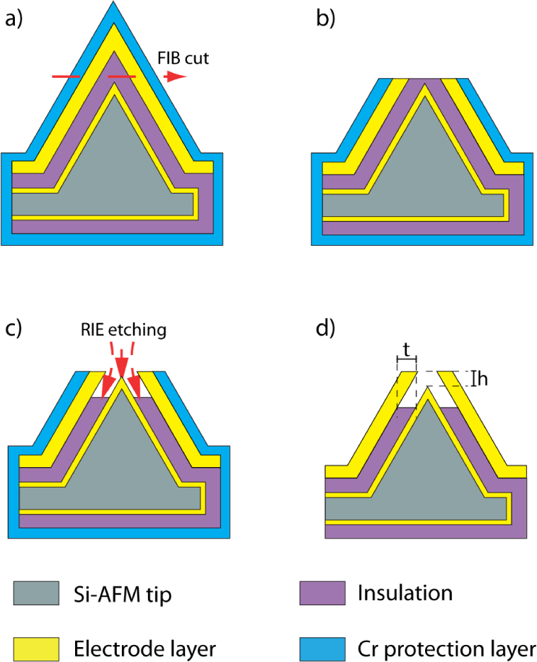
Process flow chart for MVG fabrication: (a) AFM tip with conductive Ti/Au/Ti layers, 600 nm Si3N4 and 40 nm ZrO2 as insulating layers and a 50 nm Cr protection layer; (b) tip after FIB cutting of the insulation from the apex of the tip; (c) gap formation by selective ICP-RIE etching of insulation layer; (d) fully featured MVG after the removal of the Cr layer by wet etching. Insulation thickness t and vertical anode/cathode offset h implicate the MVG geometry modulation sites, where the electrode separation is controlled by varying the insulation layer thickness or position of the FIB cutting
First, a 5 nm thick titanium (Ti) adhesion layer followed by an 80 nm thick gold (Au) and a 5 nm thick Ti layer are sputtered onto the Si-AFM cantilever. The Au layer has a later role as the field emitter (FE) - the cathode. The uppermost Ti layer provides better adhesion between the Au layer and the subsequently-deposited about 600 nm thick Si3N4 insulation layer, deposited by plasma enhanced chemical vapour deposition at 300°C. In order to improve the insulation capability, an additional 40 nm thick ZrO2 layer is deposited by atomic layer deposition.
On top of the insulation layer, another 5 nm thick Ti adhesion layer followed by an 80 nm thick Au layer are sputter deposited, later forming the ring-shaped anode around the tip. Finally, before the tip exposure by FIB cutting and RIE the probes are sputter-coated with a 50 nm thick sacrificial Cr protection layer. The final MVG blank with the completed layered structure is shown in Figure 1a. Afterwards, the Cr, Au and insulation layers are partly removed at the very apex of the tip with the FIB, utilizing a beam of Ga+ions at 30 keV and a beam current of 50 pA (Figure 1b). By careful adjustment of the FIB milling, the innermost conductive tip is kept buried underneath a Si3N4 insulation layer about 150 nm thick. Subsequently, an inductively-coupled-plasma RIE process is applied in two steps. First, a mixture of SiCl4 and SF6 is required for removal of the Ga-containing top insulation layer. Previous experiments have shown that Ga arising from the FIB processing acts as an etch-stop during Si3N4 dry etching with SF6 [8, 9]. In the subsequent RIE etching step, only SF6 is used to etch Si3N4 selectively, exposing the conductive tip, whereby the Cr layer protects the rest of the sample as shown in Figure 1c. The removal of the insulation layers results in a gap between the conical cathode tip and the surrounding ring-shaped anode. After successful electrode exposure, the protective Cr layer is removed by wet etching with Microposit chrome etch 18. Figure 2 shows the SEM image of the fully featured MVG.

SEM image of the MVG showing the Au cathode with an apex diameter of about 60 nm, surrounded by the ring-shaped Au anode with an in-between distance of roughly 640 nm
For this particular tip, the Au cathode is approximately 1μm long and has an apex diameter of about 60 nm. As indicated in Figure 1d, our MVG processing approach allows easy modulation of the MVG electrode separation by varying the insulation layer thickness (t) or the vertical anode/cathode offset (h) by tuning the position of the FIB cut.
Overall, we fabricated more than 30 devices for field emission as well as electrochemical investigations [10], demonstrating the versatility of this approach. With respect to the miniaturized vacuum gauges, we fabricated four devices with a cathode-anode spacing of about h=500 nm, and two devices with a spacing of about 1 μm. To investigate long-term stability we tested the devices for 8 h. Thereby all of this time the vacuum gauges appeared stable and the pressure dependency measurements were well reproducible.
3. Results and discussion
In order to investigate the field-emission (FE) properties and the pressure dependency, the wire-bonded MVG was glued on a chip carrier and mounted in a vacuum chamber. Once the base pressure of 5.7×10⁻⁷ mbar was reached, the emission-current characteristic was investigated as a function of the applied potential. The pressure was gradually increased, regulated dynamically by a leak valve, and for each pressure value an I-V characteristic was recorded. Figure 3 shows the pressure-dependent I-V characteristics of a MVG with a cathode-anode spacing of h1=640 nm as a function of the pressure. Remarkably, the MVG shows a very low threshold voltage of about 2 V and a high FE current of 300 μA for an applied voltage of 10 V at a base pressure of about 5.7×10⁻⁷ mbar.
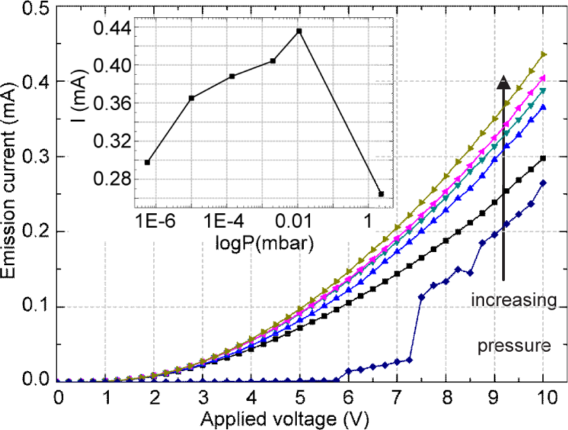
Emission current of the MVG versus the applied bias at vacuum pressures of 2.3 mbar, 1.1×10⁻² mbar, 2×10⁻³ mbar, 1,4×10⁻⁴ mbar, 1×10⁻⁵ mbar and 5.7×10⁻⁷ mbar; the respective inset shows the corresponding I-P characteristics for an applied bias of 10 V
As expected, the FE current increases with the pressure up to about 1.1×10⁻¹ mbar. The I-P characteristic for a potential of 10 V in the inset of Figure 3 shows a nearly linear characteristic in the wide pressure range from 5.7×10⁻⁷ to 1.1×10⁻² mbar. This behaviour was observed to be reproducible and time stable for at least 8 h. For even higher pressures an abrupt decrease in the FE current and unstable operation was observed.
Furthermore the influence of the cathode-anode separation was investigated by comparing the emission properties of the above-mentioned tip (h1=640 nm) and another MVG with a much larger electrode spacing of h2=1.3 μm. As shown in Figure 4a, the increase of the cathode-anode separation results in an increased turn-on voltage of 35 V and a significantly lowered emission current.

(a) Comparison of the I-V characteristic of a MVG with cathode-anode separation of h1∼640 nm (red) and h2 ∼1.3 μm (blue); (b) the respective F-N plots
In order to qualitatively investigate the FE behaviour, the I-V characteristic was plotted according to the FN theory [11], as shown in the respective F-N plot in Figure 4b. The turn-on voltage dependency of the cathode anode separation is best displayed by the increase of the F-N slope with increasing h. The F-N plots are also used to obtain the characteristic field-enhancement factor [12]. For the calculation of the current density of a field-emission device, it is assumed that the electrode surface is planar and the potential within the electrodes constant. For a planar electrode, the electric field is given by E=V/h, where V is the applied voltage and h the distance between the cathode and the anode.
If the cathode has a non-planar structure (i.e., a conical shape), the resulting field non-linearity has to be considered in the calculations. The maximum electric field will be found at the apex of the cathode tip due to the compression of the equipotential surfaces around the cathode. Although the exact calculation of the field-emission current for a sharp cathode requires the numerical calculation of three-dimensional Poisson and Schrödinger equations for electron emission, it is convenient and commonly accepted to introduce a geometry-dependent correction factor given by:

where β is the field-enhancement factor calculated from:

with γ the geometric enhancement factor and h the cathode-diode separation.
Assuming the work function for Au to be Φ=4.8 eV [13, 14] the field-enhancement factor β [15] for our samples was calculated to about 4.2×10⁷ m−1. Even though our geometry deviates from that of the ideal high-aspect-ratio cathode in combination with a flat anode this huge “field-enhancement factor” demonstrates that the nanomachined, cone-shaped cathode and the ring-shaped anode acts as a strong field-enhancement embodiment, enabling a low turn-on voltage of the miniaturized field-emission vacuum gauge.
4. Summary and conclusions
In summary, we have shown an alternative self-aligned fabrication approach for miniaturized cold-cathode vacuum gauges on top of Si-AFM tips. The experiments showed that optimized MVGs operate with very low bias potential and show very good I-P dependence over a remarkably wide pressure range between 5.7×10⁻⁷ and 1.1×10⁻² mbar. By increasing the cathode-anode separation, the turn-on voltage changed accordingly.
The unique geometry of the MVG allows wide-range pressure measurements in systems that require vacuum gauges to operate at low bias potential. The simple structure, compact size and particular embodiment of this MVG also enables spatially resolved pressure measurements, e.g., monitoring the inflow of gases from a nozzle into a vacuum chamber.
Footnotes
5. Acknowledgements
This work was supported by the Austrian Research Promotion Agency (Die Österreichische Forschungsförder-ungsgesellschaft mbH, FFG) and the government of Lower Austria through the COMET programme, as well as the Austrian Society for Micro-and Nanoelectronics (GMe). Furthermore, the authors thank the Centre for Micro-and Nanostructures (ZMNS) for providing the clean-room facilities.