
Abstract
The microphase separation of block copolymer (BCP) thin films can afford a simple and cost-effective means to studying nanopattern surfaces, and especially the fabrication of nanocircuitry. However, because of complex interface effects and other complications, their 3D morphology, which is often critical for application, can be more complex than first thought. Here, we describe how emerging microscopic methods may be used to study complex BCP patterns and reveal their rich detail. These methods include helium ion microscopy (HIM) and high resolution x-section transmission electron microscopy (XTEM), and complement conventional secondary electron and atomic force microscopies (SEM and TEM). These techniques reveal that these structures are quite different to what might be expected. We illustrate the advances in the understanding of BCP thin film morphology in several systems, which result from this characterization. The systems described include symmetric, lamellar forming polystyrene-b-polymethylmethacrylate (PS-b-PMMA), cylinder forming polystyrene-b-polydimethylsiloxane (PS-b-PDMS), as well as lamellar and cylinder forming patterns of polystyrene-b-polyethylene oxide (PS-b-PEO) and polystyrene-b-poly-4-vinylpyridine (PS-b-P4VP). Each of these systems exhibits more complex arrangements than might be first thought. Finding and developing techniques whereby complex morphologies, particularly at very small dimensions, can be determined is critical to the practical use of these materials in many applications. The importance of quantifying these complex morphologies has implications for their use in integrated circuit manufacture, where they are being explored as alternative pattern forming methods to conventional UV lithography.
Keywords
1. Introduction
Block copolymer microphase separation has been demonstrated to form highly arranged patterns of the individual blocks in thin film forms on many substrates [1–4]. Here, the chemical contrast between constituent blocks causes blocks to arrange themselves to maximize favourable intermolecular interactions, but the covalent bond between blocks prevents phase separation on the macroscopic scale. Essentially, the structures formed minimize the surface interfacial area between the different blocks. Using directed self-assembly through either nano-topography or chemical pre-patterning, highly ordered structures can be formed of almost lithographic quality [5]. In this way, BCP thin films have demonstrated considerable promise in microelectronic manufacture and also in other areas where precise nanopatterning of a substrate are required.
Most notably, their thin films' microphase separated structures are being pursued as ‘on-chip’ resist masks for the development of substrate features for device and interconnect/via applications as an alternative to UV lithography (block copolymer lithography [6]). Here, the patterns formed by the microphase separation of the blocks are turned into a topographical mask of one block by selective removal of one or more blocks [7,8]. This produces a topographical polymer pattern that can be used as an etch mask to allow the polymer pattern to be copied to the surface. For use in BCP lithography, the patterns must be very precisely controlled in terms of arrangement, dimension (i.e., domain size, separation) and structural uniformity, and these parameters are controlled by the chemical interactions between the blocks and the composition/molecular weights of the individual blocks [1–4]. The presence of structural defects in the BCP patterns must be almost completely eliminated for application in lithography, with current defect targets of less than 10 over a 300 cm silicon wafer being quoted [9]. It is important that structures are perfectly maintained both across and through the film, as both surface and film bulk morphological defects will be conveyed to the substrate when the pattern is transferred by an etch process[7,8].
Our understanding of the structure/morphology of these films usually comes from microscopy techniques such as atomic force microscopy (AFM) and secondary electron microscopy (SEM), where top-down imaging allows determination of the surface morphology. Alternatively, transmission electron microscopy (TEM) of films removed from the substrate can provide more detailed imaging [10]. Very often, in the study of these systems by these methods, the image contrast between individual blocks is limited, but it can be enhanced if one block can be either removed or selectively stained [11]. As an alternative to direct imaging of the films, if the films are thick enough and the blocks have enough scattering contrast, techniques such as grazing incidence x-ray scattering (GISAXS) can be used to estimate the average domain structure, but these scattering methods usually require synchrotron radiation [12]. These non-imaging techniques are extremely useful, but access to infrastructure can be limited and may lack the required sensitivity to very low defect densities. These approaches will not be discussed here, but clearly have an important role to play in assessing films with large areas.
Consequently, 2D top-down imaging of these films has become the norm as a laboratory-based method of studying the phase separation of these BCP systems, which frequently have feature size dimensions less than 30 nm. However, as feature sizes as low as 5 nm are attained, all of the methods described above can be a challenge, due to resolution problems and contrast (between different blocks) issues, as well as pattern changes through local heating and other forms of beam damage that can occur during length analysis. Furthermore, simple 2D imaging can be limiting as systems can demonstrate complex morphologies [13]. The presence of surface wetting layers can obscure morphology in the interior of the film and require careful etch procedures to reveal the surface 2D pattern formed by the polymers [14,15]. The formation of wetting layers, surface segregation and block-interface affinity, for example, at the surface and substrate interface can precipitate entirely unexpected arrangements in thin films [13]. In addition, as pointed out above, quantifying structural or pattern defects in the surface and through the film is important. For all these reasons, it is important that not only is the surface 2D arrangement quantified, but also the 3D morphology in an effort to fully understand the complexity of the structures. However, proper 3D characterization data has been lacking in studies thus far due to experimental limitations of both the imaging techniques and methods for sample preparation (such as cross-sectioning).
In this work, we describe advances in the experimental techniques that are facilitating proper understanding of BCP systems, and we report results from our laboratories to illustrate progress. We demonstrate that novel techniques such as helium ion microscopy (HIM) offer considerable promise. The inherent resolution limits (0.3 nm) and higher contrast sensitivity for polymer types can afford considerable improvements in image quality compared to conventional electron imaging. Further, the development of highly sensitive SEM apparatus combined with beam energy control might also offer considerable insight into morphology. Finally, the development of methodology to process fastion bombardment (FIB) derived lamellae of soft polymer materials might also allow direct analysis of morphology. This paper reports analysis of a range of symmetric, lamellar forming and cylinder forming diblock copolymer systems.
2. Experimental
2.1 Film preparation
The BCPs used here were either sourced from Polymer Source, Inc. or prepared for us by collaborators [16]. Table 1 details typical block copolymers used here and indicative process conditions. Polymers were dissolved in a suitable solvent and cast onto substrates using spin-coating onto <100> orientated silicon wafers. The substrates had a native oxide layer of ∼2 nm (by transmission electron microscopy). After casting, the films were air dried to remove solvent. The casting solutions were generally between 0.5 and 1 % w/w and were varied to control film thickness. Thickness was measured using ellipsometery. For lamellar forming PS-b-PMMA BCPs, the use of a random copolymer brush was needed prior to film development so that both blocks were favoured at the surface, ordaining the vertical (to the surface plane) orientation of the lamellae. Full details of the application of the brush are detailed elsewhere [17]. All the films described here needed to be annealed for a period of time to develop long range ordering of the microphase separated structures. For PS-b-PMMA a thermal anneal (180 °C under vacuum for 6 h) was the optimum process condition. For the other systems described here, a solvo-thermal anneal was required to reach optimum pattern formation. For PS-b-PEO, the films were solvo-thermally annealed at 50 °C for 1 h in a mixture of toluene and water. PS-b-PDMS samples were solvo-thermally annealed at 40 °C for 6 h and similar conditions were used for the PS-b-P4VP samples. For further details, readers are referred to previous work [17–19].
Characteristics of typical diblock copolymers composed of styrene and methylmethacrylate used for the present study (M.Wt = molecular weight and PDI = polydispersity)

2.2 Characterization
Direct polymer film imaging was carried out on an atomic force microscope (DME 2452 DualScope Scanner DS AFM) operating in AC (tapping) mode under ambient conditions, using silicon microcantilever probe tips with a force constant of 60,000 N m−1 and a scanning force of 0.11 nN. Topographic and phase images were recorded simultaneously. Top-down and cross-sectional images of the films were obtained from a high resolution (< 1 nm) Field Emission Zeiss Ultra Plus Scanning Electron Microscope (SEM) with a Gemini® column operating at an accelerating voltage of 5 kV. Alternatively, an FEG Quanta 6700 SEM was used. An FEI Strata 235-Focused Ion Beam (FIB) tool with resolution up to 10 nm or a Zeiss Auriga dual beam FIB tool (Ga+ Cobra ion column) with an ultimate resolution of 2.5 nm were used to cut lamellae samples for AEM and TEM cross-section analysis. Platinum was e-beam deposited above the patterns followed by the ion-beam platinum deposition. This provided mechanical protection for the weak polymer sections. The TEM lamella specimens were prepared by the Zeiss Auriga-Focused Ion Beam (FIB) with a Cobra ion column of 2.5 nm resolution and were analysed by FEI Titan-Transmission Electron Microscope, operating at an accelerating voltage of 130 kV. Helium ion images were collected on a Zeiss Orion Plus Helium Ion Microscope using an SE2 detector. The samples prepared for the imaging did not have any additional conductive layer cover, and were imaged as prepared or following reactive ion etching, as detailed in the text. The beam energies used for the helium ion microscopy were generally between 20–40 kV with probe currents ranging from 0.1 to 1.5 pA. A 10 μm beam limiting aperture was employed for all the images. Images were formed by collecting the secondary electrons generated during the interaction of the helium ion with the specimen atoms. Charge control was achieved using an electron flood gun. After each line, scan charge neutralization was applied. The image was acquired using either 32 or 64 line averaging.
3. Results
AFM has been traditionally used to examine microphase separation in BCP thin films [20]. This is normally performed in phase mode since there is little topographical contrast. However, as researchers move to BCPs of lower molecular weights in an effort to minimize domain dimensions (feature and pitch size) consistent with state of the art microelectronic device sizes, the resolution of routine AFM instrumentation becomes an increasingly important consideration. Problems are not only based on tip-related issues; contrast changes due to surface roughness can be of the same order of magnitude as those arising from block to block contrast. In Figure 1A, a typical AFM (non-contact phase image) of a phase separated, 45 nm thick PS-b-PMMA thin film is shown. This can quite clearly resolve PS and PMMA domains. However, even at these dimensions (the measured domain spacing is 51 nm with feature size 25.5 nm) the AFM does not produce images where the edges of lines are very well-defined; understanding the domain-domain interface is critical in understanding these systems. In the use of these structures in lithography and pattern transfer, the domains should be separate so that transferred topographies have well-defined and vertical edge shapes [21]. In this way, achieving good quality, high resolution images is critical and SEM might prove to be a preferred option since the nominal resolution is well below these feature sizes. However, image enhancement is normally required. Figure 1B shows a typical SEM image as taken using a conventional field effect electron source. In order to provide topographical contrast, the film has been selectively etched (PMMA removed using an inductively coupled plasma (ICP) dry etch with an argon/oxygen gas mixture as described in detail elsewhere [8]), and, so as to prevent sample charging, a thin layer of gold has been evaporated onto the sample. Whist the image is quite clear, the gold material causes apparent roughening and it has also been noted that the etch can modify and damage the remaining PS structure, which will prevent access to domain interface information.

AFM and SEM images of a lamellar PS-b-PMMA system. A – AFM image of sample. B – SEM image following selective PMMA etch and gold deposition. C –high resolution SEM image of samples and D – high resolution SEM image following partial etch. Images 1 μm × 1 μm.
More advanced SEM instrumentation can be used to reveal the film morphology directly without the use of etching and conductor deposition [22]. Improved secondary electron detection allows some material specificity, thus providing PS and PMMA contrast. Additionally, the possibility of operating at low accelerating voltages limits sample charging and allows micrograph acquisition without deposition of conductor materials. The improvement of the image is obvious (Figure 1C), and the domain separation is sharp, suggesting little domain interpenetration. PS is the material forming the lighter lines in the figure (as proven by selective etching and subsequent cross-sectioning, as described below). It is also obvious, despite what might be expected from the BCP composition, that the PS lines are much thicker than the PMMA lines. We believe that this is because of the lower surface tension of PS (γ = 38 mN m−1; 20 °C) compared to that of PMMA (γ = 41 mN m−1; 20 °C) [23]. As a result, there is some spreading of the PS material at the surface of the lamellar structure and a suggested schematic of this is described in Figure 1C. Evidence for this is seen in Figure 1D, where the same sample following a selective PMMA removal etch shows a more expected structure with the two lines having approximately similar dimensions. In this way, the use of high resolution SEM can provide significant enhanced understanding of these structures, at least for top-down imaging.
Helium ion microscopy (HIM) can provide data of significant value in the analysis of block copolymer patterns data, as described here. HIM can provide resolution between that of SEM and TEM [24] (nominally 0.3 nm is achievable), and this may be critically important as ultra-small domain sizes (as needed for microelectronic device fabrication) will challenge the resolution of SEM to provide useful information on the domain interfaces. HIM also has advantages of improved material contrast (even of similar polymers) and does not suffer from sample charging effects [24,25]. Indicative data for the use of HIM are seen below in Figure 2. Here, images are provided of as-prepared PS-b-P4VP (polystyrene-b-polyvinylypyridine) and PS-b-PEO (polystyrene-b-polyethylene oxide) of small dimension. In Figure 2A, images of ethanol treated PS-b-PEO samples and PS-b-PMMA (of similar domain dimensions around 42 nm) are shown. This ethanol treatment is described further below, but, briefly, provides a means to remove the PEO component and provide topography to enhance image contrast. SEM and HIM microscopy provide clear evidence of the microphase separation of both systems into ordered arrangements. However, the enhanced resolution of the HIM technique is obvious. From these images, the sharp interface between features can be clearly seen and roughness within the line structure can be readily observed and measured. It is also possible to resolve and provide analysis of defects at the surface. E.g., in the SEM area, bright spots can be seen but their origin is not obvious. However, due to the increased depth of field of the HIM technique, it can be seen that these bright spots are raised intersections of the block domains. The depth of field is a critical parameter of any imaging technique, and is particularly important here because surface roughness is a critical consideration since these materials may need to form films of very uniform thickness over large areas.
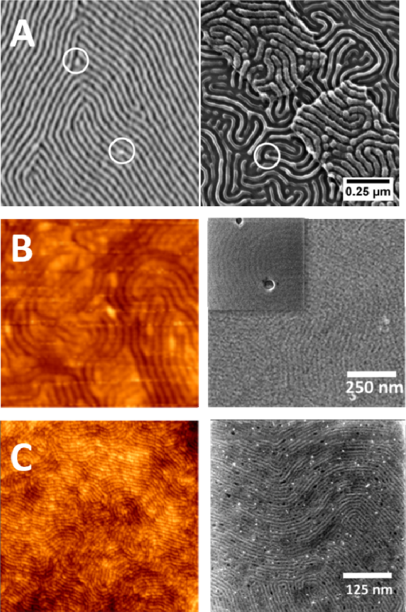
HIM images shown on right and AFM/SEM images on left. A is an SEM image of a cylinder forming PS-b-PEO and HIM image of lamellar PS-b-PMMA system of similar domain spacing (42 nm). Note that typical defect areas are marked. B and C are AFM and HIM images of lamellar forming PS-b-P4VP and PS-b-PEO, respectively. Magnifications for AFM and HIM are identical.
In 2B and 2C, comparisons between AFM and HIM of the same system are described. SEM imaging provided only featureless data because of contrast issues between blocks. Indeed, the PS-b-P4VP system is extremely challenging to image (particularly systems of smaller domain sizes) due to the very similar chemical composition of the blocks. This also makes selective etching using plasma techniques something of a challenge. Figure 2B shows AFM and HIM images of a lamellar forming PS-b-P4VP system of block molecular weights 9.8 × 10³ and 10 × 103 g mol−1 respectively. The domain size is around 16 nm. The AFM image in Figure 2B does reveal indications of phase separation as can be seen in the figure. However, the features seen could be micellar in nature and appear as non-continuous wormhole type features. The domain spacing appears irregular and it is clear that the AFM image represents the limit of resolution. Although it is recognized that this might be improved by tip selection and instrumentation, it is suggested that AFM is not an appropriate methodology for imaging this BCP, as the image shown is a topographical image rather than a phase image which is normally used for imaging BCP patterns. This was because phase imaging produced almost no block identification and we believe that the height variation across the pattern is so small that the image lacks regularity over even quite small dimensions. HIM does allow proper identification of the pattern (the inset of the HIM image is quite clear), as it is a true microphase separated structure with accurate determination of domain size (17 nm), spacing (34 nm) and domain length (0.5 μm), key parameters for quantification. The key observation is that the technique can clearly resolve contrast between two blocks of very similar composition.
Similar data are shown in Figure 2C for a small feature size, lamellar forming PS-b-PEO system (PS-b-PEO, molecular weight 5000-b-5000 g mol−1). AFM (phase image) and HIM images were taken from samples of the same film and substrate. The film has not been treated by etching or other methods to enhance contrast. It is extremely important to examine morphology of these films without additional treatments in an effort to understand these systems. AFM can identify the systems as being phase separated. The size of each domain is around 7–8 nm. The pattern appears to be broken in areas, but the clarity around the nature of the defects, etc., is uncertain. The resolution at the domain interfaces is quite poor. HIM provides a much more informative image and clearly demonstrates the ability of HIM to provide good contrast for the two blocks. Resolution is clearly enhanced and regions where the pattern appears to have missing material are seen as dark areas between domains. The white dot-like structures are due to sample charging and local aggregation of contamination derived carbon moieties.
Returning to the PS-b-PMMA system outlined above, a typical HIM image of the PS-b-PMMA is described in Figure 3. The enhancement of resolution relative to the SEM imaging described above in Figure 1 is obvious. As seen in the SEM data discussed earlier, the PS domains appear thicker than might be expected because of enhancement of PS at the surface. A rich morphology is revealed in an expanded view of a region of this film in Figure 3B. The PMMA domains appear as a darker colour than PS as assigned on the basis of selective etch treatment, as described below. It is clear from the image that there are discontinuities in the PMMA domain structure, with dark spots visible suggesting holes or voids are present within the domains. The formation of voids seems unlikely, because they are not observed (apart from in very discrete locations) in the images shown in Figure 1. We suggest that these darker regions are PMMA, and that in many places PMMA domains have some PS present at their surface. In contrast to the PMMA domains, the PS domains look continuous, which might be expected because of their lower surface energy.

Detailed HIM imaging of PS-b-PMMA. A and B are typical images of unetched BCP thin films. C and D are similar films after a 3 s and 4 s (respectively) etch to selectively remove PMMA. Images A and E are 1 μm2, images B-D are 2 μm2 and F is 0.5 μm2.
To understand this complex morphology further, the sample was progressively etched using the ICP process described above to remove PMMA. It should be noted that this is not a perfect process and the PS is also removed, but at a significantly lower rate than that of the PMMA. After a short etch period (3 s, Figure 3C), the removal of the ‘overfill’ of the PS domain at the surface (Figure 1C insert) can be seen and the domain widths become approximately equal. This image shows that there is still significant PS present in the PMMA domains with clear interconnections between the PS stripes. The PS surface becomes roughened due to the etch process. After an etch of 4 s (about 40 – 50 % of the PMMA removed, Figure 3D), the inhomogeneous nature of the PMMA domains can be readily seen with distinct regions of PMMA and PS resolved and this suggests a complex morphology of the BCP. It should be noted that SEM indicates no topographical variation of the PMMA type domain during an etch variation (Figure 1C is a typical example and taken after an etch period of 4 s similar to the treatment described in Figure 3D), suggesting the description is an appropriate model. Figure 3D and Figure 3E show tilt images (70°) of the sample after a further etch to remove around 70 – 80% of the PMMA. These images show that the complex morphology is not only present in the PMMA domain, but is also in the PS domain with distinct dark regions visible due, it is suggested, to incorporated PMMA.
The images in Figure 3 suggest that a complex morphology of the symmetric BCP exists at both interfaces, and this is described in Figure 4. The top surface consists of a wetting layer largely composed of PS. Above the PS domains, it is somewhat thicker and extends across much of the PMMA structure. Because of surface energy considerations, we propose a ‘mushroom’ shape for the PS lamellae. Below this thin PS layer is the expected lamellar structure, consisting of well-defined stripes of each block. Close to the substrate surface, a mixed phase exists with both PS and PMA present but not in well-defined lamellae. It may consist of poorly arranged regions of each block or it may be a more ordered structure, such as a perforated lamellar structure, but this is not possible to assess. It might be suggested that this unexpected BCP arrangement at the substrate interface could derive directly from the random copolymer (PS-r-PMMA) used as a brush to define surface neutrality. It might also be suggested that the HIM is causing local damage during imaging. However, no evidence for this was seen in the work carried out here. Figure 4B and C illustrate this with typical SEM (Figure 4B) and HIM (Figure 4C) images of an unetched PS-b-PMMA self-assembled film. The electron beam damage needed to obtain high resolution images can be clearly seen in the figure as a pale square, probably due to e-beam reduction/degradation of the polymer in order to yield carbon. The HIM image in Figure 4C shows no sign of damage. This is due to the lower beam current and shorter collection times needed to obtain equivalent or better resolution images.

A – a schematic of the proposed structure of the PS-b-PMMA lamellar film. B and C are SEM images showing the possibility of damage under electron beam analysis. Images are 1
Transmission electron microscopy (TEM) can also provide significant detail of BCP films, although, as discussed earlier, this technique is particularly challenging because of the ‘soft’ nature of the materials, particularly when examining thin films on substrates [26–29]. This makes sample preparation difficult and the technique is further complicated because the contrast between the blocks is usually similar. Despite these issues, TEM is becoming an ever more important metrology in this area for two main reasons. Firstly, and as discussed above, many researchers are moving towards very small domain sizes where techniques such as SEM and AFM have limited resolution and where the use of techniques such as HIM are, as yet, uncommon. Secondly, if block copolymer lithography is to be realized for the manufacture of small transistor devices, it is absolutely critical that morphology through the film to the substrate surface is known so that effective pattern transfer to the substrate can occur. For these reasons, various practical techniques have been used to allow the use of TEM. Commonly, removing the film by solvation of a substrate (e.g., salt) and mounting on to a sample holder has been used to provide high quality, high resolution BCP thin film imaging and allow more complete understanding of these systems [30]. Of course, the use of ‘model’ substrates ensures that questions about film structure on the most relevant substrates such as silicon still remain.
TEM can have a very high impact in these studies because of its ability to image the 3D morphology of BCP films if thin cross-section samples can be produced. However, cross-sectional TEM studies of BCP films produced by focused ion beam (FIB) (and similar methods) are rare [31], with the first analysis produced in 2001 [32]. As has been stated earlier, the lack of image contrast of different blocks, the normal difficulties in generating TEM lamellae of soft materials and the availability/cost of the instrumentation required have prevented widespread use of the methodology. TEM contrast can be enhanced by selected inclusion of inorganic materials (the use of heavy metal ions, commonly known as staining), or by the selective removal of one of the blocks [33]. These staining/removal methods can also be combined with XTEM to provide side views of the BCP morphology whilst still attached to the substrate. A typical example is shown in Figure 5 for the cylinder forming PS-b-PEO structure. Here, AFM (Figure 5A) and SEM (Figure 5B) can be used to resolve the top-down film structure. Note that the SEM image has been generated by exposure of the film to ethanol (ultrasonic treatment at room temperature for around 12 h) to remove the majority of PEO block. All of the images reveal that hexagonal cylinder structure with cylinders orientated perpendicular to the crystal plane. However, XTEM reveals a more complex structure of this ethanol treated film (Figure 5C). It is instantly apparent that the ethanol is effective in removing the PEO to produce a corrugated structure as might be expected. However, the image also suggests that the cylindrical morphology does not extend through the substrate surface and a well-defined PS wetting layer (around 8 nm thick) is present at the substrate-BCP interface. The wetting layer thickness is somewhat less than might be estimated using <h2>0 = Mw* 0.43 (<h2>0 is the mean-square end-to-end distance of the polymer coil and Mw is the molecular weight [34]). This estimates the coil size at about 11.6 nm which is somewhat bigger than observed here, but some in-plane strain might be expected, causing compression of the thin PS wetting layer.
AFM (A), SEM (B) and TEM (C) images of PS-b-PEO. See text for details. In the TEM image, Pt is an e-beam layer deposited during cross-section FIB preparation to protect the mechanical weak polymer layer.
In this way, imaging films that exhibit a hexagonal cylinder morphology and a vertical orientation (similar to the lamellar structure) can be readily achieved. However, the inclusion of contrast agents (normally heavy metal ions) or block etching may cause changes or alteration in morphology.
Furthermore, while inclusion of contrast agents post-film preparation by selective techniques such as CVD and chemical affinity might be possible when blocks are exposed at the surface, it is less clear how parallel orientated cylinder morphologies might be accessed. Similarly, selective etching is problematic because the cylinders are usually buried below the surface and ‘tuning’ etches to precise depths, exposing a sub-surface structure and then removing a second material requires very significant effort. Of course, direct imaging of the structure would be favourable but, as has already been stated, lack of TEM contrast to different polymer blocks provides very significant challenges in addition to the normal problems associated with cross-sectioning soft materials. However, modern microscopes and refinement of lamellae preparation that has been developed to allow imaging of biological materials can, in favourable circumstances, allow direct imaging of BCP nanopatterns, although this work is in its infancy and requires improvement in order to be described as routine.
Figure 6 shows SEM, AFM and cross-sectional TEM from another cylinder forming PS-b-PEO film, which has been processed to give a parallel cylinder orientation (to the surface plane). SEM (i.e., etched as described for data presented in Figure 6) and AFM (unetched) images of ethanol treated samples clearly show the top-down patterns. The cylinders have well-ordered arrangements and are regularly spaced and parallel over micron areas. Cross-section TEM indicates a more complex arrangement. Typical data are shown in Figure 6C, with a schematic version of the same data in Figure 6D. The TEM reveals the presence of two layers of cylinders (as expected from the film's thickness), but it is clear that the two layers of cylinders are markedly different. The upper surface shows the effect of this extended ethanol exposure. Clearly, PEO cylinders that were present at the upper surface of the film have been removed resulting in surface corrugation of the polystyrene component. A part-schematic in Figure 6D shows a proposed structure of the original film. The upper cylinder layer appears to have had spherical-like cross-sectioned cylinders as the height of the PS corrugation agrees with the cylinder diameter of ∼ 17 nm as measured by SEM and AFM. EM micrograph is the surface profile (dashed line) recorded in Figure 5. Also, as the cylinder-to-cylinder spacing measured at this upper surface layer by TEM is (within experimental error) close to that measured in the top-down images at 32.8 nm. As well as the surface features, ‘cylinders’ closer to the substrate surface unaffected by the ethanol etch treatment can just be resolved. Note that ethanol is not soluble in and does not swell PS, and the sub-surface PEO features are unaffected by treatment. The difference of contrast between these and the background polystyrene is not dramatic, but their presence is obvious. They are reasonably reproducibly spaced and sized. However, the elliptical nature of the cylinders is very obvious, as is significant compression from an ideal circular cross-section. We suggest the cylinders are compressed by the film strain present. In-plane film strain is expected for all thin films, although additional strain might result from solvent evaporation during film formation and processing. It should also be noted that the spacing of the sub-surface PEO cylinders is not the same as the surface features and can be measured at about 28.0 nm. The reason for this contraction is unknown at present. Further, the structure of the cylinders as represented in Figure 6 is not a simple hexagonal arrangement. If this were the case, the spacings between the cylinders should be similar at the surface and sub-surface, and this is clearly not the case, as noted above. It would also be expected that the cylinders would lie directly below the polystyrene corrugation, and this is also not seen in this or any other images collected. This is an important observation and reiterates the point made above that the bulk morphology cannot be readily predicted by simple top-down images. In this example, it may be argued that the formation of a polystyrene wetting layer at the polymer-substrate interface reduces the amount of polystyrene in the region of the sub-surface layer of cylinders; the PEO cylinders, therefore, pack a little more closely together.

AFM (A), SEM (B) and TEM (C) images of a PS-b-PEO film on a silicon substrate. See text for further details. D is a part-schematic of C showing positions and shapes of PEO cylinders.
In both Figure 5 and Figure 6, the rounded shape of the corrugated polystyrene at the surface that results from the ethanol etch is obvious. The reason for this rounding is not clear. It may arise from a number of factors. One possible cause is that the cylinders are wider at the surface. This seems unlikely because the width of the cylinders in both vertical and horizontal orientations is about 14.4 – 14.6 nm (measured from the non-etched AFM images and averaged over 50 individual domains) and this is consistent with the volume fraction. It is also only slightly less than the average width of the buried cylinders in Figure 6C, which was around 14.7 nm. Instead, we suggest that the rounded shape derives from deformation of the nanostructured polystyrene pattern, i.e., the polymer is not rigid enough to support itself.
Because the system is wholly organic in nature, direct imaging of the PS-b-PEO system is a considerable challenge. Inorganic inclusion, staining and selected block removal can help resolve some of the problems, but an example of how these techniques can subtly and less subtly alter the pattern is provided above. Some pattern forming BCP systems contain inorganic atoms such as silicon as part of the block structure. A common example is PS-b-PDMS, which is considered a highly promising system because of its ability to form very small features and act as a good etch mask for pattern transfer [13–15]. This system is described further below.
Control of the PS-b-PDMS system is difficult. The PDMS block is highly hydrophobic and achieving films of regular thickness across large areas is challenging. The use of molecular brushes or surface functionalization is almost always necessary to provide a suitably similar hydrophobic surface [35]. Further, the low surface energy of PDMS compared to PS and the hydrophobic nature of the substrate surface can lead to PDMS wetting layers at both the substrate and air interfaces [35]. For these reasons, lamellar systems usually arrange with lamellae parallel to the surface plane and are consequently of little effective use in forming the more practical stripe patterns seen above for the lamellar forming PS-b-PMMA system. For these reasons, the cylinder forming compositions have been extensively fabricated as a means to form both vertical cylinder structures and stripe patterns depending on the cylinder orientation. Imaging of these is problematic because of the surface PDMS wetting layers and, initially, the top-down AFM and SEM images are featureless. Various etch procedures have been developed to remove these layers and expose the patterns for study.
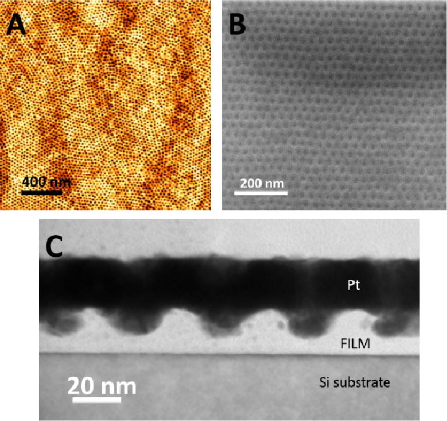
High resolution SEM can be used to image PS-b-PDMS structures following a plasma pre-etch to remove the upper layer of PDMS [13–15]. A typical example can be seen in Figure 7. The low resolution image appears to show light and dark regions of sizes 10–50 μm. These might be explained by an island-hole structure with the polymer not coating the entire surface. However, higher resolution images of an area around one of the light-dark interfaces (Figure 7B) show that not only does the polymer cover the surface, the microphase separated pattern extends through the region. The area of the colour change is indicated by the white dashed line and the region at the bottom of the image is noticeably darker grey. Detailed TEM cross-section images (see below) show that the contrast is due to the thickness of the film. In the darker regions, the film is thicker with two layers of cylinders, whilst the lighter regions of the film are only one cylinder thick. The ability of SEM to ‘image’ thickness variations in this way is important. It not only allows proper film quantification, it also allows the thickness to be very carefully optimized to allow formation of exact cylinder monolayer thicknesses in a relatively easy manner. Techniques such as ellipsometery yield only average values while cross-section analysis is more time consuming and, obviously, destructive. It is necessary for some applications to generate single layer cylinder structures. For example, if the BCP pattern is to be transferred to the surface via techniques such as material selective plasma etching, multilayers are not suitable because there is little variation in material composition through the film.

SEM images of a cylinder forming PS-b-PDMS film on a silicon substrate at (A) low and (B) high resolution. Inset shows a schematic of the arrangement in the light and dark regions clearly visible in A and B
As suggested above, the bulk morphology of these films can be complex because of the possibility of wetting layer formation. For this reason, high resolution TEM cross-sections as described above (Figure 8) were studied to reveal these morphologies. The presence of these wetting layers have previously been inferred by spectroscopic methods but have not been directly revealed previously. They can easily be resolved using these imaging methods. Figure 8A shows a TEM cross-section of the PS-b-PDMS film deposited onto a PDMS brush layer (a hydroxyl terminated PDMS homopolymer used to allow full coverage of the surface as described above). Note that the sample was not pre-etched to remove any wetting layer. Film thickness was very carefully controlled to give a uniform monolayer of cylinders across the surface. Wetting layers of PDMS at the surface and the substrate interface can be seen but the substrate-polymer wetting layer is somewhat thicker because it is made up of the brush and the BCP component.

Cross-section TEM images of cylinder forming PS-b-PDMS on planar (A and B) and topographically patterned silicon substrates (C)
The well-arranged PDMS cylinders can also be seen and clearly have an elliptical shape which is ascribed as being due to in-plane stress developed during processing, as described earlier. This distortion is regularly seen by us in many systems and is particularly noteworthy for systems that have been processed using solvent annealing. This may be related to the strain imposed during solvent evaporation.
In Figure 8B, another region of the same film is shown, and this reveals the real advantages of using these methods of studying the 3D morphology rather than just the top-down structure. A large defect can be seen at the substrate-polymer interface. Viewed from the top, the pattern may well look non-defective, but here the missing cylinder is quite obvious. The origin of this defect is unknown, but one possible explanation may be the presence of a homopolymer defect in either the brush or BCP. Because of its size, it is unlikely to be due to a BCP with a very large PDMS block.
The advantage of this cross-sectioning technique is that the samples do not have to be pre-etched to reveal the underlying structure. This is clear since the exterior PDMS wetting layer is clearly visible. A cross-section image of a film that has been pre-etched is shown in Figure 8C. It is obvious here that this ‘stripping’ of the wetting layer results in not only its removal but also the removal of some PS, so that a layer of isolated PDMS cylinders can be seen at the outermost surface. These have probably been oxidized during the plasma etch process. This film is substantially thicker and contains four rows of cylinders, all distorted due to the strain described above. The substrate wetting layer can also be clearly seen. This film was created in a topographically patterned substrate consisting of parallel channels lithographically cut into the substrate. These structures are commonly used to ordain the directed self-assembly (DSA) of the patterns separated by microphase [36]. Here, the sidewalls are preferentially wetted by one block, causing the cylinders to align with the sidewall direction, a technique known as graphoepitaxy [36]. DSA is of considerable interest if the patterns are to be used for the creation of nanoelectronic devices [37,38]. This thicker film clearly shows the hexagonal type arrangement of the PDMS cylinders. However, it can be seen that not only are the individual cylinders distorted by the film strain, but so is the hexagonal type arrangement with the unit cell being highly compressed, so that the lattice parameters in the <0,1> and <0,1> directions (as defined in the figure) have a ratio of about 1.8 rather than the expected value of 1 for an ideal hexagonal arrangement. The hexagonal arrangement is also distorted at the sidewalls, suffering both rotational and spacing distortions. This additional distortion arises from two factors. The first is the shape of the lithographically patterned sidewalls. The second is the way that the polymer fills the channel during coating with obvious surface tension effects present and manifest in a bowed surface.
This type of imaging can provide clear insight into the surface chemistry. As described above, the ‘chemical engineering’ of the substrate surface is almost a prerequisite for controlling the surface coverage, thickness uniformity and orientation of the polymer pattern. Figure 9 illustrates the capability of cross-sectioning and surface engineering for PS-b-PDMS films so that films with different polymer-surface interfaces can be seen. Here, we can readily see interfacial layers of PS (Figure 9A – a surface that has been functionalized with a brush, a hydroxyl terminated PS homopolymer (PS-OH)), PDMS (Figure 9B, a PDMS-OH functionalized substrate surface) and half-cylinders of PDMS (Figure 9C, substrate without any functionalization) can be readily observed. Note that the hydroxyl termination allows the brush to be firmly attached to the surface via condensation reactions with surface silanol moieties. The arrangement seen in Figure 8 and 9C is shown for a PDMS brush and is described in the schematic. The PDMS brush has obviously favourable interactions with the PDMS block and results in a well-defined PDMS wetting layer. Use of a PS-OH brush instead of the PDMS-OH results in a PS wetting layer, as might be expected. The silicon substrate and its passive silica layer is surprisingly neutral in terms of its interactions with the polymer blocks, and allows both PDMS and PS to reside at the substrate surface. The result is a regular arrangement of PDMS half-cylinders at positions defined by a pseudo-hexagonal arrangement. Whilst these studies clearly add to understanding of these systems, they are also important for applications since the presence of wetting layers is a challenge if the patterns are to be successfully transferred to the substrate.

Various (A – C) images of PS-b-PDMS on substrates of different surface chemical functionality. A schematic (D) describes the arrangement shown in C. See text for details. Scale bar is 40 nm in all cases.
4. Closing Remarks
The morphological complications that exist in BCP films are of clear scientific interest in terms of understanding block-block interactions and the structure that forms because of these. Of particular importance is how the polymer blocks interact with interfaces, modifying the structure observed. It must be emphasized that complex 3D morphologies will have strong implications in the application of these materials in emerging technological areas. Block copolymer lithography for use in development of nanoelectronic circuitry, as introduced very briefly above, is seen as one such application. Here, the pattern formed by the microphase separation of the polymer blocks into nanodomains is used as a template for creation of substrate features (pattern transfer). Various methodologies such as templating and selected material deposition are possible. In the most industry compatible technique, one block is selectively removed (by gas or liquid phase etching) to expose areas of the substrate, while non-exposed areas are covered by an etch-resistant on-chip mask which allows a second etching process to pattern transfer the patterned polymer structure to the surface. This can be applied for the creation of both line (for fabrication of interconnect and nanowire device structures) and hole (for via structures) patterns. The need for the BCP pattern to have precise and reproducible regularity both across the substrate and through the depth of the film is obvious. While great progress in defining patterns of low surface defectivity has been made and development of controlled etch processes demonstrated, a proper assessment of 3D morphological effects and how they might affect the quality of transferred features has not yet been performed. The considerable challenges in defining highly regular structures through the film are illustrated below with the specific example of a cylindrical PS-b-PDMS system.
In Figure 10, a schematic showing an idealized scheme for enabling the pattern transfer of a complex PS-b-PDMS hexagonal pattern to a substrate is described [13–15]. The original form of the BCP layer as described above is shown in Figure 10A. Briefly, the surface wetting layer must be removed to expose the spatially arranged PDMS cylinders (Figure 10B). This will also result in some PS removal, but is unlikely to remove all of the exposed polymer. The remaining exposed PS must then be removed to produce a topographical resist mask of PDMS/PS features (Figure 10C). Oxidation of the PDMS is then needed to produce an etch-resistant ‘hard-mask’ (Figure 10D). However, the PDMS derived silica type moieties now sit in a silica-like PDMS derived wetting layer. Exposure to a non-selective topographical etch is then required to expose silicon for the final pattern transfer (Figure 10E). A silicon-specific etch can then be used to pattern transfer into the substrate as shown in Figure 10F. Finally, the oxidized PDMS, the PS and the PDMS layer must then be removed using a non-specific etch (Figure 10G). As can be seen in Figure 10, 3D morphological issues such as multilayer formation, orientational non-uniformity and shape problems can result in pattern transfer problems.

Idealized steps in the pattern transfer of a complex BCP film to a substrate. See text for further details
Therefore, it is suggested that much more work is required in the study of these systems. The work needed is both time- and cost-consuming. Producing samples for XTEM is difficult and prone to failure. Techniques such as HIM are in their infancy and access to equipment limited. Of course, preparing high quality films requires many laboratory hours perfecting coating and processing techniques. It is obvious that many laboratories will be limited by access to dedicated dry etch facilities. The techniques require further development. Are other techniques capable of detecting minority structural defects available? It is clear that these advanced forms of microscopy are ‘destructive’ and could not, for example, be used to monitor in-line processes. Challenges exist. Could SEM imaging and analysis be improved to allow rapid, large area analysis? Could the techniques be developed, by, e.g., tilt-imaging, to provide simple analysis of 3D structural defects? Quantitative, automated and software controlled defect detection and analysis is all-important, and only limited attempts have been made to date to provide user-friendly software. The biggest challenge is for these metrologies to keep pace with ever decreasing feature sizes where near-atomic resolution will be required to image feature roughness and defectivity.
The aim of this article has been to highlight these issues and familiarize readers with the state-of-the-art. Hopefully, it will support the developments required to bring block copolymer assembly to both scientific and technological maturity.
Footnotes
5. Acknowledgements
The authors thank SFI (Research Centre Grant AMBER, SFI 12/RC/2278 and Principal Investigator Grant 09/IN.1/I2602) and the EU ENIAC support for PLACYD.