
Abstract
This paper presents the design of a graphene-based electronically tuneable microstrip attenuator operating at a frequency of 5 GHz. The use of graphene as a variable resistor is discussed and the modelling of its electromagnetic properties at microwave frequencies is fully addressed. The design of the graphene-based attenuator is described. The structure integrates a patch of graphene, whose characteristics can range from being a fairly good conductor to a highly lossy material, depending on the applied voltage. By applying the proper voltage through two high-impedance bias lines, the surface resistivity of graphene can be modified, thereby changing the insertion loss of the microstrip attenuator.
1. Introduction
During the past number of years, scientific interest in graphene has experienced impressive growth due to the extraordinary mechanical, electronic and optical properties of this material [1]. Graphene is a one-atom-thick two-dimensional carbon crystal retrieved in many materials such as highly ordered pyrolytic graphite (HOPG), which consists of many graphene sheets stacked together in a pile. Due to its outstanding properties, such as a carrier mobility attaining 200 000 cm2/Vs at room temperature, the question has been posed whether graphene may be exploited for microwave applications in the GHz range. As a matter of fact, the unique properties of graphene are being exploited in radio-frequency nanoelectronics [2] to realize novel high-speed devices such as field effect transistors [3], frequency multipliers [4] transparent solar cells [5], meta-materials [6] and graphene plasmonics [7]. Nevertheless, the possibility of using graphene in passively guided devices and antennas from microwaves to THz has been less explored. This is mainly because such structures require electric sizes in the order of the wavelength, while the size of the first available graphene samples was much smaller. However, graphene chemical vapour deposition (CVD) currently allows for obtaining samples of up to several centimetres, which has increased the research interest for realizing passive devices at such frequencies [8].
In this paper, we discuss the use of graphene as a tuneable resistor at microwave frequency. In particular, we present the preliminary design of a graphene-based electronically tuneable microstrip attenuator operating at a frequency of 5 GHz. This concept lays the groundwork for the development of tuneable microwave and mm-wave passive components, either in microstrip line [9] technology or in substrate integrated waveguide [10] technology, which is likely to represent the fundamental building blocks for the realization of future transmitting/receiving (T/R) nanoscale microwave communication systems. We have performed the design and modelling of the microstrip attenuator; currently, we are dealing with the fabrication of the device, with a graphene patch being sourced from a CVD sample.
2. Graphene properties in the microwave range
In the micro-/mm-wave range, by considering graphene samples of the order of mm2 or cm2, we have moved beyond the ballistic regime (the mean-free path for ballistic carrier transport is 500–1000 nm at room temperature) and as a result, a drop in graphene carrier mobility has occurred.
Nevertheless, two main breakthroughs and strictly related properties remain valid: i) ambipolarity and ii) tuneability.
By applying energy to the graphene, we can shift its Fermi level and modify/control its electrical properties; when the Fermi level moves into the valence or conduction band, the hole or electron conduction begins to dominate the current transport and as a result, the resistance becomes low. This energy can be provided by an external electrical field (potential).
The gate-induced carriers can be seen as resulting from electrical doping, analogous to the chemical doping typically used for semiconductor devices [11]. The difference is that semiconductor doping is an irreversible process, while graphene electrical doping is completely reversible.
In graphene, the electrons and holes are electrically induced by applying a positive or a negative voltage with respect to a reference electrode (e.g., ground, gate etc.). Moreover, it has also recently been demonstrated that graphene can be efficiently used as passive substrate with variable resistance, permitting microwave devices to be tuned in order to obtain the proper matching [11].
The combination of i), ii) and the possibility of having samples of up to several centimetres (by CVD fabrication) has made it possible to enable a new class of reconfigurable microwave devices (e.g., attenuators, phase shifters, patch antennas, etc.) with unprecedented performance in terms of mass, volume and power consumption when compared to current implementations, as well as completely new microwave applications currently not available, such as slow-wave structures (e.g., leaky-wave broadside antennas) [12] and graphene patch antennas [13].
Concerning the electromagnetic-quantum transport characterization, since graphene is a mono-atomic layer, [14]. This tensor depends on graphene's unique band structure and on a number of parameters including temperature, scattering rate, Fermi energy, electron velocity, pre-doping (not all these parameters are independent), as well as electrical and magnetic field bias. In practice, other parameters such as defects in the potential polycrystalline nature of the graphene can further affect its properties. In general, the conductivity of graphene is particularly frequency-dependent and can have completely different behaviour at, for example, microwave and THz.
3. Graphene modelling in the microwave range
The 2D tensor of graphene in cylindrical coordinates comprises diagonal (σ ∥) and off-diagonal (σ⊥) conductivities, which are usually derived using the Kubo formula. The latter can be reduced to a simple Drude model if the condition uc»ħω, where uc is the Fermi level of graphene and ω is the frequency, [14] holds:
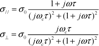
where

All is the DC limit of graphene conductivity, with scattering time τ, temperature T, Boltzmann constant k

Real and imaginary parts of the surface conductivity of graphene at room temperature and in the absence of a magnetic field, as a function of uc from DC up to hundreds of GHz
It is noted that, based on (1), with typical values for the involved parameters, the graphene conductivity is almost constant [1] from DC up to hundreds of GHz.
In the current design, the adopted graphene patch was obtained by applying the CVD technique. It has the following nominal characteristics: transparency >97%; number of graphene layers: 1; thickness (theoretical): 0.345 nm; FET mobility on Al2O3 2,800 cm2/V·s; Hall mobility on SiO2 3,500 cm2/V·s; sheet resistance 170 Ohm; grain size of up to 10 µm. The graphene sample is also equipped with an appropriate kit for its transfer onto the device.
4. Design of the tuneable microstrip attenuator
The applicability of graphene for the implementation of tuneable microwave components is demonstrated in this section by the preliminary design of a voltage-controlled microstrip attenuator, operating at a frequency of 5 GHz.
The circuit consists of a graphene patch connected to input and output microstrip lines (Figure 2). In order to bias the graphene with the proper voltage, two high-impedance bias lines are used at the opposite sides of the graphene patch. In addition, radial stubs are adopted as low-pass filters, to prevent the propagation of the RF signal along the bias lines (Figure 2b). Moreover, to separate the microstrip ports of the circuit from the DC bias, interdigital capacitors are inserted in the input and output microstrip lines (Figure 2c). Finally, to match the different widths of the graphene patch and of the 50-Ω microstrip lines, two microstrip tapers are adopted (Figure 2d).

Layout of the voltage-controlled microstrip attenuator, operating at 5 GHz (dimensions in mm: L=47.4, LT=16.715, Wm=1.1, g =0.25, WT=0.445, α=90°, W1 =0.4, L1=9.575, r=6.5, Ltaper=3): (a) complete circuit; (b) high-impedance bias lines with radial stubs; (c) interdigital capacitors; (d) microstrip tapers used to match the different widths of the graphene patch and of the 50-Ω microstrip lines
The circuit was designed on Taconic RF-35 dielectric substrate with a thickness of t=0.5 mm, a relative dielectric permittivity of εr=3.5 and a loss angle of tanδ=0.0018. The conductivity of the copper metallization is assumed to be σ=5.8107 S/m and the metal layers are considered infinitely thin. The width of the 50-Ω microstrip lines is 1.1 mm.
A microstrip circuit without graphene was preliminarily designed, where the graphene patch was replaced with a square copper patch. This circuit represents the structure that embeds the graphene patch in the tuneable attenuator and it is applied with a de-embedding purpose. The metal patch is a square with the dimensions LG=WG=1.1 mm, i.e., with the side equal to the width of the microstrip line. In this way, a continuous straight microstrip line is obtained. By using Ansys HFSS, the circuit was optimized for minimum insertion loss at 5 GHz. The dimensions of the circuit are reported in Figure 2. The simulated frequency response of the circuit in terms of scattering parameters is reported in Figure 3 (dark grey lines). The insertion loss of the circuit, calculated between port 1 and port 2, is 1.51 dB at a frequency of 5 GHz.
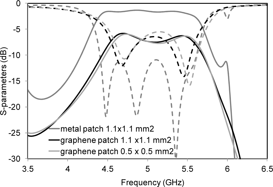
Full-wave simulations of the voltage-controlled microstrip attenuator: scattering parameters versus frequency are shown in the cases of a metal patch and with graphene patches of different sizes and a surface resistivity of 80 Ω (|S11|: dashed lines, |S21|: solid lines)
Subsequently, a circuit with the same geometrical dimensions was considered where a graphene patch was inserted into a gap of the microstrip line (Figure 2). The size of the graphene patch was LG=WG=1.1 mm, so that no tapers were needed in the microstrip lines. Full-wave simulations were performed by modelling the graphene as a patch with surface resistivity of 80 Ω and the results are shown in Figure 3 (black lines). The resistivity of the graphene, which was higher than the resistivity of copper, determined a larger i.e., the calculated insertion loss between port 1 and port 2 was 7.35 dB at 5 GHz. This loss was partially attributed to two major effects: the first was the loss of the embedding circuit, as previously calculated for the circuit without graphene, while the second was the loss due to the graphene patch, which can be partly attributed to ohmic dissipation and partly to reflection.
By changing the value of the bias voltage applied to the graphene patch through the high impedance bias lines, the surface conductivity of graphene can be modified according to the plot shown in Figure 1. Consequently, the insertion loss of the microstrip attenuator can be electronically tuned.
The loss as a result of the graphene patch is calculated by analysing the structure in Figure 2d, after de-embedding the insertion loss of the microstrip lines. The resulting insertion loss of the graphene is shown in Figure 4 (black line) versus the value of the graphene surface resistivity. A tuning range from approximately 1.7 dB to 13 dB can theoretically be achieved.

Insertion loss due to the graphene patch vs. surface resistivity for two dimensions of the graphene patch. The insertion loss is calculated at 5 GHz after de-embedding the effect of the microwave circuitry.
The shape and size of the graphene patch affect the insertion loss of the attenuator. In particular, when increasing the length of the graphene patch, the insertion loss increases. Figure 5a shows the insertion loss due to the graphene patch (after de-embedding the microstrip circuit) calculated at 5 GHz, versus the length LG of the graphene patch (Figure 2d) while keeping the patch width at the nominal value WG=1.1 mm and maintaining graphene surface resistivity of 80 Ω. The insertion loss grows almost linearly alongside patch length.

Insertion loss due to the graphene patch for different shapes and sizes of the graphene patch. The insertion loss is calculated at 5 GHz with a graphene resistivity of 80 Ω, after de-embedding the effect of the microwave circuitry. (a) Insertion loss vs. length LG (with WG=1.1 mm); (b) insertion loss vs. width WG (with LG=1.1 mm); (c) insertion loss vs. square side LG=WG.
When modifying the width of the graphene patch, tapers are needed to connect the patch to the microstrip lines with minimum discontinuity (Figure 2d). Figure 5b shows the insertion loss as a result of the graphene patch (after de-embedding the microstrip circuit) calculated at 5 GHz versus the width WG of the graphene patch (Figure 2d), while keeping the length at the nominal value LG=1.1 mm. The insertion loss is large when the width of the graphene patch is small, because this case corresponds to a large current density flowing through the graphene; the loss decreases when increasing the patch width.
When the shape of the graphene patch is square (LG=WG) and the size is modified, the two effects discussed above tend to compensate. Figure 5c shows the insertion loss due to the graphene patch (after de-embedding the microstrip circuit) calculated at 5 GHz, versus the side LG=WG of the graphene patch. The simulation shows that the insertion loss does not practically change for the different values of the patch size: for instance, the same insertion loss can be achieved by using a graphene square patch with a size of 1.1×1.1 mm2 or 0.5×0.5 mm2.
In order to confirm this result against frequency, the circuit was analysed by considering a graphene patch with a size of LG=WG=0.5 mm and the results are shown in Figure 3 (light grey lines): the frequency response of this circuit is almost identical to the response of the circuit with a larger graphene patch (with size LG=WG=1.1 mm).
Similarly, the insertion loss due to the graphene patch vs. surface resistivity was calculated in the case of a graphene patch with a size of LG=WG=0.5 mm and the results are reported in Figure 4 (light grey line). No substantial differences were observed between the two cases with square graphene patches of different sizes.
5. Conclusions
The use of graphene as a variable resistor was discussed in this paper with the aim of implementing of an electronically tuneable microstrip attenuator. Depending on the applied voltage (which in turn modifies the surface resistivity of graphene), the proposed attenuator exhibits a tuneable insertion loss ranging from 1.7 to 13 dB. The impact of the size of the graphene patch on the attenuation of the circuit was widely discussed. The miniaturization of the graphene patch was also considered.
The concept discussed in this specific case can be easily extended to several different classes of passive microwave and mm-wave components in microstrip, coplanar and substrate integrated waveguide technology.
Footnotes
6. Acknowledgements
This work has been supported by the European Project, “Carbon Based Smart Systems for Wireless Applications”, (NANO-RF, n. 318352).