
Abstract
The influence of sol-gel dip-coating and anodic oxidation process parameters in producing thin TiO2 films is studied. As the size of the films is in the order of nanometres (20–140 nm), to obtain a precise measurement of their thickness and analyse their crystalline structures, glancing incidence angle X-ray techniques (X-ray reflectometry and X-ray diffraction) using synchrotron radiation are used. A relationship between the colour and thickness of the films was found. This enables the film thickness to be estimated by the film colour. Within the range of the parameters studied, both techniques produce thin films with smooth surfaces which at most reproduce the roughness of the polished substrate. Independently of the technique, thermally-treated films thicker than 30 nm presented different crystalline structures with anatase and rutile phases.
1. Introduction
At present, titanium alloys are used in prosthetic devices for human implants due to their excellent biocompatibility [1]. The biological and chemical properties of titanium alloys are known to be associated with the natural formation of TiO2 on their surface. The thickness of the naturally formed oxide is between 2 nm and 10 nm. This native oxide film often has a high density of defects (mainly cracks), which give poor mechanical properties such as low resistance to wear [1,2]. In addition, the dissolution of the underlying metal after the rupture of the oxide film and the subsequent reformation of the passive oxide layer result in the gradual consumption of the material [1]. Thus, a combined wear and corrosion process occurs [3]. In general, coatings on metals are widely used to incorporate (or improve) the tribological, biological, corrosion, or aesthetic properties of a component. In this way, according to previous reports, artificially TiO2-coated Ti alloys are more resistant to dilution in simulated body fluids than non-coated ones [4,5]. Also, the growth of thicker films could improve mechanical resistance by increasing the amount of material available to hold the loads and resist the wear while the components are in use. Thermal oxidation, anodic oxidation and the sol-gel process are simple and inexpensive techniques in which the oxide is artificially formed by exposure to high temperatures, electrical current or some chemical reagent, respectively [6,7]. These methods are also advantageous because they coat the substrate in an omni-directional way.
To build a new prosthetic heart valve (as described in a previous work [8]) a Ti-6Al-4V alloy coated with TiO2 was preferred [5], since this application requires a haemocompatible surface. According to the literature, the morphology of the surface, roughness and crystal structure of the coating all have an influence on its haemocompatibility [9]. The thickness and homogeneity of coatings (without cracks) are important in the corrosion response of the material in avoiding ion release. Cigada et al. [10] have shown that corrosion resistance in simulated body fluids increases considerably with anodic TiO2 films thicker than 20 nm. Velten et al. [5] have reported that the corrosion resistance of Ti alloys in samples with a TiO2 layer is increased independently of the oxidation procedure.
Nanoscale surface roughness is also essential for haemocompatibility because rougher surfaces expose a larger area to the bloodstream, which can easily result in blood coagulation. However, for a blood-contacting implant, a rougher surface will result in a decrease in the clotting time and an increase in the number of adhered platelets [9,11]. In contrast, in the case of hard tissue implants, a rougher surface is beneficial for the adhesion between osteoblasts and implants. In vitro tests performed by Maitz et al. [9] have shown that when the roughness (Ra) is less than 50 nm, there are only minor differences in the effects of the materials on blood compatibility. For that reason, a desirable prosthesis should have a roughness (Ra) of at least 50 nm.
The TiO2 crystal structure is also important in haemocompatibility. TiO2 films can be amorphous or crystalline (anatase, rutile or brookite). Although, rutile is the most stable phase of TiO2, anatase and brookite have a metastable form as nanocrystalline particles in synthetic and natural samples [12]. Maitz et al. [9] have reported that crystalline titanium oxides have a slightly elevated activation of the clotting cascade but minor platelet adhesion compared to amorphous titanium oxides. Huang et al. [4] have indicated that rutile is more biocompatible than anatase, because when the structure of a titanium oxide layer changes from anatase to rutile, the dissolution rate of the metallic ion in a simulated body fluid decreases by an order of magnitude. Huang et al. [6] also reported that platelets adhered on the rutile films are even fewer than those adhered on the amorphous ones.
Sol-gel dip-coating [5,13–16] and anodic oxidation [5,17–21] are two accessible methods for producing TiO2 coatings because no expensive equipment is required [22]. By controlling the parameters of both techniques, nanofilms with a smooth surface can be obtained. Since both produce amorphous TiO2 coatings, heat treatment is required to obtain nanocrystalline TiO2 with anatase or rutile (or both) structures.
In the present research, the characteristics of TiO2 thin films associated with the process variables of sol-gel dip-coating and anodic oxidation are presented. The characteristics of the films, such as thickness, morphology and structure, are presented and compared with the aim of establishing the parameters of each process, which could produce suitable TiO2 thin films as coatings of Ti-6Al-4V prosthetic heart valves. On the other hand, knowing how different parameters affect the technical properties of coatings could allow the synthesizing of these nano-TiO2 films for various technological applications related to biocompatible [23] and environmental features [24, 25].
In this paper, as the film thickness is lower than 200 nm, there is a small amount of material in the film. Thus, to analyse the crystalline structures and obtain a precise measurement of their thickness, glancing incidence X-ray techniques using synchrotron radiation are used. Haemocompatibility, wear and corrosion resistance tests of these samples are not reported here, as they will be performed in the future.
2. Experimental procedure
2.1 Surface preparation
The substrates were rectangular flat plates 1 × 2 cm2 of Ti-6Al-4V. The substrates were mechanically polished with SiC abrasive papers of sizes ranging from #240 up to #1500, and then polished first with a 1 μm diamond paste lubricated with ethylene glycol and then with a 4:1 mixture of colloidal silica and hydrogen peroxide (H2O2 10% V/V) on a soft cloth. The mirror-finished surfaces were then washed with detergent and water, rinsed with ethyl alcohol and dried with hot air.
2.2 Coating techniques
2.2.1 Sol-gel dip-coating
The sol-gel technique was applied as follows: the substrate was submerged in a sol of TiO2 suspended particles and then withdrawn at a slow and constant velocity. Three different withdrawing velocities (1, 2 and 3 cm/min) were used. The coating film was formed by draining and drying the sol deposited on the substrate. The sol was prepared with titanium tetrabutoxide as a precursor of the TiO2 particles, isopropyl alcohol as a solvent, demineralized water as a hydrolytic agent and hydrochloric acid and ethyl acetate as regulators of the sol-gel reactions. Two titanium tetrabutoxide-to-isopropyl alcohol ratios of 1/20 (dilute sol) and 1/10 (concentrated sol) were used. The coatings were obtained using dispersions with different aging times, ranging from 1 to 10 days.
The coatings were obtained at a room temperature of 29±5 °C and a relative humidity of 60±10%. The fresh coatings were dried in air at room temperature for 1 h and then heat-treated at 500 °C for 1 h; the temperature of the heat treatment was reached at a rate of 10 °C/min and the sample was then cooled inside the furnace. Monolayer coatings and each layer of the multilayer coatings were obtained and heat-treated in the same way as described above. These samples were identified with a letter ‘S’ followed by a number (e.g., S1, S2, etc.). The parameters of the sol-gel process for each sample are detailed in Table 1.
Films produced by the sol-gel technique and by anodic and thermal oxidation, arrayed by colour

2.2.2 Anodic oxidation
The anodic oxidation of the substrates was carried out at room temperature passing an electric D.C. current between the substrate (as anode) and a platinum wire (as cathode), both separated by a distance of 5 cm and submerged in a beaker containing a 1 M solution of H2SO4 (as electrolyte). In each case, a constant voltage was maintained for 1 minute. The voltage applied ranged from 10 to 60 V. Immediately after oxidation, the samples were rinsed with water and dried with hot air. These samples were identified with the voltages they had been made produced by (e.g., 10 V, 20 V, etc.).
Duplicates of the samples anodized at 20, 40 and 60 V were heat-treated in the same way as the samples coated by the sol-gel technique (i.e., heat-treated at 500 °C for 1 h). The temperature of the heat treatment was reached at a rate of 10 °C/min, and the samples were then cooled inside the furnace. These samples were identified as 20 V+1tt, 40 V+1tt and 60 V+1tt, respectively.
2.2.3 Thermal oxidation
In addition, and for purposes of comparison, some uncoated substrates were heat-treated following the same conditions used in the heat treatment performed on the sol-gel samples and the anodized coated samples. A heat treatment at 500 °C for 1 h without a heating ramp was performed.
Coatings by thermal oxidation were obtained following three procedures. In the first case, the substrate was placed and held isothermally in a furnace for 1 h at 500 °C in air; this sample was labelled as ‘1TT-i’. In the second case, the sample was heated at a rate of 10 °C/min up to 500 °C and maintained for 1 h; this sample was identified as ‘1TT’. In the third case, the second procedure was repeated three times for the same sample, and the sample was identified as ‘3TT’. In all three cases, the samples were cooled inside the furnace.
2.3 Characterization
The coated surfaces were observed by optical microscopy and scanning electron microscopy (SEM).
The thicknesses of the coatings were determined by X-ray reflectometry (XRR) and the crystalline structure was identified by the glancing incidence X-ray diffraction (GI-XRD) technique with a glancing angle of 1°. Both the XRR and GI-XRD measurements were made with synchrotron radiation with a wavelength of λ = 1.55015 Å (7.99820 keV) using the D12A-XRD1 line, at the Laboratório Nacional de Luz Síncrotron (LNLS, Campinas, Brazil). The 2θ scanning angle was made with a step of 0.025° and a counting time of about 10 s. The diffraction data were analysed using standard databases [26].
The crystallite size of the crystalline coatings was estimated by Scherrer's Formula (1) using the XRD profile:

where λ is the X-ray wavelength in nanometres (0.1550 nm) and β is the peak width of the diffraction peak profile at half maximum height. The (1 0 1) peak is used for anatase and the (1 1 0) peak for rutile. The value of β must be in radians. K is a constant related to crystallite shape, normally taken as 0.9, assuming that the crystallites are spherical [27].
To calculate the thickness of the coating, the XRR data were analysed using numerical techniques, which were implemented in a semiautomatic way on standard mathematical software.
The XRR curves were plotted as intensity versus angle of incidence (α). Figure 1.a shows an XRR curve for one sample (30 V) as an example. It can be seen that the intensity decreases as the incident angle increases in a non-monotonic way but that it presents oscillations.
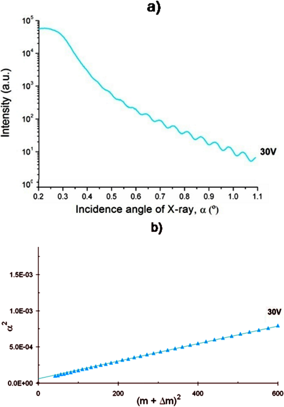
(a) Sample of an XRR line of a coating; (b) Plot of the relationship used to calculate the thickness of the films using the XRR data (case of an anodic film)
The spacing between oscillations changes from one sample to another, and the film thickness is inversely related to this increase and can be used to determine the thickness using the modified Bragg's Law [28], which relates the film thickness t with specific parameters, as follows:
where λ is the wavelength of the incident X-ray, α is the angle for either the maximum or minimum values of the oscillations (peaks or valleys), m is the order of reflection, Δm denotes assigned values of 0 for the peaks and ½ for the valleys, and αc is the critical angle for the total reflection of the X-rays.
Using Equation 2, the thickness t can be determined by plotting α2 vs. (m+Δm)2. The results are linear relationships, as shown in Figure 1.b, with a negligible scatter of the points. By applying this procedure for all the samples, we obtained the film thicknesses, which are presented in Table 1. The error in thickness is 5%; all the calculations were fitted with a R2 coefficient larger than 0.97.
The XRR curves of the samples 60 V and 40 V+1tt show very shallow oscillations (see Figure 5.b), and for that reason the method described above is not applicable and so a method using Discrete Fourier Transform was used [29]. This method is based in the analysis of the power density of oscillating signals; as such, this could be used to identify the main frequencies. Each frequency is related to a unique layer thickness, and if multilayer or fractions of layers are founded on the sample, the XRR will be a linear combination of the frequency corresponding to each coat. The Fourier Transform method used in the analysis of XRR curves was compared with the results obtained using the modified Bragg's Law to the sample 20 V with a perfect fit.
The relative roughness between the coatings and the substrate was qualitatively evaluated by analysing the different amplitudes of the oscillations of the XRR curves according to Parrat's theory [28,30]. Moreover, the average roughness (Ra) was measured using the Time Group TR200 equipment with a cut-off length of 0.8 mm, a sampling length of 0.8 mm and a number of sampling length of 5.
3. Results and discussion
3.1 Colours of the coatings
The TiO2 coatings obtained by sol-gel and anodic oxidation produced two sets of colourful samples. Some of the samples obtained by different techniques presented similar colours. Since the colour is produced by light interference in the film, it depends upon the film thickness; for that reason, there is a relationship between colour and thickness.
In the case of the sol-gel dip-coating technique, the variables of the coating process which produces films of different colours are the dip-coating velocity, the aging time of the sol, the concentration of the sol and the number of layers of the coating. Increasing the value of any of these variables produced films with colours which were associated with thicker films, as shown in Table 1.
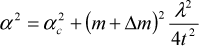
In the sol-gel samples, there was a time evolution of the colour from the beginning of the process, observed during the evaporation of the solvent in drying, which changes from colours associated from thicker to thinner films in a continuous way, according to Table 1. After the heat treatment, there was a high contraction of the film, which led to a different final colour of the coating. The optical micrographs of Figure 2 show the final colour obtained in the monolayer samples after the corresponding heat treatments.

Optical micrographs of the films obtained by the sol-gel technique: (a), (b) and (c): Samples S1, S2 and S3, respectively, obtained with a dilute sol; (d), (e) and (f): Samples S4, S6 and S7 obtained with a concentrated sol
The relationship between colour and thickness can also be seen at the edges of the samples obtained by the sol-gel technique. The edges showed a greater accumulation of liquid during the extraction phase, which caused a greater thickness of the coating in these areas and, therefore, a different colour corresponding to thicknesses greater than those of the central zone of the sample should be obtained.
The optical micrographs of the samples coated by anodic oxidation at different voltages are shown in Figure 3. An homogeneous colour is observed in films obtained between 10 V and 50 V, with a small difference in tone distributed all over the surface in small regions of the size of the grain structure of the substrate, indicating the possible effect of the grain orientation of the substrate phases in the formation of the film [31,32]. The difference in tone was stronger in the films formed at 60 V. One important observation is that there were no changes in colour at the edges of the sample, thus indicating that there was no edge effect on the thickness of the films.
Optical micrographs of the films obtained by anodic oxidation: (a) 10 V; (b) 20 V; (c) 30 V; (d) 40 V; (e) 50 V; (f) 60 V; (g) 20 V+1tt; (h) 40 V+1tt; (i) 60 V+1tt
After the heat treatment in films produced by anodic oxidation at 20 V (20 V+1tt) and 40 V (40 V+1tt), there was an intensification of the blue and green colours, respectively (Figures 3.b, 3.g, 3.d and 3.h). Even after the heat treatment, the coating presents a predominating colour with small patches of another colour. This result indicates that the heat treatment - in the conditions used in this work - slightly modifies the intensity of the colour, maintaining the pattern obtained by anodic oxidation.
The coatings produced by thermal oxidation presented no significant change in colour tonality between the thermal oxide films with a heating ramp (1TT) and those without a heating ramp (1TT-i) (Figures 4.b and 4.a, respectively). However, the 1TT process repeated three times (3TT) led to an increase in the tonality of the golden colour (Figure 4.c). The relationship between colour and thickness obtained with the three techniques is shown in Table 1.

Optical micrographs of oxides formed by thermal oxidation at 500 °C for 1 h: (a) no heating ramp (1TT-i); (b) heated with a ramp and held for 1 h at 500 °C (1TT); (c) same as (b) but repeated three times (3TT)
3.2 Thickness of the coatings
As mentioned in section 2.3, the thickness was measured by using the XRR technique. The XRR curves plotted as intensity versus angle of incidence for the films obtained by the different techniques are shown in Figure 5, and the thickness values are listed in Table 1.

XRR lines of the coatings made by: (a) the sol-gel technique; (b) anodic oxidation without heat treatment; (c) anodic oxidation with heat treatment; (d) thermal oxidation and substrate
Table 1 shows that, with the sol-gel dip-coating technique, the thickness increased when the dip-coating velocity, aging time of the sol, concentration of the sol and number of layers of the coating increased.
In the case of anodic films, the values of thickness versus applied voltage indicated in Table 1 showed a linear relationship, whereby the thickness increased with the voltage at a ratio of 2.4 nm/V.
As the sample which was coated by thermal oxidation (1TT) was 23 nm thick and no increase was observed in the anodic coatings after the heat treatment, it can be concluded that the films obtained by anodic oxidations behave like barriers which prevent thermal oxidations during the heat treatment.
The heat treatment which included a heating ramp led to a 15% increase in thickness with respect to the heat treatment without a ramp. In the case of the 3TT sample, the final thickness was more than three times thinner than the thickness of the 1TT sample. This indicates that the first oxide layers act as partial barriers for oxidation, reducing the diffusion of oxygen through the existing layers. The relationship between colour and thickness obtained with the three techniques is shown in Table 1. It was observed the same relationship between colour and film thickness for all the coating techniques used.
It is necessary to mention that the colour-thickness scale used here is the same as that previously reported for anodic oxidation [5,17]. However, we found no reports of colour vs. thickness for sol-gel films for comparison purposes. In the case of anodic oxidation, the present relationship was confirmed only for the electrolyte that was used, because changing the nature of the electrolyte may produce a different thickness vs. colour relationship [18,19].
In Figure 5.d, the XRR curve corresponding to the substrate is smooth and without any visible oscillation, indicating that the natural oxide thickness is below the sensitivity of the method (which is consistent with the value lower than 10 nm indicated in the literature [1,2]).
3.3 Morphology of the coatings
The shape of the XRR curves (Figure 5) shows that there are differences in the XRR curves of the mono- and multilayer films which could be used to identify each case [30]. The curves of the monolayer films produced by the sol-gel (S2 and S3), the anodic oxidation (10 V to 40 V) and thermal oxidation techniques (1TT and 1TT-i) present uniform and periodic oscillations. In contrast, the curves of the three-layer film produced by the sol-gel technique (S5), anodic oxidation with heat treatment samples (20 V+1tt and 40 V+1tt) and the sample that was thermally treated three times (3TT) are irregular. It is also observed that the monolayer film produced by sol-gel using a highly concentrated sol (S6) also presented an irregular XRR curve, probably due to a density gradient [30] produced during the heat treatment of the 91 nm-thick film.
Moreover, there are differences in the amplitude of the oscillations in the XRR scans of samples made by different techniques. As shown in Figure 5.a, the sol-gel monolayer films presented large oscillations at low values of angles, and as the angle increased the oscillations gradually decrease in amplitude until they disappeared.
In contrast, in the anodic and thermal oxidation monolayer film the oscillations with almost constant amplitude were present throughout the entire scan (Figures 5.b and 5.d, respectively).
According to the theory of reflectometry in thin films developed by Parrat [30], the variation in amplitude of the oscillations in the XRR scans in the monolayer films are related to the coating surface roughness (coating-air roughness) and the roughness of the coating-substrate interface. Since the substrates were prepared in the same way for every coating technique used in this work, they had the same roughness and, therefore, the variations in the amplitude of the oscillations could be associated with the coating surface roughness.
Using Parrat's theory [30], as a consequence both the coating surface roughness and the substrate roughness are similar in the films produced by anodic and thermal oxidation. The roughness of the surface produced by the sol-gel technique is smaller. Therefore, it is possible that the sol-gel technique produced smoother films than the anodic and thermal oxidation techniques, and that the anodic and thermal oxidation techniques produced films that copy the substrate roughness.
Table 2 shows the values of the surface roughness (Ra) of the samples. It can be seen that both the samples obtained by anodic oxidation with and without heat treatment and those that were thermally oxidized gave values of surface roughness Ra similar to those of the substrate. Regarding the samples covered by sol-gel, some gave smaller values of roughness, thus indicating that they were softer.
Roughness (Ra) of the samples

Figure 6 shows the SEM images of the sol-gel monolayer samples. Neither cracks nor pores are observed in the central surface of the samples obtained by the sol-gel (Figures 6.a and 6.b). However, near the edges, the thickness is larger than in the centre of the surface due to the drainage process, and therefore some cracks may be formed near it [14]. Cracks appear in monolayer films because the thickness is greater than the critical value of around 142 nm (Figure 6.c). This value may be achieved on the edges, which explains the cracks observed in it. Three-layer films (S5) were made only with a diluted sol up to a maximum thickness of 75 nm and no cracks on the surfaces were observed.

SEM images of the sol-gel monolayer samples: (a) S4; (b) S6; (c) S7
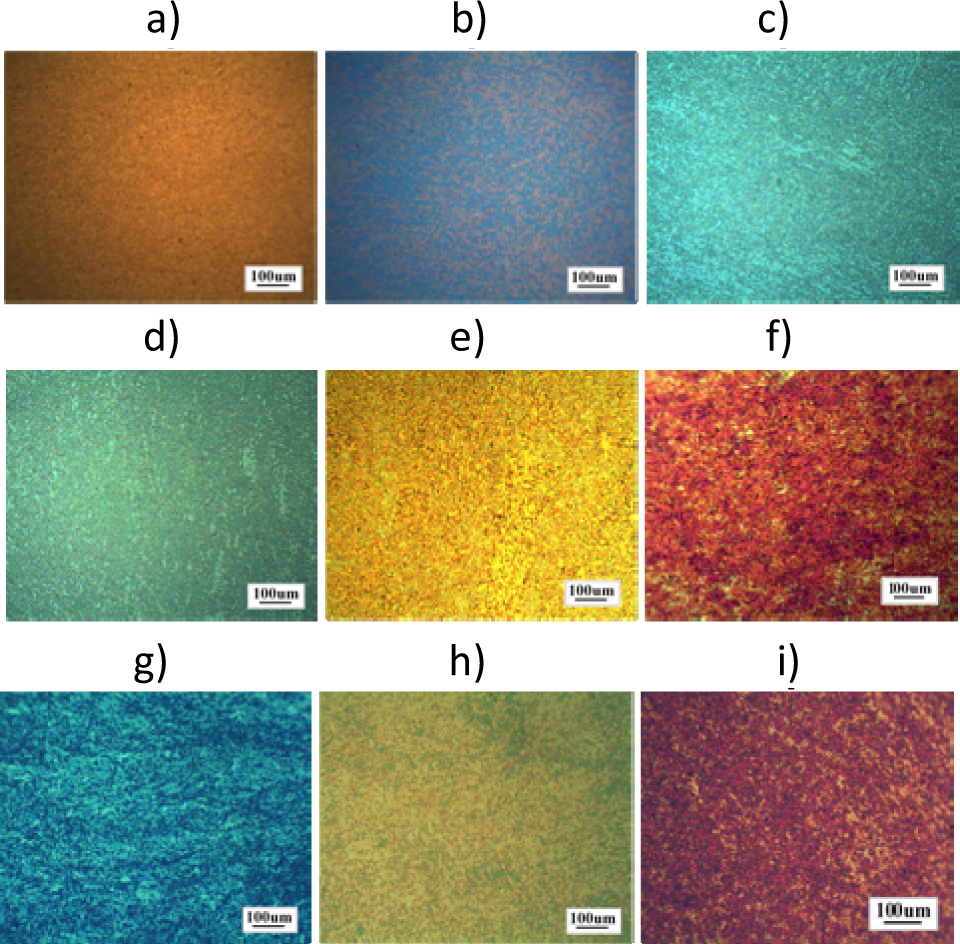
The films produced by anodic oxidation were homogeneous, smooth and compact when the voltage was below 60 V (Figure 7.a). At 60 V and higher voltages, some pores were observed (Figure 7.b); this porous formation is associated with the start of the phenomenon of spark discharge, which derives from an oxidation process called ‘Anodic Spark Deposition’ and which is used to produce porous films with a thickness up to several micrometres [20,21].
The heat treatment applied to the films obtained at 20 V and 40 V did not cause significant changes in the film quality (Figure 4.c).
SEM images of the anodized samples: (a) 40 V; (b) 60 V; (c) 40 V+1tt
3.4 Structure of the coatings
The diffractograms of the films, as well as the diffractogram of the substrate Ti-6Al-4V without a coating, are shown in Figure 8. They are given in normalized intensities for the comparison of the relative amounts of the crystalline phases. All the diffractograms show peaks corresponding to the α and β phases of the biphasic Ti-6Al-4V alloy used as a substrate. The presence of the crystalline phases of TiO2 can be determined from the presence of the main peak of the anatase phase (101) at 2θ 25.29 ° or of the rutile phase (110) at 2θ 27.46 ° [26].

Diffractograms of the coatings obtained by: (a) the solgel technique; (b) anodic oxidation with and without heat treatment; (c) thermal oxidation. Label A indicates the anatase peaks, label R the rutile peaks and label α the alpha-phase peaks of the substrate
Figure 8.a shows the sol-gel film diffraction patterns. In the diffractogram of the monolayer sample S6 (which is 91 nm thick) and in the three-layer sample S5 (which is 75 nm thick) it is possible to identify the anatase and rutile phases. On the other hand, in the S3 sample (which is 54 nm thick) and in the sample S2 (which is 33 nm thick) a small peak corresponding to the rutile phase structure was observed.
Figure 8.b shows the diffraction patterns of the anodic oxidation films, with and without heat treatment. The effect of the heat treatment is clear, since the non-treated films showed no detectable peaks of the anatase or rutile phases; however, after the heat treatment, the coatings show the main peaks of anatase and rutile. It can be seen that the intensity of the main peak of anatase increases with the voltage of the anodized sample because as the voltage increases, so does the thickness of the coating and therefore the anatase mass. The presence of rutile in the samples can be associated with the low thickness of the coatings (up to 144 nm) and the crystallite size of both phases (see below), which would activate the transformation of anatase to rutile at a temperature lower than that of 600 °C proposed in the literature [33]
Figure 8.c shows the diffraction patterns of the thermally oxidized films. In the patterns corresponding to the sample 1TT (20 nm thick) and the sample 1TT-i (23 nm thick) the peaks of the anatase and rutile phases were not observed. However, in the patterns corresponding to the sample 3TT (36 nm thick) the rutile peak is evident.
The crystalline phases began to be identified at a minimum thickness of 33 nm. The absence of crystalline peaks in coatings thinner than 33 nm could be explained by the actual absence of crystalline material or else a reduced amount of anatase, which was below the detection limit for the method.
The application of Scherrer's Formula (1) proved that the coatings obtained by anodic oxidation with heat treatment have an average anatase crystallite size of 20 nm (min. 4.5 nm and max. 32 nm), while in the coatings obtained by sol-gel, the anatase crystallites were of an average value of 15 nm (14 nm min. and max. 16 nm).
Regarding the size of the rutile crystallites, the mean values were 4 nm to 5 nm for the anodic oxidation and sol-gel techniques, and in both cases - respectively - with min. 1 nm and max. 8 nm.
While a direct correlation between the parameters analysed in each process and the size of the crystallites of anatase and rutile were not found, it is evident that there is a dependence of the process used to manufacture the coatings upon the nanocrystal sizes of each phase.
The crystallite size may be related to the stability of the crystalline structures in the films. According to theoretical and experimental studies, it is known that anatase is a metastable phase, whose thermodynamic stability is dependent on the size of the crystallite, then the anatase is more stable than rutile when its crystallites are smaller than a critical size [34]. The critical anatase crystallites' size for the anatase-to-rutile transition was reported within a range of 11 nm to 45 nm [34]. In this case, the presence of rutile in the samples treated at 500 °C may be related to the formation - on the metal-amorphous oxide interface - of anatase crystallites exceeding that critical size, due to the surface effects of bi-dimensional crystallization which transform to rutile following a nucleation and growth process.
In the diffractograms for all the heat treated samples -irrespective of coating method - a small asymmetrical broadening to the left of the peaks corresponding to the α phase (fcc Ti) of the substrate material was observed. In contrast, in the same peaks in the uncoated substrate and those coated by anodic oxidation, this effect was not observed. This broadening could be due to a concentration gradient probably produced by the diffusion of oxygen below the film during heat treatment, or else to a deformation due to stress at the film-substrate interface [35]. The analysis of the thermodynamic aspect -as well as of the kinetics - of this process is beyond the scope of this report.
4. Conclusions
The analysis of the thickness, morphology and crystalline structures of TiO2 thin films produced by sol-gel dip-coating and anodic oxidation allows for the conclusion that:
There is a constant relationship between colour and thickness, which allows for the estimation of the film thickness by the film colour, independent of the coating method.
The use of XRR determined that in sol-gel samples the thickness increases with an increase in the following parameters: dip-coating speed, number of layers, titanium butoxide/isopropanol ratio and aging time of the dispersions. In anodic samples, a linear relationship was found between the thickness and the applied voltage, which allows for the estimation of thickness with good precision.
With the anodic and thermal oxidation, the film copies the substrate roughness. In some cases, the sol-gel produced films smoother than the substrate.
The crystalline phases in the oxide films were identified by GI-XRD only in films thicker than 33 nm, independently of the coating technique. The monolayer and multilayer coatings showed the presence of a mix of anatase and rutile phases. Applying heat treatment of 500 °C and 1 h, after anodizing, crystalline TiO2 in anatase and rutile phases are produced without an increase in film thickness.
The sol-gel and anodic oxidation techniques give suitable coatings for prosthetic heart valves that are both low-roughness films and ideal crystalline structures. Optimizing the process conditions could give smooth films, thick enough to potentially offer good mechanical and corrosion resistance. Evaluating these properties and carrying out haemocompatibility assays will define which will be the best coating for a prosthetic heart valve.
Footnotes
5. Acknowledgments
We wish to thank the Laboratório Nacional de Luz Síncrotron (LNLS), Campinas, Sao Paulo, Brazil, for the D12A-XRD1 beamline facilities and the Centro Atómico Constituyentes (Comisión Nacional de Energía Atómica), Argentina, for the scanning microscopy facilities.
We also acknowledge the financial support of the Consejo Nacional de Investigaciones Científicas y Técnicas (CONICET) and the Agencia Nacional de Promoción Científica y Tecnológica (ANPCyT) of Argentina.